TMUX136 6-GHz, 2-Channel, 2:1 Switch, With Power-off ...
26
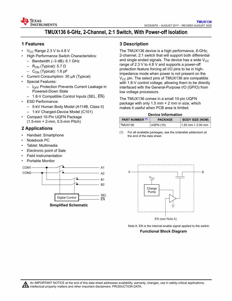
TMUX136 6-GHz, 2-Channel, 2:1 Switch, With Power-off Isolation 1 Features • V CC Range 2.3 V to 4.8 V • High Performance Switch Characteristics: – Bandwidth (–3 dB): 6.1 GHz – R ON (Typical): 5.7 Ω – C ON (Typical): 1.6 pF • Current Consumption: 30 µA (Typical) • Special Features: – I OFF Protection Prevents Current Leakage in Powered-Down State – 1.8-V Compatible Control Inputs (SEL, EN) • ESD Performance: – 5-kV Human Body Model (A114B, Class II) – 1-kV Charged-Device Model (C101) • Compact 10-Pin UQFN Package (1.5-mm × 2-mm, 0.5-mm Pitch) 2 Applications • Handset: Smartphone • Notebook PC • Tablet: Multimedia • Electronic point of Sale • Field instrumentation • Portable Monitor 3 Description The TMUX136 device is a high performance, 6-GHz, 2-channel, 2:1 switch that will support both differential and single ended signals. The device has a wide V CC range of 2.3 V to 4.8 V and supports a power-off protection feature forcing all I/O pins to be in high- impedance mode when power is not present on the V CC pin. The select pins of TMUX136 are compatible with 1.8-V control voltage, allowing them to be directly interfaced with the General-Purpose I/O (GPIO) from low voltage processors. The TMUX136 comes in a small 10-pin UQFN package with only 1.5 mm × 2 mm in size, which makes it useful when PCB area is limited. Device Information PART NUMBER (1) PACKAGE BODY SIZE (NOM) TMUX136 UQFN (10) 1.50 mm × 2.00 mm (1) For all available packages, see the orderable addendum at the end of the data sheet. COM2 COM1 A2 A1 B2 B1 SEL EN Digital Control Simplified Schematic Charge Pump Note A: EN is the internal enable signal applied to the switch. A EN (see Note A) B V CC Functional Block Diagram www.ti.com TMUX136 SCDS367D – AUGUST 2017 – REVISED AUGUST 2020 Copyright © 2020 Texas Instruments Incorporated Submit Document Feedback 1 Product Folder Links: TMUX136 TMUX136 SCDS367D – AUGUST 2017 – REVISED AUGUST 2020 An IMPORTANT NOTICE at the end of this data sheet addresses availability, warranty, changes, use in safety-critical applications, intellectual property matters and other important disclaimers. PRODUCTION DATA.
Transcript of TMUX136 6-GHz, 2-Channel, 2:1 Switch, With Power-off ...
TMUX136 6-GHz, 2-Channel, 2:1 Switch, With Power-off Isolation
1 Features• VCC Range 2.3 V to 4.8 V• High Performance Switch Characteristics:
– Bandwidth (–3 dB): 6.1 GHz– RON (Typical): 5.7 Ω– CON (Typical): 1.6 pF
• Current Consumption: 30 µA (Typical)• Special Features:
– IOFF Protection Prevents Current Leakage inPowered-Down State
– 1.8-V Compatible Control Inputs (SEL, EN)• ESD Performance:
– 5-kV Human Body Model (A114B, Class II)– 1-kV Charged-Device Model (C101)
• Compact 10-Pin UQFN Package(1.5-mm × 2-mm, 0.5-mm Pitch)
2 Applications• Handset: Smartphone• Notebook PC• Tablet: Multimedia• Electronic point of Sale• Field instrumentation• Portable Monitor
3 DescriptionThe TMUX136 device is a high performance, 6-GHz,2-channel, 2:1 switch that will support both differentialand single ended signals. The device has a wide VCCrange of 2.3 V to 4.8 V and supports a power-offprotection feature forcing all I/O pins to be in high-impedance mode when power is not present on theVCC pin. The select pins of TMUX136 are compatiblewith 1.8-V control voltage, allowing them to be directlyinterfaced with the General-Purpose I/O (GPIO) fromlow voltage processors.
The TMUX136 comes in a small 10-pin UQFNpackage with only 1.5 mm × 2 mm in size, whichmakes it useful when PCB area is limited.
Device InformationPART NUMBER (1) PACKAGE BODY SIZE (NOM)
TMUX136 UQFN (10) 1.50 mm × 2.00 mm
(1) For all available packages, see the orderable addendum atthe end of the data sheet.
COM2
COM1
A2
A1
B2
B1
SEL
ENDigital Control
Simplified Schematic
ChargePump
Note A: EN is the internal enable signal applied to the switch.
A
EN (see Note A)
B
VCC
Functional Block Diagram
www.ti.comTMUX136
SCDS367D – AUGUST 2017 – REVISED AUGUST 2020
Copyright © 2020 Texas Instruments Incorporated Submit Document Feedback 1
Product Folder Links: TMUX136
TMUX136SCDS367D – AUGUST 2017 – REVISED AUGUST 2020
An IMPORTANT NOTICE at the end of this data sheet addresses availability, warranty, changes, use in safety-critical applications,intellectual property matters and other important disclaimers. PRODUCTION DATA.
Table of Contents1 Features............................................................................12 Applications..................................................................... 13 Description.......................................................................14 Revision History.............................................................. 25 Pin Configuration and Functions...................................3
Pin Functions.................................................................... 36 Specifications.................................................................. 4
6.1 Absolute Maximum Ratings........................................ 46.2 ESD Ratings............................................................... 46.3 Recommended Operating Conditions.........................46.4 Thermal Information....................................................56.5 Electrical Characteristics.............................................56.6 Dynamic Characteristics............................................. 76.7 Timing Requirements..................................................76.8 Typical Characteristics................................................ 8
7 Parameter Measurement Information............................ 98 Detailed Description...................................................... 11
8.1 Overview................................................................... 118.2 Functional Block Diagram......................................... 11
8.3 Feature Description...................................................118.4 Device Functional Modes..........................................11
9 Application and Implementation.................................. 129.1 Application Information............................................. 129.2 Typical Application.................................................... 12
10 Power Supply Recommendations..............................1611 Layout...........................................................................16
11.1 Layout Guidelines................................................... 1611.2 Layout Example...................................................... 17
12 Device and Documentation Support..........................1812.1 Documentation Support.......................................... 1812.2 Receiving Notification of Documentation Updates..1812.3 Support Resources................................................. 1812.4 Trademarks.............................................................1812.5 Electrostatic Discharge Caution..............................1812.6 Glossary..................................................................18
13 Mechanical, Packaging, and OrderableInformation.................................................................... 18
4 Revision HistoryChanges from Revision C (July 2018) to Revision D (August 2020) Page• Added new specification limits to support added temperature range TA = -40°C to +125°C .............................4
Changes from Revision B (November 2017) to Revision C (July 2018) Page• Changed pin 6 To: EN, pin 7 To: COM2, and pin 8 To: COM1 in Figure 11-2 ..................................................17
Changes from Revision A (October 2017) to Revision B (November 2017) Page• Changed Pin 7 From: COM1 To: COM2............................................................................................................. 3• Changed Pin 8 From: COM2 To: COM1............................................................................................................. 3
Changes from Revision * (August 2017) to Revision A (October 2017) Page• Changed the HBM value From: ±3500 To: ±5000 in the ESD Ratings table...................................................... 4
TMUX136SCDS367D – AUGUST 2017 – REVISED AUGUST 2020 www.ti.com
2 Submit Document Feedback Copyright © 2020 Texas Instruments Incorporated
Product Folder Links: TMUX136
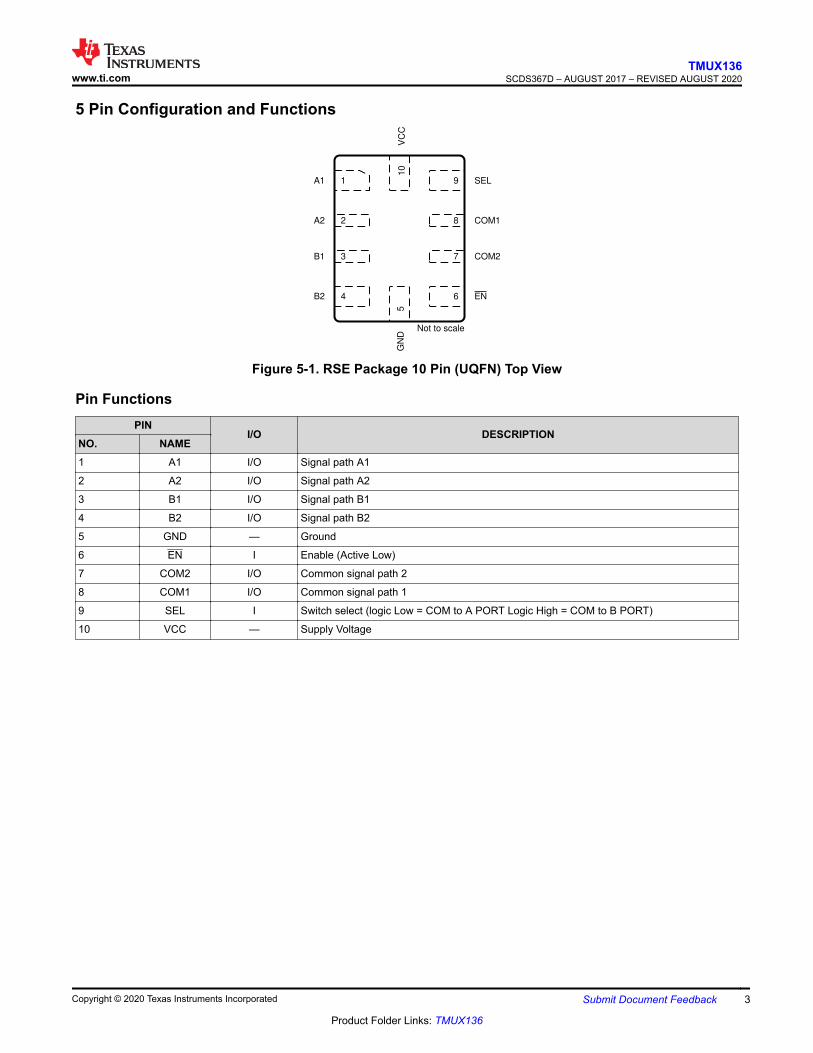
5 Pin Configuration and Functions
1A1
2A2
3B1
4B2
5G
ND
6 EN
7 COM2
8 COM1
9 SEL
10
VC
C
Not to scale
Figure 5-1. RSE Package 10 Pin (UQFN) Top View
Pin FunctionsPIN
I/O DESCRIPTIONNO. NAME1 A1 I/O Signal path A1
2 A2 I/O Signal path A2
3 B1 I/O Signal path B1
4 B2 I/O Signal path B2
5 GND — Ground
6 EN I Enable (Active Low)
7 COM2 I/O Common signal path 2
8 COM1 I/O Common signal path 1
9 SEL I Switch select (logic Low = COM to A PORT Logic High = COM to B PORT)
10 VCC — Supply Voltage
www.ti.comTMUX136
SCDS367D – AUGUST 2017 – REVISED AUGUST 2020
Copyright © 2020 Texas Instruments Incorporated Submit Document Feedback 3
Product Folder Links: TMUX136
6 Specifications6.1 Absolute Maximum Ratingsover operating free-air temperature range (unless otherwise noted)(1) (2)
MIN MAX UNITVCC Supply voltage(3) –0.3 5.5 V
VI/O Input-output DC voltage(3) –0.3 5.5 V
VSEL, V EN Digital input voltage (SEL, EN) –0.3 5.5 V
IK Input-output port diode current VI/O < 0 –50 mA
IIK Digital logic input clamp current(3) VI < 0 –50 mA
ICC Continuous current through VCC 100 mA
IGND Continuous current through GND –100 mA
Tstg Storage temperature –65 150 °C
(1) Stresses beyond those listed under Absolute Maximum Ratings may cause permanent damage to the device. These are stress ratingsonly, which do not imply functional operation of the device at these or any other conditions beyond those indicated underRecommended Operating Conditions. Exposure to absolute-maximum-rated conditions for extended periods may affect devicereliability.
(2) The algebraic convention, whereby the most negative value is a minimum and the most positive value is a maximum.(3) All voltages are with respect to ground, unless otherwise specified.
6.2 ESD RatingsVALUE UNIT
V(ESD)Electrostaticdischarge
Human body model (HBM), per ANSI/ESDA/JEDEC JS-001(1) ±5000V
Charged-device model (CDM), per JEDEC specification JESD22-C101(2) ±1000
(1) JEDEC document JEP155 states that 500-V HBM allows safe manufacturing with a standard ESD control process.(2) JEDEC document JEP157 states that 250-V CDM allows safe manufacturing with a standard ESD control process.
6.3 Recommended Operating ConditionsMIN MAX UNIT
VCC Supply voltage 2.3 4.8 V
VI/O Analog voltage 0 3.6 V
VSEL, V EN Digital input voltage (SEL, EN) 0 VCC V
TRAMP (VCC) Power supply ramp time requirement (VCC) 100 1000 μs/V
II/O Continous current through I/O signal path (COMx, Ax, Bx) TA = –40°C to +85°C ±20 mA
II/O Continous current through I/O signal path (COMx, Ax, Bx) TA = –40°C to +125°C ±10 mA
TA Operating free-air temperature –40 125 °C
TMUX136SCDS367D – AUGUST 2017 – REVISED AUGUST 2020 www.ti.com
4 Submit Document Feedback Copyright © 2020 Texas Instruments Incorporated
Product Folder Links: TMUX136
6.4 Thermal Information
THERMAL METRIC (1)
TMUX136UNITRSE (UQFN)
10 PINSRθJA Junction-to-ambient thermal resistance 191.6 °C/W
RθJC(top) Junction-to-case (top) thermal resistance 94.3 °C/W
RθJB Junction-to-board thermal resistance 117.5 °C/W
ψJT Junction-to-top characterization parameter 7.4 °C/W
ψJB Junction-to-board characterization parameter 117.4 °C/W
(1) For more information about traditional and new thermal metrics, see the Semiconductor and IC Package Thermal Metrics applicationreport.
6.5 Electrical CharacteristicsTA = –40°C to +85°C, Typical values are at VCC = 3.3 V, TA = 25°C, (unless otherwise noted)
PARAMETER TEST CONDITIONS MIN TYP MAX UNITA PORT SWITCH
RON ON-state resistance
VCC = 2.7 V VI/O = 1.65 V, ION = –8 mA 5.7 9
Ω
VCC = 2.3 V VI/O = 1.65 V, ION = –8 mA 5.7 9.5
VCC = 2.7 V VI/O = 1.65 V, ION = –8 mATA = –40°C to +125°C 13
VCC = 2.3 V VI/O = 1.65 V, ION = –8 mATA = –40°C to +125°C 13
ΔRON
ON-state resistancematch between signalpath 1 and 2
VCC = 2.3 V VI/O = 1.65 V, ION = –8 mA 0.1 Ω
RON (FLAT)
ON-state resistanceflatness VCC = 2.3 V VI/O = 1.65 V to 3.45 V, ION = –8 mA 1 Ω
IOZ OFF leakage current VCC = 4.8 V
Switch OFF, VB = 1.65 V to 3.45 V,VCOM = 0 V –2 2
µASwitch OFF, VB = 1.65 V to 3.45 V,VCOM = 0 VTA = –40°C to +125°C
–15 15
IOFFPower-off leakagecurrent VCC = 0 V
Switch ON or OFF, VB = 1.65 V to 3.45 V,VCOM = NC –10 10
µASwitch ON or OFF, VB = 1.65 V to 3.45 V,VCOM = NCTA = –40°C to +125°C
–50 50
ION ON leakage current
VCC = 4.8 V
Switch ON, VB = 1.65 V to 3.45 V,VCOM = NC –2 2
µA
Switch ON, VB = 1.65 V to 3.45 V,VCOM = NCTA = –40°C to +125°C
–15 15
VCC = 2.3 V
Switch ON, VB = 1.65 V to 3.45 V,VCOM = NC –125 125
Switch ON, VB = 1.65 V to 3.45 V,VCOM = NCTA = –40°C to +125°C
–175 175
B PORT SWITCH
RON ON-state resistance VCC = 2.3 VVI/O = 0.4 V, ION = –8 mA 4.6 7.5
Ω VI/O = 0.4 V, ION = –8 mATA = –40°C to +125°C 12
www.ti.comTMUX136
SCDS367D – AUGUST 2017 – REVISED AUGUST 2020
Copyright © 2020 Texas Instruments Incorporated Submit Document Feedback 5
Product Folder Links: TMUX136
TA = –40°C to +85°C, Typical values are at VCC = 3.3 V, TA = 25°C, (unless otherwise noted)PARAMETER TEST CONDITIONS MIN TYP MAX UNIT
ΔRON
ON-state resistancematch between signalpath 1 and 2
VCC = 2.3 V VI/O = 0.4 V, ION = –8 mA 0.1 Ω
RON (FLAT)
ON-state resistanceflatness VCC = 2.3 V VI/O = 0 V to 0.4 V, ION = –8 mA 1 Ω
IOZ OFF leakage current VCC = 4.8 VSwitch OFF, VA = 0 V to 3.6 V, VCOM = 0 V –2 2
µASwitch OFF, VA = 0 V to 3.6 V, VCOM = 0 VTA = –40°C to +125°C –15 15
IOFFPower-off leakagecurrent VCC = 0 V
Switch ON or OFF, VA = 0 V to 3.6 V,VCOM = NC –10 10
µASwitch ON or OFF, VA = 0 V to 3.6 V,VCOM = NCTA = –40°C to +125°C
–50 50
ION ON leakage current
VCC = 4.8 V Switch ON, VA = 0 V to 3.6 V,VD± = NC –2 2
µA
VCC = 4.8 V Switch ON, VA = 0 V to 3.6 V,VD± = NCTA = –40°C to +125°C
–15 15
VCC = 2.3 V Switch ON, VA = 0 V to 3.6 V,VB = NC –125 125
VCC = 2.3 V Switch ON, VA = 0 V to 3.6 V,VB = NCTA = –40°C to +125°C
–175 175
DIGITAL CONTROL INPUTS (SEL, EN)
VIH Input logic high VCC = 2.3 V to 4.8 VTA = –40°C to +125°C 1.3 V
VIL Input logic low VCC = 2.3 V to 4.8 VTA = –40°C to +125°C 0.6 V
IIN Input leakage current VCC = 4.8 V, VI/O = 0 V to 3.6 V, VIN = 0 to 4.8 V –10 10 μA
TMUX136SCDS367D – AUGUST 2017 – REVISED AUGUST 2020 www.ti.com
6 Submit Document Feedback Copyright © 2020 Texas Instruments Incorporated
Product Folder Links: TMUX136
6.6 Dynamic Characteristicsover operating free-air temperature range (unless otherwise noted)
PARAMETER TEST CONDITIONS MIN TYP MAX UNIT
CON
PORT B ON capacitance VCC = 3.3 V, VI/O = 0 or 3.3 V,f = 240 MHz Switch ON 1.6 2 pF
PORT A ON capacitance VCC = 3.3 V, VI/O = 0 or 3.3 V,f = 240 MHz Switch ON 1.4 2 pF
COFF
PORT B OFF capacitance VCC = 3.3 V, VI/O = 0 or 3.3 Vf = 240 MHz Switch OFF 1.4 2 pF
PORT A OFF capacitance VCC = 3.3 V, VI/O = 0 or 3.3 Vf = 240 MHz Switch OFF 1.6 2 pF
CI Digital input capacitance VCC = 3.3 V, VI = 0 or 2 V 2.2 pF
OISO OFF Isolation VCC = 2.3 V to 4.8 V, RL = 50 Ω,f = 240 MHz Switch OFF –34 dB
XTALK Crosstalk VCC = 2.3 V to 4.8 V, RL = 50 Ω,f = 240 MHz Switch ON –37 dB
BW –3-dB bandwidth VCC = 2.3 V to 4.8 V, RL = 50 Ω, Switch ON 6.1 GHz
SUPPLYVCC Power supply voltage 2.3 4.8 V
ICC Positive supply current
VCC = 4.8 V, VIN = VCC or GND, VI/O = 0 V,Switch ON or OFF 30 50
µAVCC = 4.8 V, VIN = VCC or GND, VI/O = 0 V,Switch ON or OFFTA = –40°C to +125°C
70
Icc, HZPower supply current in high-Zmode
VCC = 4.8 V, VIN = VCC or GND, VI/O = 0 V,Switch ON or OFF, OE = H 5 10
µAVCC = 4.8 V, VIN = VCC or GND, VI/O = 0 V,Switch ON or OFF, OE = HTA = –40°C to +125°C
20
6.7 Timing RequirementsMIN NOM MAX UNIT
tpd Propagation delay RL = 50 Ω,CL = 5 pF,VCC = 2.3 V to 4.8 V
100 ps
tswitch Switching time (SEL to output) 600 ns
tZH, ZL Enable time ( EN to output) VI/O = 3.3 V or 0 V 100 µs
tHZ, LZ Disable time ( EN to output) 200 ns
tSK(P) Skew of opposite transitions of same output 20 ps
www.ti.comTMUX136
SCDS367D – AUGUST 2017 – REVISED AUGUST 2020
Copyright © 2020 Texas Instruments Incorporated Submit Document Feedback 7
Product Folder Links: TMUX136
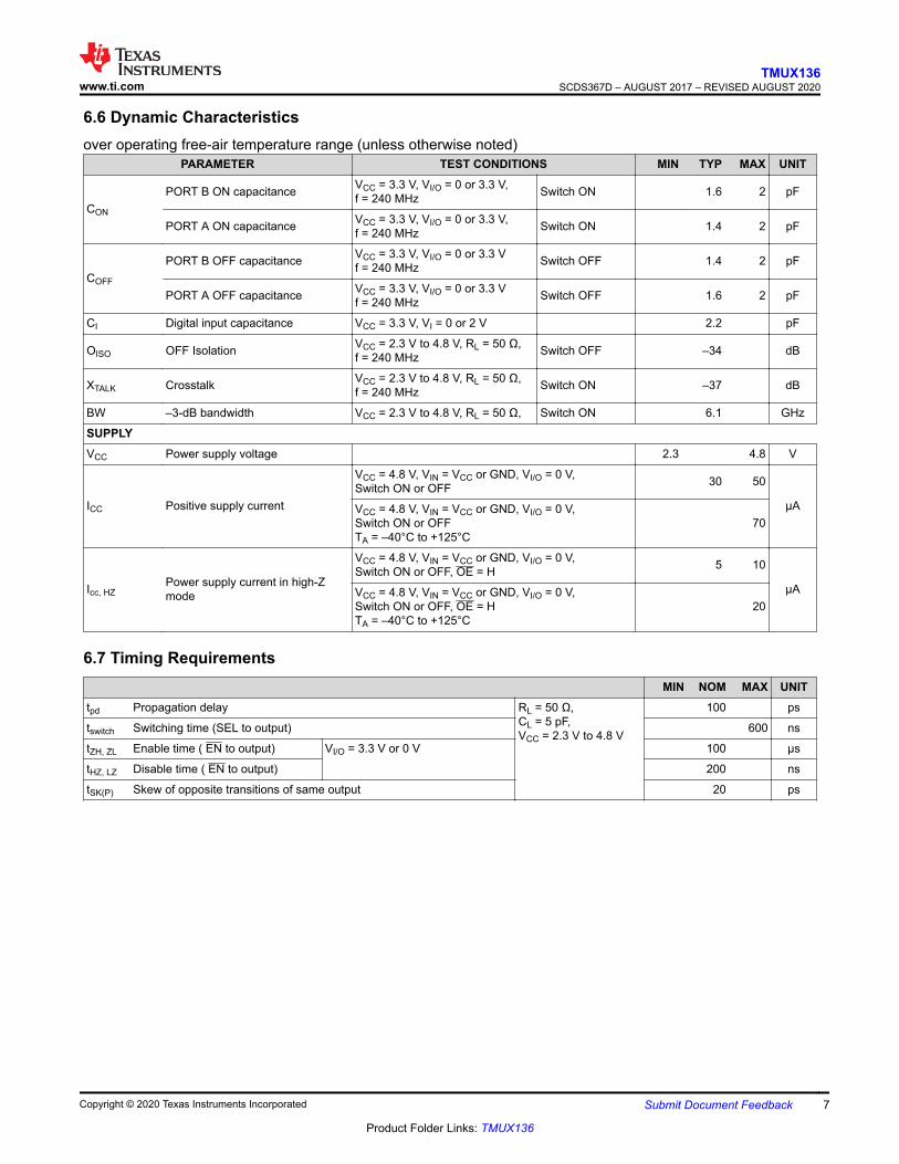
6.8 Typical Characteristics
2.0
2.5
3.0
3.5
4.0
4.5
5.0
5.5
6.0
0.0 0.4 0.8 1.2 1.6 2.0 2.4 2.8 3.2 3.6 4.0
Ro
n (
)
Vin (V) C002
Figure 6-1. ON-Resistance vs VI/OFigure 6-2. Bandwidth
Figure 6-3. Off Isolation Figure 6-4. Cross Talk
TMUX136SCDS367D – AUGUST 2017 – REVISED AUGUST 2020 www.ti.com
8 Submit Document Feedback Copyright © 2020 Texas Instruments Incorporated
Product Folder Links: TMUX136
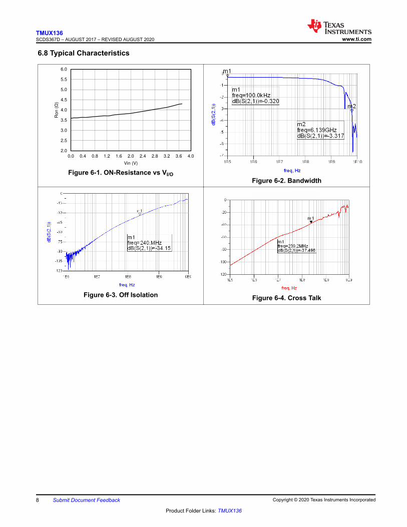
7 Parameter Measurement Information
3 V
SEL RLCL
RLCL
VSEL
VSEL
VA/B
tSWITCH tSWITCH
50 %
50 %
50 %
50 %
1.8 V
3 V
0 V
0 V
COMA
B
Copyright © 2017, Texas Instruments Incorporated
A. All input pulses are suppleid by generators having the following characteristics: PRR ≤ 10 MHz, ZO = 50 Ω , tr < 5 ns, tf < 5 ns.B. CL includes probe and jig capacitance.
Figure 7-1. Timing Diagram
+
+
VSEL
VOUT1
VOUT2
VDD
GND
ION
VON
SEL
Channel ON
RON = (VON – VI/O1) / ION or (VON –VI/O2) / ION
VSEL = H or L
Figure 7-2. ON-State Resistance (RON)
+
+
VSEL
VOUT1
VOUT2
VDD
GND
IOZ
VIN
SEL
+
AChannel OFF
VSEL = H or L
Figure 7-3. OFF Leakage Current (IOZ)
www.ti.comTMUX136
SCDS367D – AUGUST 2017 – REVISED AUGUST 2020
Copyright © 2020 Texas Instruments Incorporated Submit Document Feedback 9
Product Folder Links: TMUX136
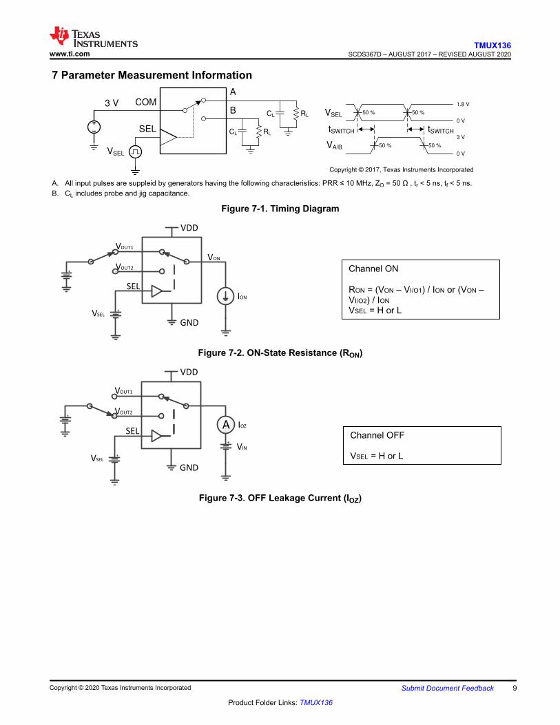
VOUT+
VDD
GND
Network Analyzer
VS
VS
RS
RS
RL
RL
VOUT-
Channel ON
VSEL = H or L
RS=RL=50Ω
Figure 7-4. Bandwidth (BW)
TMUX136SCDS367D – AUGUST 2017 – REVISED AUGUST 2020 www.ti.com
10 Submit Document Feedback Copyright © 2020 Texas Instruments Incorporated
Product Folder Links: TMUX136
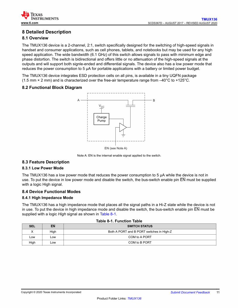
8 Detailed Description8.1 OverviewThe TMUX136 device is a 2-channel, 2:1, switch specifically designed for the switching of high-speed signals inhandset and consumer applications, such as cell phones, tablets, and notebooks but may be used for any highspeed application. The wide bandwidth (6.1 GHz) of this switch allows signals to pass with minimum edge andphase distortion. The switch is bidirectional and offers little or no attenuation of the high-speed signals at theoutputs and will support both signle-ended and differential signals. The device also has a low power mode thatreduces the power consumption to 5 μA for portable applications with a battery or limited power budget.
The TMUX136 device integrates ESD protection cells on all pins, is available in a tiny UQFN package(1.5 mm × 2 mm) and is characterized over the free-air temperature range from –40°C to +125°C.
8.2 Functional Block Diagram
ChargePump
Note A: EN is the internal enable signal applied to the switch.
A
EN (see Note A)
B
VCC
8.3 Feature Description8.3.1 Low Power Mode
The TMUX136 has a low power mode that reduces the power consumption to 5 μA while the device is not inuse. To put the device in low power mode and disable the switch, the bus-switch enable pin EN must be suppliedwith a logic High signal.
8.4 Device Functional Modes8.4.1 High Impedance Mode
The TMUX136 has a high impedance mode that places all the signal paths in a Hi-Z state while the device is notin use. To put the device in high impedance mode and disable the switch, the bus-switch enable pin EN must besupplied with a logic High signal as shown in Table 8-1.
Table 8-1. Function TableSEL EN SWITCH STATUS
X High Both A PORT and B PORT switches in High-Z
Low Low COM to A PORT
High Low COM to B PORT
www.ti.comTMUX136
SCDS367D – AUGUST 2017 – REVISED AUGUST 2020
Copyright © 2020 Texas Instruments Incorporated Submit Document Feedback 11
Product Folder Links: TMUX136
9 Application and ImplementationNote
Information in the following applications sections is not part of the TI component specification, and TIdoes not warrant its accuracy or completeness. TI’s customers are responsible for determiningsuitability of components for their purposes. Customers should validate and test their designimplementation to confirm system functionality.
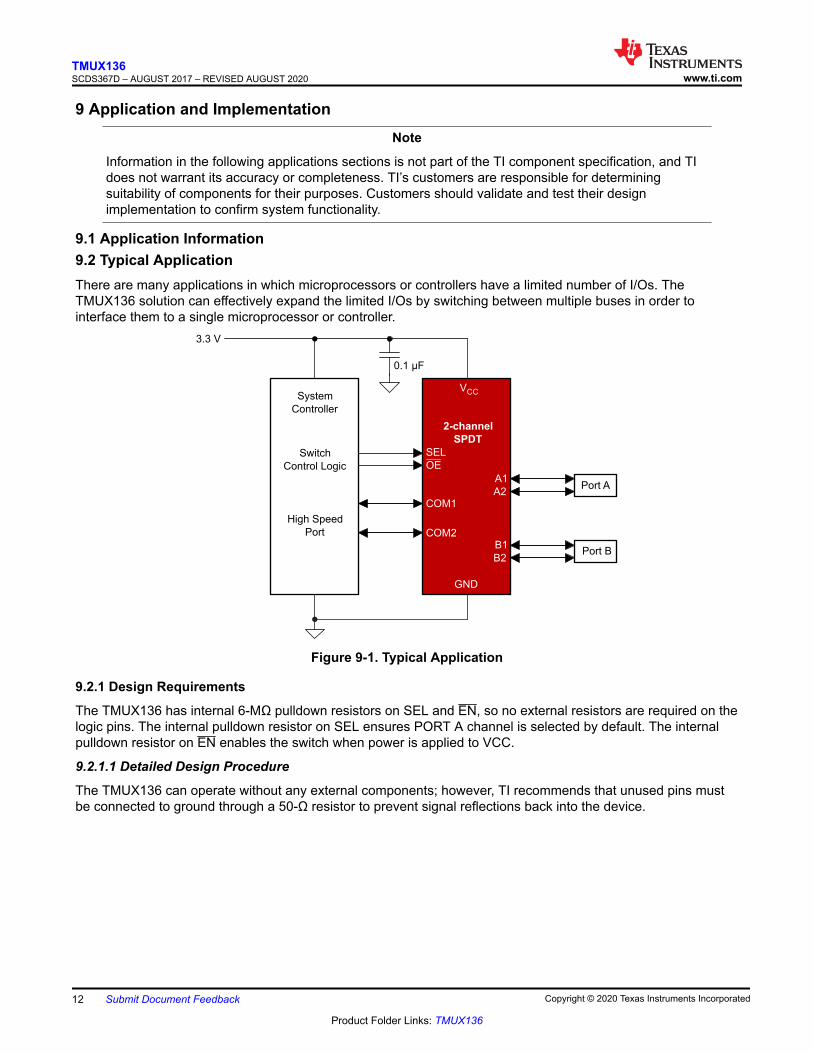
9.1 Application Information9.2 Typical ApplicationThere are many applications in which microprocessors or controllers have a limited number of I/Os. TheTMUX136 solution can effectively expand the limited I/Os by switching between multiple buses in order tointerface them to a single microprocessor or controller.
2-channel
SPDT
VCC
SEL
OE
COM1
COM2
GND
System
Controller
Port A
Port B
0.1 Fμ
3.3 V
High Speed
Port
Switch
Control Logic
B1
B2
A1
A2
Figure 9-1. Typical Application
9.2.1 Design Requirements
The TMUX136 has internal 6-MΩ pulldown resistors on SEL and EN, so no external resistors are required on thelogic pins. The internal pulldown resistor on SEL ensures PORT A channel is selected by default. The internalpulldown resistor on EN enables the switch when power is applied to VCC.
9.2.1.1 Detailed Design Procedure
The TMUX136 can operate without any external components; however, TI recommends that unused pins mustbe connected to ground through a 50-Ω resistor to prevent signal reflections back into the device.
TMUX136SCDS367D – AUGUST 2017 – REVISED AUGUST 2020 www.ti.com
12 Submit Document Feedback Copyright © 2020 Texas Instruments Incorporated
Product Folder Links: TMUX136
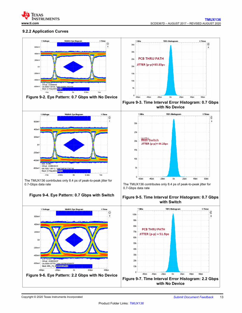
9.2.2 Application Curves
Figure 9-2. Eye Pattern: 0.7 Gbps with No DeviceFigure 9-3. Time Interval Error Histogram: 0.7 Gbps
with No Device
The TMUX136 contributes only 8.4 ps of peak-to-peak jitter for0.7-Gbps data rate
Figure 9-4. Eye Pattern: 0.7 Gbps with Switch
With Switch
The TMUX136 contributes only 8.4 ps of peak-to-peak jitter for0.7-Gbps data rate
Figure 9-5. Time Interval Error Histogram: 0.7 Gbpswith Switch
Figure 9-6. Eye Pattern: 2.2 Gbps with No DeviceFigure 9-7. Time Interval Error Histogram: 2.2 Gbps
with No Device
www.ti.comTMUX136
SCDS367D – AUGUST 2017 – REVISED AUGUST 2020
Copyright © 2020 Texas Instruments Incorporated Submit Document Feedback 13
Product Folder Links: TMUX136
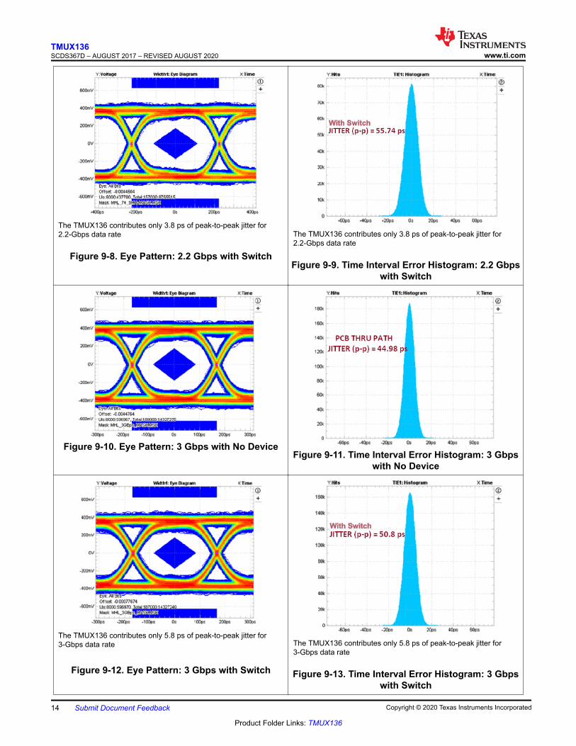
The TMUX136 contributes only 3.8 ps of peak-to-peak jitter for2.2-Gbps data rate
Figure 9-8. Eye Pattern: 2.2 Gbps with Switch
With Switch
The TMUX136 contributes only 3.8 ps of peak-to-peak jitter for2.2-Gbps data rate
Figure 9-9. Time Interval Error Histogram: 2.2 Gbpswith Switch
Figure 9-10. Eye Pattern: 3 Gbps with No DeviceFigure 9-11. Time Interval Error Histogram: 3 Gbps
with No Device
The TMUX136 contributes only 5.8 ps of peak-to-peak jitter for3-Gbps data rate
Figure 9-12. Eye Pattern: 3 Gbps with Switch
With Switch
The TMUX136 contributes only 5.8 ps of peak-to-peak jitter for3-Gbps data rate
Figure 9-13. Time Interval Error Histogram: 3 Gbpswith Switch
TMUX136SCDS367D – AUGUST 2017 – REVISED AUGUST 2020 www.ti.com
14 Submit Document Feedback Copyright © 2020 Texas Instruments Incorporated
Product Folder Links: TMUX136
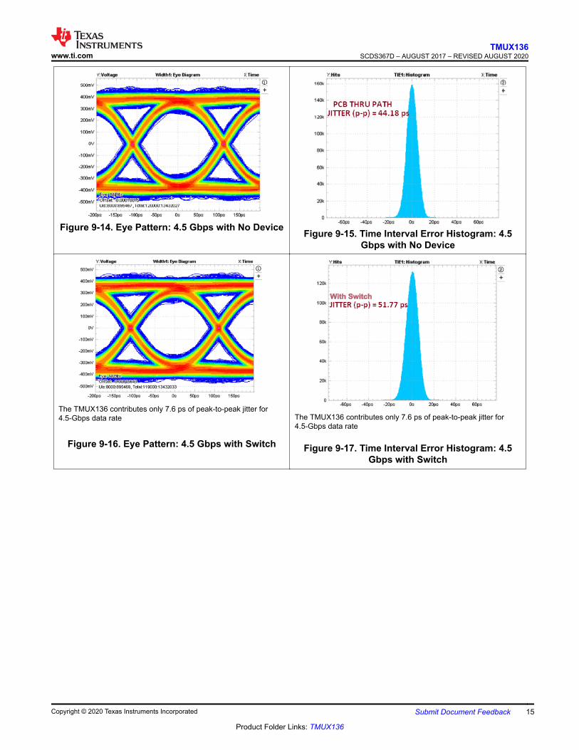
Figure 9-14. Eye Pattern: 4.5 Gbps with No Device Figure 9-15. Time Interval Error Histogram: 4.5Gbps with No Device
The TMUX136 contributes only 7.6 ps of peak-to-peak jitter for4.5-Gbps data rate
Figure 9-16. Eye Pattern: 4.5 Gbps with Switch
With Switch
The TMUX136 contributes only 7.6 ps of peak-to-peak jitter for4.5-Gbps data rate
Figure 9-17. Time Interval Error Histogram: 4.5Gbps with Switch
www.ti.comTMUX136
SCDS367D – AUGUST 2017 – REVISED AUGUST 2020
Copyright © 2020 Texas Instruments Incorporated Submit Document Feedback 15
Product Folder Links: TMUX136
10 Power Supply RecommendationsTI recommends placing a bypass capacitor as close to the supply pin VCC as possible to help smooth out lowerfrequency noise to provide better load regulation across the frequency spectrum.
11 Layout11.1 Layout GuidelinesPlace supply bypass capacitors as close to VCC pin as possible and avoid placing the bypass caps near thehigh speed traces.
The high-speed signalpaths must should be no more than 4 inches long; otherwise, the eye diagramperformance may be degraded.
Route the high-speed signals using a minimum of vias and corners which reduces signal reflections andimpedance changes. When a via must be used, increase the clearance size around it to minimize itscapacitance. Each via introduces discontinuities in the signal’s transmission line and increases the chance ofpicking up interference from the other layers of the board. Be careful when designing test points on twisted pairlines; through-hole pins are not recommended.
When it becomes necessary to turn 90°, use two 45° turns or an arc instead of making a single 90° turn. Thisreduces reflections on the signal traces by minimizing impedance discontinuities.
Do not route high speed signal traces under or near crystals, oscillators, clock signal generators, switchingregulators, mounting holes, magnetic devices or ICs that use or duplicate clock signals.
Avoid stubs on the high-speed signals traces because they cause signal reflections. If a stub is unavoidable,then the stub must be less than 200 mm.
Route all high-speed signal traces over continuous GND planes, with no interruptions.
Avoid crossing over anti-etch, commonly found with plane splits.
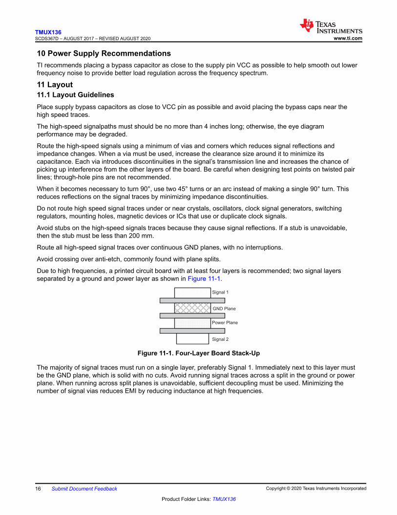
Due to high frequencies, a printed circuit board with at least four layers is recommended; two signal layersseparated by a ground and power layer as shown in Figure 11-1.
Signal 1
GND Plane
Power Plane
Signal 2
Figure 11-1. Four-Layer Board Stack-Up
The majority of signal traces must run on a single layer, preferably Signal 1. Immediately next to this layer mustbe the GND plane, which is solid with no cuts. Avoid running signal traces across a split in the ground or powerplane. When running across split planes is unavoidable, sufficient decoupling must be used. Minimizing thenumber of signal vias reduces EMI by reducing inductance at high frequencies.
TMUX136SCDS367D – AUGUST 2017 – REVISED AUGUST 2020 www.ti.com
16 Submit Document Feedback Copyright © 2020 Texas Instruments Incorporated
Product Folder Links: TMUX136
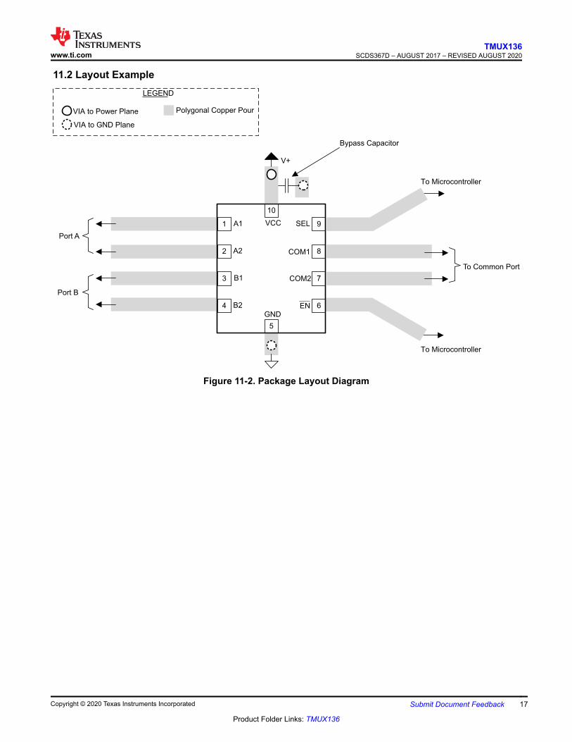
11.2 Layout Example
1
2
3
4
A2
B2
9SEL
COM1
VCC
EN
LEGEND
VIA to Power Plane
VIA to GND Plane
Polygonal Copper Pour
8
7
6
Bypass Capacitor
V+
5
10
B1
GND
A1
To Microcontroller
To Microcontroller
To Common Port
Port A
Port B
COM2
Figure 11-2. Package Layout Diagram
www.ti.comTMUX136
SCDS367D – AUGUST 2017 – REVISED AUGUST 2020
Copyright © 2020 Texas Instruments Incorporated Submit Document Feedback 17
Product Folder Links: TMUX136
12 Device and Documentation Support12.1 Documentation Support12.1.1 Related Documentation
For related documentation see the following:
• High-Speed Layout Guidelines Application Report• High-Speed Interface Layout Guidelines
12.2 Receiving Notification of Documentation UpdatesTo receive notification of documentation updates, navigate to the device product folder on ti.com. Click onSubscribe to updates to register and receive a weekly digest of any product information that has changed. Forchange details, review the revision history included in any revised document.
12.3 Support ResourcesTI E2E™ support forums are an engineer's go-to source for fast, verified answers and design help — straightfrom the experts. Search existing answers or ask your own question to get the quick design help you need.
Linked content is provided "AS IS" by the respective contributors. They do not constitute TI specifications and donot necessarily reflect TI's views; see TI's Terms of Use.
12.4 TrademarksTI E2E™ is a trademark of Texas Instruments.All other trademarks are the property of their respective owners.12.5 Electrostatic Discharge Caution
This integrated circuit can be damaged by ESD. Texas Instruments recommends that all integrated circuits be handledwith appropriate precautions. Failure to observe proper handling and installation procedures can cause damage.ESD damage can range from subtle performance degradation to complete device failure. Precision integrated circuits maybe more susceptible to damage because very small parametric changes could cause the device not to meet its publishedspecifications.
12.6 GlossaryTI Glossary This glossary lists and explains terms, acronyms, and definitions.
13 Mechanical, Packaging, and Orderable InformationThe following pages include mechanical, packaging, and orderable information. This information is the mostcurrent data available for the designated devices. This data is subject to change without notice and revision ofthis document. For browser-based versions of this data sheet, refer to the left-hand navigation.
TMUX136SCDS367D – AUGUST 2017 – REVISED AUGUST 2020 www.ti.com
18 Submit Document Feedback Copyright © 2020 Texas Instruments Incorporated
Product Folder Links: TMUX136
PACKAGE OPTION ADDENDUM
www.ti.com 11-Dec-2021
Addendum-Page 1
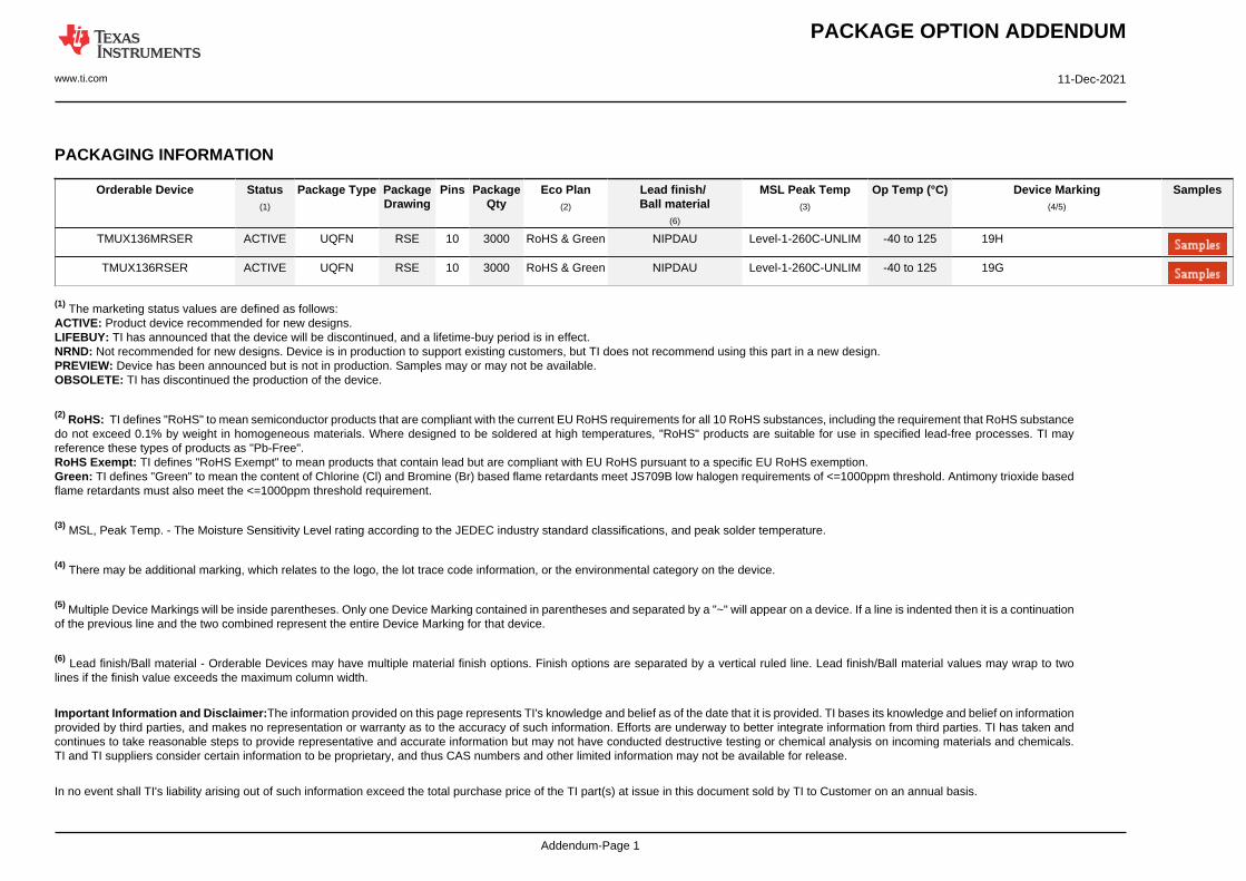
PACKAGING INFORMATION
Orderable Device Status(1)
Package Type PackageDrawing
Pins PackageQty
Eco Plan(2)
Lead finish/Ball material
(6)
MSL Peak Temp(3)
Op Temp (°C) Device Marking(4/5)
Samples
TMUX136MRSER ACTIVE UQFN RSE 10 3000 RoHS & Green NIPDAU Level-1-260C-UNLIM -40 to 125 19H
TMUX136RSER ACTIVE UQFN RSE 10 3000 RoHS & Green NIPDAU Level-1-260C-UNLIM -40 to 125 19G
(1) The marketing status values are defined as follows:ACTIVE: Product device recommended for new designs.LIFEBUY: TI has announced that the device will be discontinued, and a lifetime-buy period is in effect.NRND: Not recommended for new designs. Device is in production to support existing customers, but TI does not recommend using this part in a new design.PREVIEW: Device has been announced but is not in production. Samples may or may not be available.OBSOLETE: TI has discontinued the production of the device.
(2) RoHS: TI defines "RoHS" to mean semiconductor products that are compliant with the current EU RoHS requirements for all 10 RoHS substances, including the requirement that RoHS substancedo not exceed 0.1% by weight in homogeneous materials. Where designed to be soldered at high temperatures, "RoHS" products are suitable for use in specified lead-free processes. TI mayreference these types of products as "Pb-Free".RoHS Exempt: TI defines "RoHS Exempt" to mean products that contain lead but are compliant with EU RoHS pursuant to a specific EU RoHS exemption.Green: TI defines "Green" to mean the content of Chlorine (Cl) and Bromine (Br) based flame retardants meet JS709B low halogen requirements of <=1000ppm threshold. Antimony trioxide basedflame retardants must also meet the <=1000ppm threshold requirement.
(3) MSL, Peak Temp. - The Moisture Sensitivity Level rating according to the JEDEC industry standard classifications, and peak solder temperature.
(4) There may be additional marking, which relates to the logo, the lot trace code information, or the environmental category on the device.
(5) Multiple Device Markings will be inside parentheses. Only one Device Marking contained in parentheses and separated by a "~" will appear on a device. If a line is indented then it is a continuationof the previous line and the two combined represent the entire Device Marking for that device.
(6) Lead finish/Ball material - Orderable Devices may have multiple material finish options. Finish options are separated by a vertical ruled line. Lead finish/Ball material values may wrap to twolines if the finish value exceeds the maximum column width.
Important Information and Disclaimer:The information provided on this page represents TI's knowledge and belief as of the date that it is provided. TI bases its knowledge and belief on informationprovided by third parties, and makes no representation or warranty as to the accuracy of such information. Efforts are underway to better integrate information from third parties. TI has taken andcontinues to take reasonable steps to provide representative and accurate information but may not have conducted destructive testing or chemical analysis on incoming materials and chemicals.TI and TI suppliers consider certain information to be proprietary, and thus CAS numbers and other limited information may not be available for release.
In no event shall TI's liability arising out of such information exceed the total purchase price of the TI part(s) at issue in this document sold by TI to Customer on an annual basis.
PACKAGE OPTION ADDENDUM
www.ti.com 11-Dec-2021
Addendum-Page 2
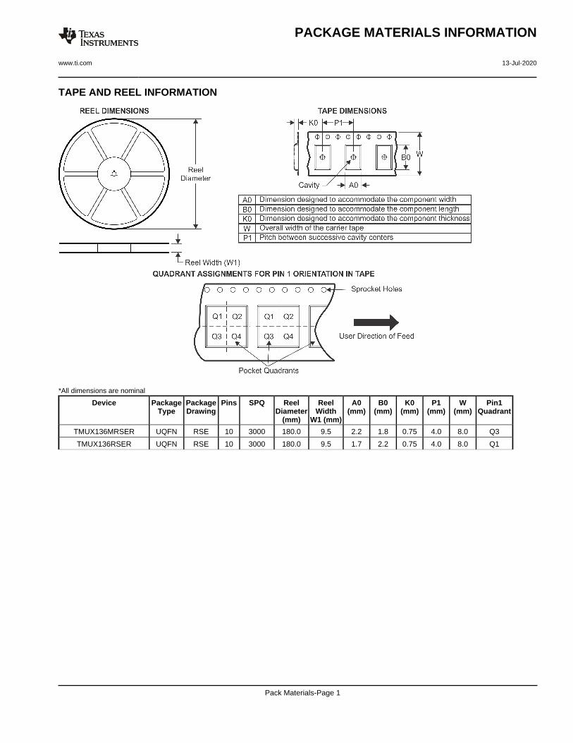
TAPE AND REEL INFORMATION
*All dimensions are nominal
Device PackageType
PackageDrawing
Pins SPQ ReelDiameter
(mm)
ReelWidth
W1 (mm)
A0(mm)
B0(mm)
K0(mm)
P1(mm)
W(mm)
Pin1Quadrant
TMUX136MRSER UQFN RSE 10 3000 180.0 9.5 2.2 1.8 0.75 4.0 8.0 Q3
TMUX136RSER UQFN RSE 10 3000 180.0 9.5 1.7 2.2 0.75 4.0 8.0 Q1
PACKAGE MATERIALS INFORMATION
www.ti.com 13-Jul-2020
Pack Materials-Page 1
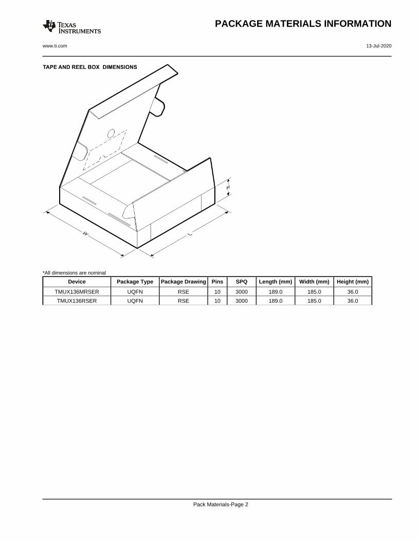
*All dimensions are nominal
Device Package Type Package Drawing Pins SPQ Length (mm) Width (mm) Height (mm)
TMUX136MRSER UQFN RSE 10 3000 189.0 185.0 36.0
TMUX136RSER UQFN RSE 10 3000 189.0 185.0 36.0
PACKAGE MATERIALS INFORMATION
www.ti.com 13-Jul-2020
Pack Materials-Page 2
www.ti.com
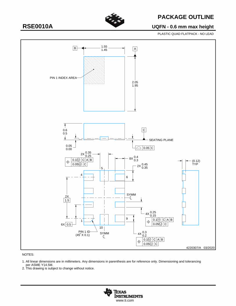
PACKAGE OUTLINE
C0.60.5
0.050.00
2X1.5
6X 0.5
8X 0.40.3
4X 0.30.2
2X 0.450.35
4X 0.250.15
2X 0.350.25
B 1.551.45 A
2.051.95
(0.12)TYP
UQFN - 0.6 mm max heightRSE0010APLASTIC QUAD FLATPACK - NO LEAD
4220307/A 03/2020
PIN 1 INDEX AREA
SEATING PLANE
0.05 C
1
4
5
10
0.1 C A B0.05 C
6
9
SYMM
SYMM
0.1 C A B0.05 C
0.1 C A B0.05 C
PIN 1 ID(45 X 0.1)
NOTES: 1. All linear dimensions are in millimeters. Any dimensions in parenthesis are for reference only. Dimensioning and tolerancing per ASME Y14.5M. 2. This drawing is subject to change without notice.
SCALE 7.000
www.ti.com
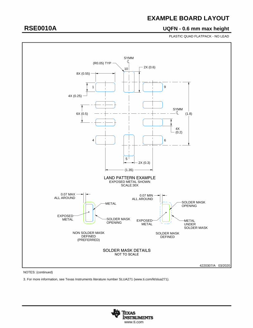
EXAMPLE BOARD LAYOUT
2X (0.6)
2X (0.3)
4X(0.2)
0.07 MINALL AROUND
0.07 MAXALL AROUND
8X (0.55)
4X (0.25)
6X (0.5)
(1.35)
(1.8)
(R0.05) TYP
UQFN - 0.6 mm max heightRSE0010APLASTIC QUAD FLATPACK - NO LEAD
4220307/A 03/2020
SYMM
1
4 6
10
SYMM
LAND PATTERN EXAMPLEEXPOSED METAL SHOWN
SCALE:30X
5
9
NOTES: (continued) 3. For more information, see Texas Instruments literature number SLUA271 (www.ti.com/lit/slua271).
METAL
SOLDER MASKOPENING
SOLDER MASK DETAILSNOT TO SCALE
NON SOLDER MASKDEFINED
(PREFERRED)
EXPOSEDMETAL
SOLDER MASKOPENING
METALUNDERSOLDER MASK
SOLDER MASKDEFINED
EXPOSEDMETAL
www.ti.com
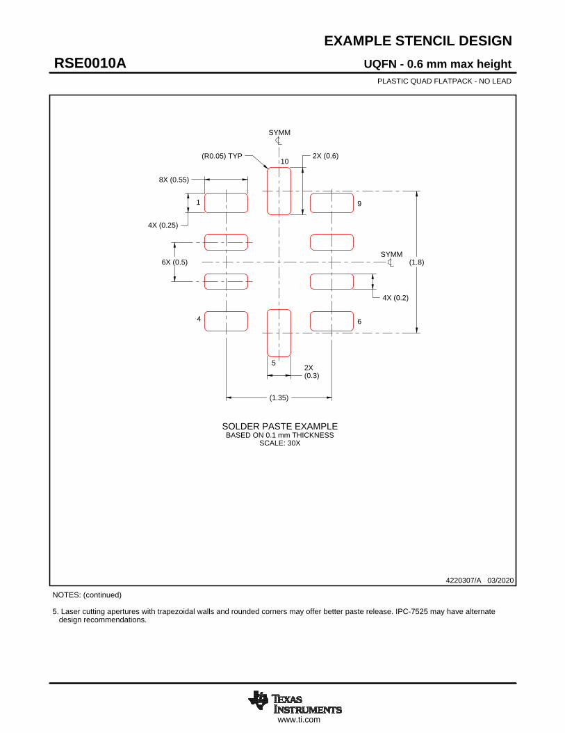
EXAMPLE STENCIL DESIGN
8X (0.55)
4X (0.25)
2X (0.6)
2X(0.3)
(1.35)
(1.8)
4X (0.2)
6X (0.5)
(R0.05) TYP
UQFN - 0.6 mm max heightRSE0010APLASTIC QUAD FLATPACK - NO LEAD
4220307/A 03/2020
NOTES: (continued) 5. Laser cutting apertures with trapezoidal walls and rounded corners may offer better paste release. IPC-7525 may have alternate design recommendations.
SYMM
1
4
5
6
9
10
SYMM
SOLDER PASTE EXAMPLEBASED ON 0.1 mm THICKNESS
SCALE: 30X
IMPORTANT NOTICE AND DISCLAIMERTI PROVIDES TECHNICAL AND RELIABILITY DATA (INCLUDING DATA SHEETS), DESIGN RESOURCES (INCLUDING REFERENCE DESIGNS), APPLICATION OR OTHER DESIGN ADVICE, WEB TOOLS, SAFETY INFORMATION, AND OTHER RESOURCES “AS IS” AND WITH ALL FAULTS, AND DISCLAIMS ALL WARRANTIES, EXPRESS AND IMPLIED, INCLUDING WITHOUT LIMITATION ANY IMPLIED WARRANTIES OF MERCHANTABILITY, FITNESS FOR A PARTICULAR PURPOSE OR NON-INFRINGEMENT OF THIRD PARTY INTELLECTUAL PROPERTY RIGHTS.These resources are intended for skilled developers designing with TI products. You are solely responsible for (1) selecting the appropriate TI products for your application, (2) designing, validating and testing your application, and (3) ensuring your application meets applicable standards, and any other safety, security, regulatory or other requirements.These resources are subject to change without notice. TI grants you permission to use these resources only for development of an application that uses the TI products described in the resource. Other reproduction and display of these resources is prohibited. No license is granted to any other TI intellectual property right or to any third party intellectual property right. TI disclaims responsibility for, and you will fully indemnify TI and its representatives against, any claims, damages, costs, losses, and liabilities arising out of your use of these resources.TI’s products are provided subject to TI’s Terms of Sale or other applicable terms available either on ti.com or provided in conjunction with such TI products. TI’s provision of these resources does not expand or otherwise alter TI’s applicable warranties or warranty disclaimers for TI products.TI objects to and rejects any additional or different terms you may have proposed. IMPORTANT NOTICE
Mailing Address: Texas Instruments, Post Office Box 655303, Dallas, Texas 75265Copyright © 2021, Texas Instruments Incorporated