The problem with linear regulatorstuttle.merc.iastate.edu/ee333/topics/smps/smps_intro.pdfEE 333...
24
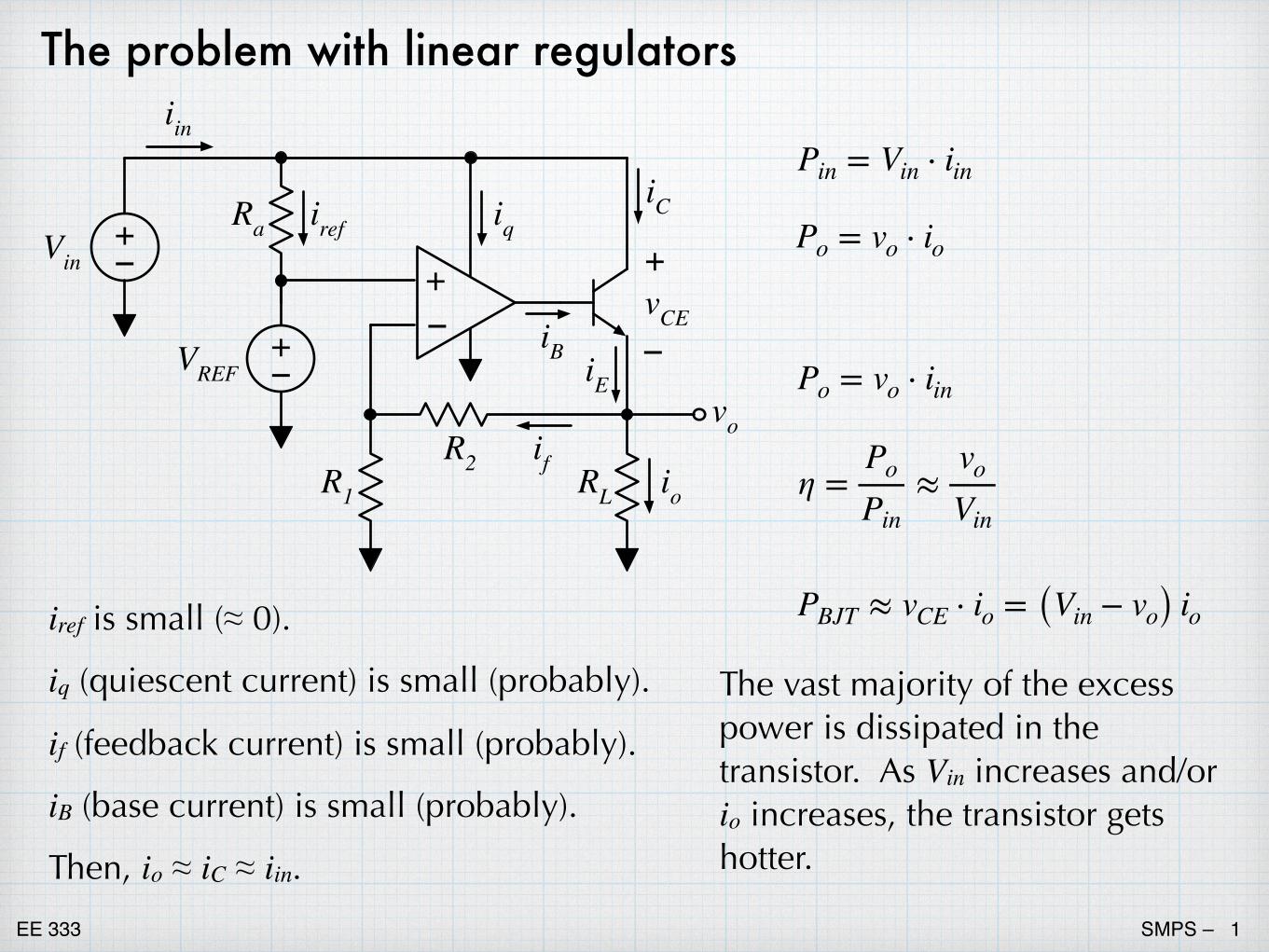
EE 333 SMPS – 1 The problem with linear regulators P in = V in ⋅ i in P o = v o ⋅ i o i ref is small (≈ 0). i q (quiescent current) is small (probably). i f (feedback current) is small (probably). i B (base current) is small (probably). Then, i o ≈ i C ≈ i in . – + + – V REF + – V in R a R 1 R 2 R L i o v o i q i ref i f i in i C – + v CE i B i E P o = v o ⋅ i in η = P o P in ≈ v o V in P BJT ≈ v CE ⋅ i o = ( V in − v o ) i o The vast majority of the excess power is dissipated in the transistor. As V in increases and/or i o increases, the transistor gets hotter.
Transcript of The problem with linear regulatorstuttle.merc.iastate.edu/ee333/topics/smps/smps_intro.pdfEE 333...
EE 333 SMPS – �1
The problem with linear regulators
Pin = Vin ⋅ iin
Po = vo ⋅ io
iref is small (≈ 0).
iq (quiescent current) is small (probably).
if (feedback current) is small (probably).
iB (base current) is small (probably).
Then, io ≈ iC ≈ iin.
–+
+–VREF
+–Vin
Ra
R1R2 RL io
vo
iqiref
if
iin
iC
–
+vCEiB iE Po = vo ⋅ iin
η =Po
Pin≈
vo
Vin
PBJT ≈ vCE ⋅ io = (Vin − vo) io
The vast majority of the excess power is dissipated in the transistor. As Vin increases and/or io increases, the transistor gets hotter.
EE 333 SMPS – �2
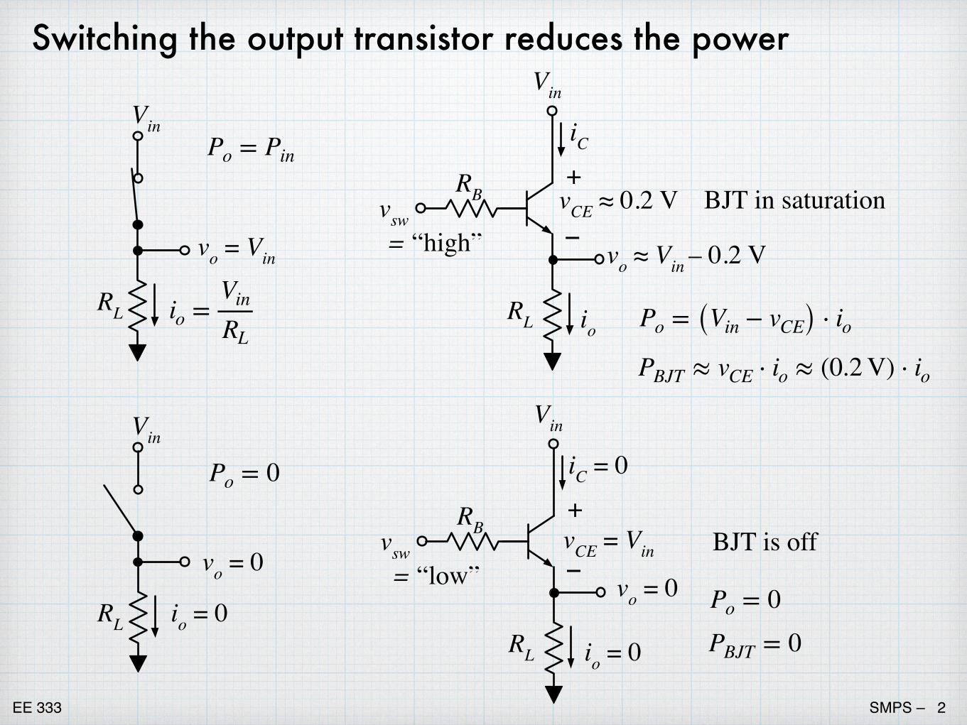
Switching the output transistor reduces the power
Po = (Vin − vCE) ⋅ ioPBJT ≈ vCE ⋅ io ≈ (0.2 V) ⋅ io
BJT in saturation
Vin
vsw
RB
RL
–
+vCE ≈ 0.2 V
iC
vo ≈ Vin – 0.2 V
io
= “high”
Vin
vsw
RB
RL
–
+vCE = Vin
iC = 0
vo = 0= “low”
io = 0
BJT is off
Po = 0PBJT = 0
io =Vin
RL
Vin
RL
vo = Vin
Vin
RL
vo = 0
io = 0
Po = Pin
Po = 0
EE 333 SMPS – �3
Same story with NMOS
Vin
RL
vo = Vin
Vin
RL
vo = 0
io = 0
Vin
vsw
RL
–
+vDS
iD
io
= “high”
io = iD ≈Vin
RL + rDS
vDS ≈ rDS ⋅ iD (small!)
vo = Vin − vDS ≈ Vin
NMOS in ohmic.
Po = (Vin − vDS) ⋅ ioPMOS = vDS ⋅ io (small!)
Po = 0
PMOS = 0
NMOS is off.
Vin
vsw
RL
–
+vDS = Vin
iD = 0
vo = 0= “low”
io = 0
io =Vin
RL
Po = Pin
Po = 0
EE 333 SMPS – �4
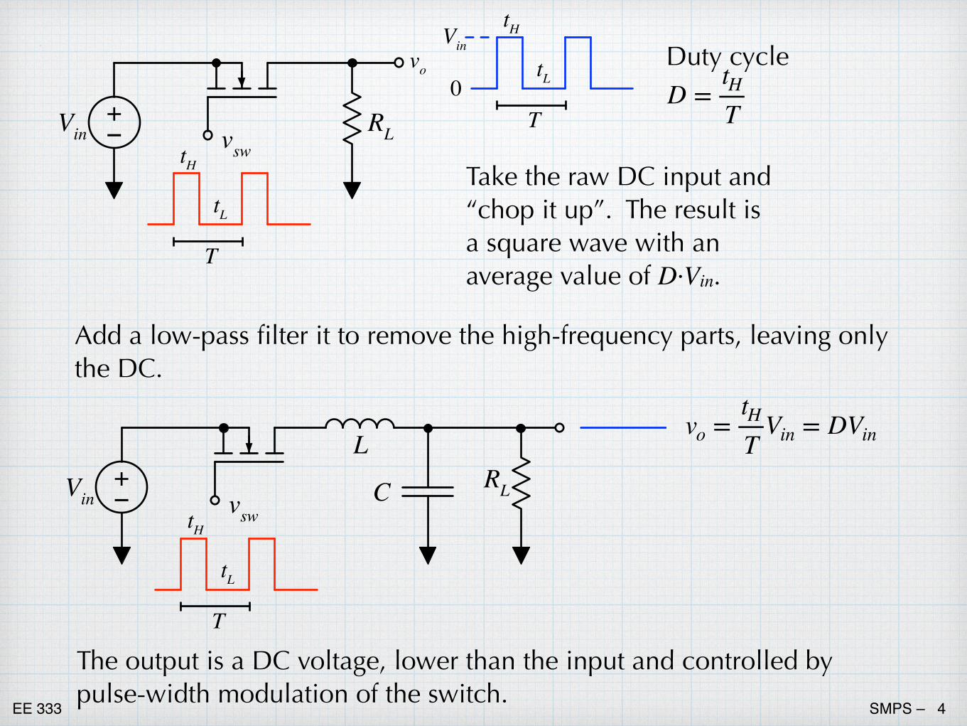
+–Vin vswtH
tL
T
RL
tH
tL
T
Vin
0vo
Take the raw DC input and “chop it up”. The result is a square wave with an average value of D·Vin.
Duty cycleD =
tHT
+–Vin vswtH
tL
T
RLL
C
Add a low-pass filter it to remove the high-frequency parts, leaving only the DC.
vo =tHT
Vin = DVin
The output is a DC voltage, lower than the input and controlled by pulse-width modulation of the switch.
EE 333 SMPS – �5
Switched-mode power supply (SMPS)The previous slide gives a very high-level view of an SMPS. Taking a DC voltage and breaking it up into pieces seems a little strange and possibly counter-productive. But using the transistor in a switched fashion greatly reduces the power dissipated in it. The advantage in power saving greatly outweigh the disadvantage of a more complicated implementation. The obvious advantages:
• Less power wasted. Better for the planet. Better for battery life.
• Since the transistor is dissipating less power, it can be smaller, which means cheaper and more compact.
• Less heat being generated means less heat sinking required, which also means lower cost and lower bulk (size and weight).
There is another extremely important and non-obvious advantage to “switchers”:
• In addition to the “step-down” voltage described on the previous slide, it is also possible to “step-up” (vo > Vin) and “invert” (vo = –Vin), and more. These manner in which these other conversions work are not at all intuitive and require to look at the operation of the circuits some what differently than the simplified description given previously.
EE 333 SMPS – �6
The inductor redeems itselfIn past electronics classes, we were always denigrating the poor inductor. We claimed that we would not allow inductors in our electronics circuits, because they are: bulky (both size and weight), costly (they have lots of atoms), and lossy (due to series resistance). These all go against our electronics “mantra” — faster, smaller, cheaper, and lower power. In order to avoid inductors, we even went to the extreme of making fake inductors using tricky op amp circuits.
In our simplified description of the SMPS from two slides back, the inductor was used as part of a 2nd-order low-pass filter. We might consider trying to use an RC filter (of whatever order) in place of the LC filter. But low-pass RC filters have resistors in series and the capacitor in shunt, meaning that the output current would have to flow through the resistors. An RC circuit may do a good job of filtering, but it would be very lossy! We recall describing an inductor as a fancy short circuit, and an ideal inductor would have no loss. So if we can find a good “real” inductor that has minimal series resistance, the LC filter will be better than an RC filter.
However, viewing the inductor as simply a filter component will not give a complete picture of how switched-mode supplies work. The whole picture is more complicated and subtle. The inductor plays a central in the operation of the circuit. We need to view the inductor an energy storage element and then recall that the are complications when we try to change the inductor current rapidly.
EE 333 SMPS – �7
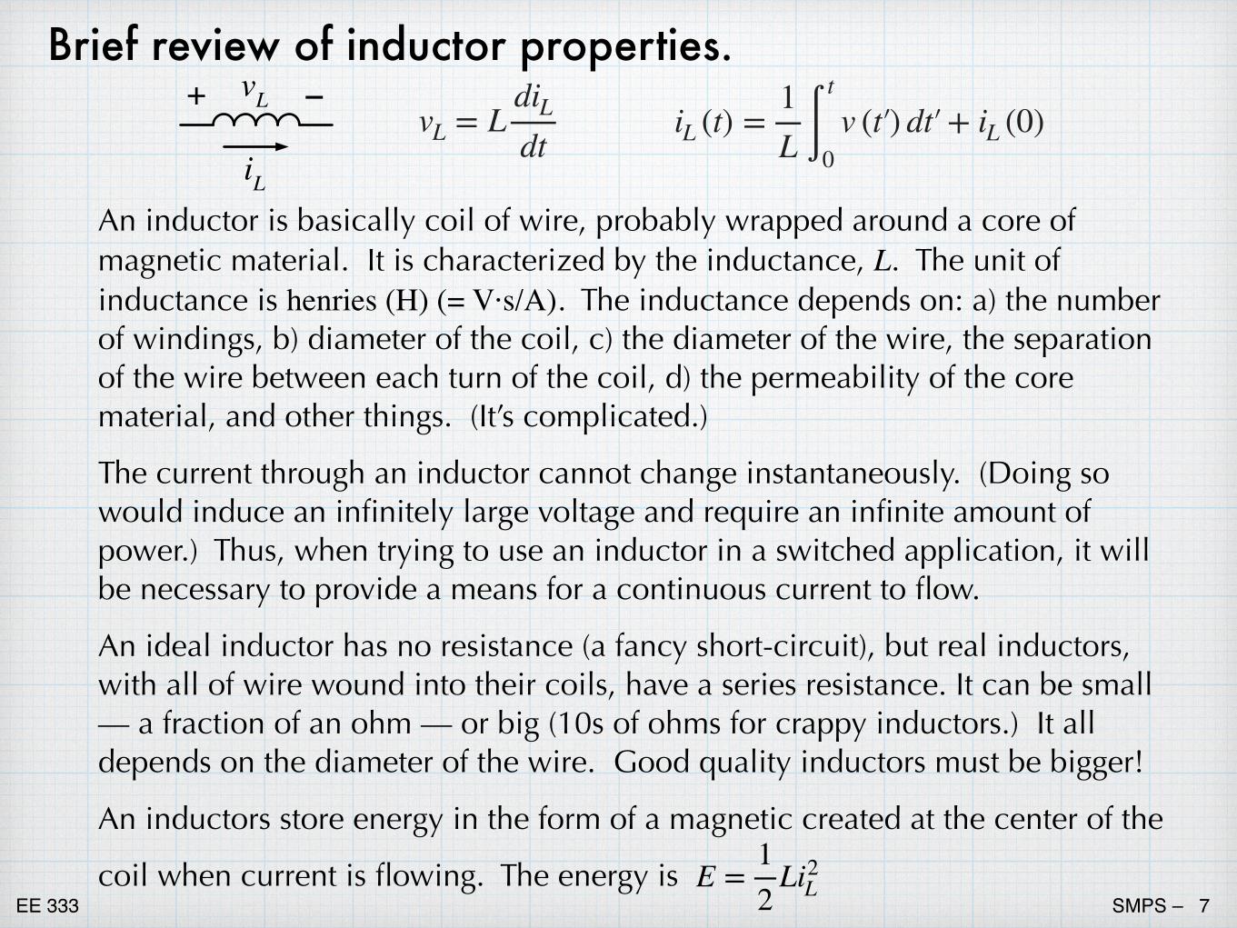
Brief review of inductor properties.vL = L
diLdt
An inductor is basically coil of wire, probably wrapped around a core of magnetic material. It is characterized by the inductance, L. The unit of inductance is henries (H) (= V·s/A). The inductance depends on: a) the number of windings, b) diameter of the coil, c) the diameter of the wire, the separation of the wire between each turn of the coil, d) the permeability of the core material, and other things. (It’s complicated.)
The current through an inductor cannot change instantaneously. (Doing so would induce an infinitely large voltage and require an infinite amount of power.) Thus, when trying to use an inductor in a switched application, it will be necessary to provide a means for a continuous current to flow.
An ideal inductor has no resistance (a fancy short-circuit), but real inductors, with all of wire wound into their coils, have a series resistance. It can be small — a fraction of an ohm — or big (10s of ohms for crappy inductors.) It all depends on the diameter of the wire. Good quality inductors must be bigger!
An inductors store energy in the form of a magnetic created at the center of the
coil when current is flowing. The energy is E =12
Li2L
vL –+
iL
iL (t) =1L ∫
t
0v (t′�) dt′� + iL (0)
EE 333 SMPS – �8
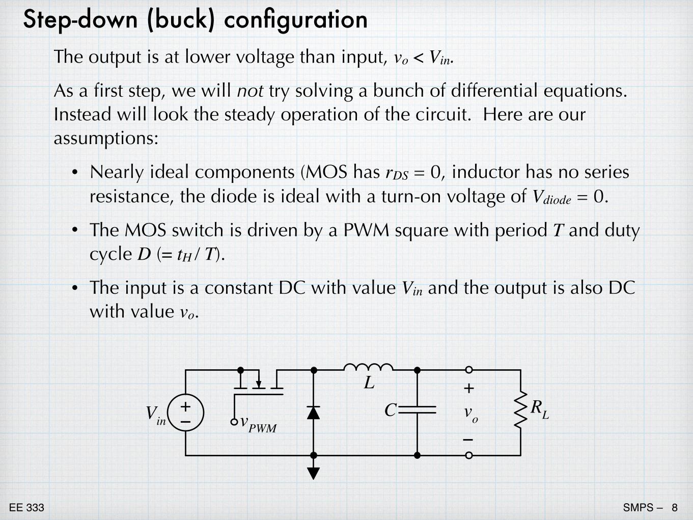
Step-down (buck) configurationThe output is at lower voltage than input, vo < Vin.
As a first step, we will not try solving a bunch of differential equations. Instead will look the steady operation of the circuit. Here are our assumptions:
• Nearly ideal components (MOS has rDS = 0, inductor has no series resistance, the diode is ideal with a turn-on voltage of Vdiode = 0.
• The MOS switch is driven by a PWM square with period T and duty cycle D (= tH / T).
• The input is a constant DC with value Vin and the output is also DC with value vo.
+–Vin vPWM
RLLC vo
–
+
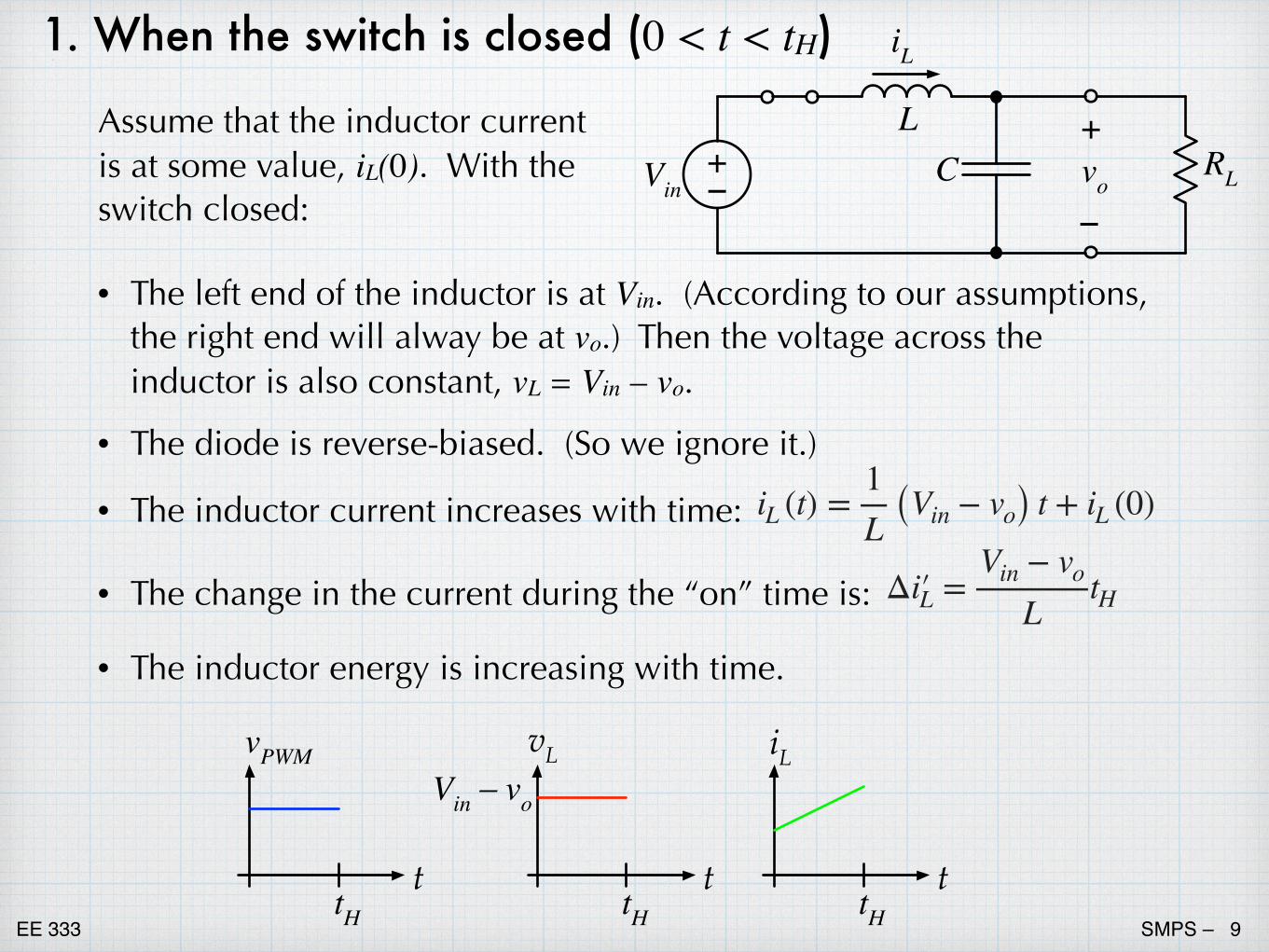
EE 333 SMPS – �9
• The left end of the inductor is at Vin. (According to our assumptions, the right end will alway be at vo.) Then the voltage across the inductor is also constant, vL = Vin – vo.
• The diode is reverse-biased. (So we ignore it.)
• The inductor current increases with time:
• The change in the current during the “on” time is:
• The inductor energy is increasing with time.
1. When the switch is closed (0 < t < tH)
Assume that the inductor current is at some value, iL(0). With the switch closed:
iL (t) =1L (Vin − vo) t + iL (0)
Δi′�L =Vin − vo
LtH
+–Vin RL
LC vo
–
+
iL
vPWM
t
iL
ttH
vLVin – vo
ttH tH
EE 333 SMPS – �10
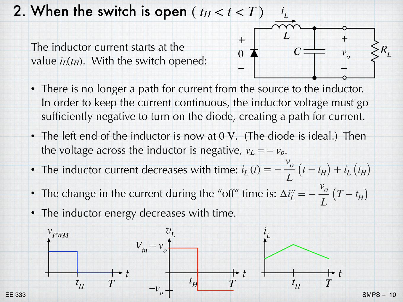
• There is no longer a path for current from the source to the inductor. In order to keep the current continuous, the inductor voltage must go sufficiently negative to turn on the diode, creating a path for current.
• The left end of the inductor is now at 0 V. (The diode is ideal.) Then the voltage across the inductor is negative, vL = – vo.
• The inductor current decreases with time:
• The change in the current during the “off” time is:
• The inductor energy decreases with time.
2. When the switch is open ( tH < t < T )
The inductor current starts at the value iL(tH). With the switch opened:
iL (t) = −vo
L (t − tH) + iL (tH)Δi′�′�L = −
vo
L (T − tH)
vPWM
t
iL
ttH
vLVin – vo
ttH tHT T –voT
RLLC vo
–
+
iL
0–
+
EE 333 SMPS – �11
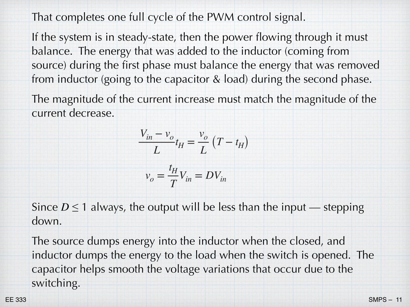
That completes one full cycle of the PWM control signal.
If the system is in steady-state, then the power flowing through it must balance. The energy that was added to the inductor (coming from source) during the first phase must balance the energy that was removed from inductor (going to the capacitor & load) during the second phase.
The magnitude of the current increase must match the magnitude of the current decrease.
Vin − vo
LtH =
vo
L (T − tH)
vo =tHT
Vin = DVin
Since D ≤ 1 always, the output will be less than the input — stepping down.
The source dumps energy into the inductor when the closed, and inductor dumps the energy to the load when the switch is opened. The capacitor helps smooth the voltage variations that occur due to the switching.
EE 333 SMPS – �12
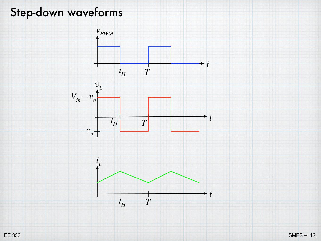
vLVin – vo
ttH T –vo
vPWM
ttH T
iL
ttH T
Step-down waveforms
EE 333 SMPS – �13
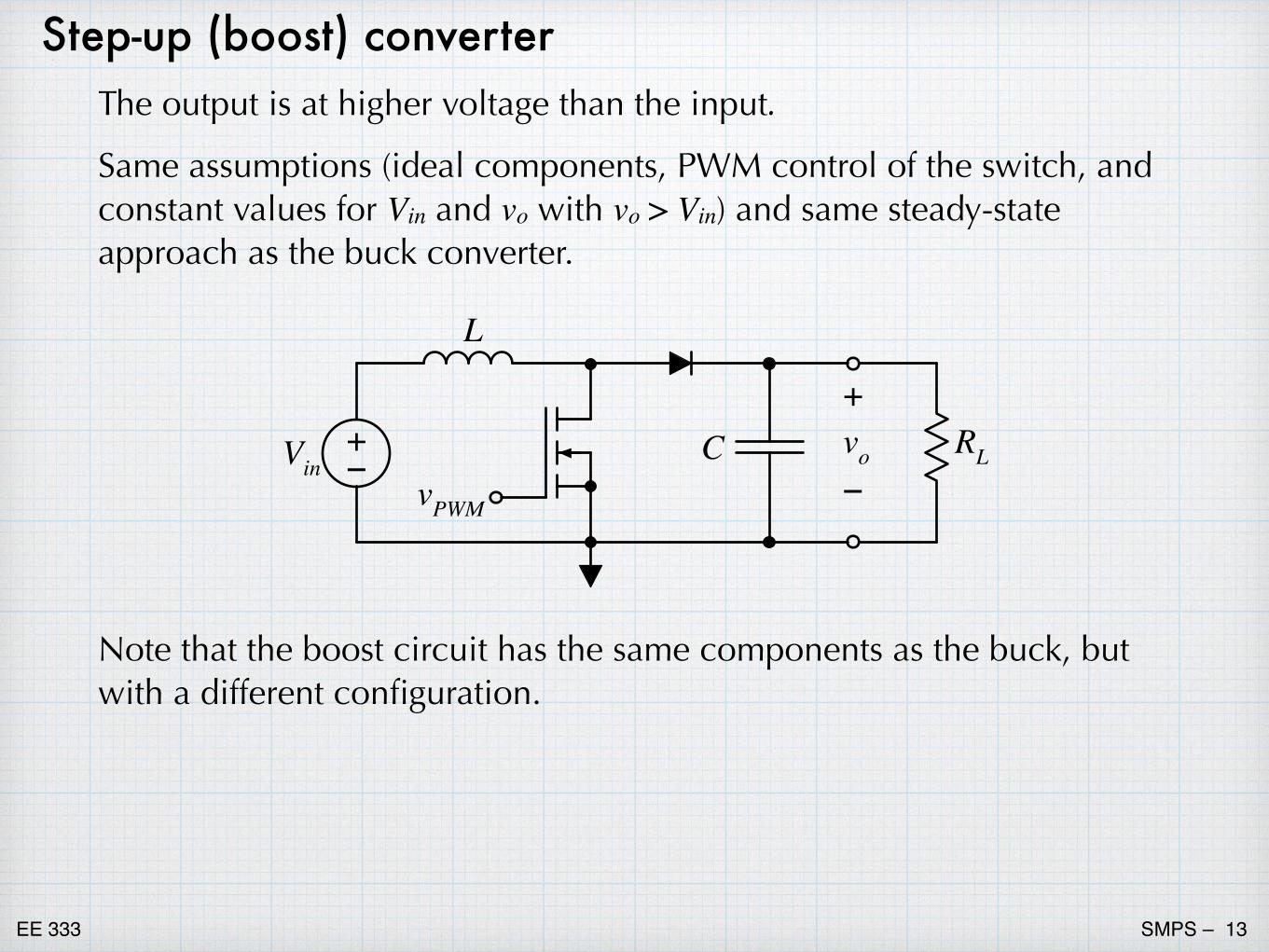
Step-up (boost) converterThe output is at higher voltage than the input.
Same assumptions (ideal components, PWM control of the switch, and constant values for Vin and vo with vo > Vin) and same steady-state approach as the buck converter.
vPWM
RL
L
C vo–
++–Vin
Note that the boost circuit has the same components as the buck, but with a different configuration.
EE 333 SMPS – �14
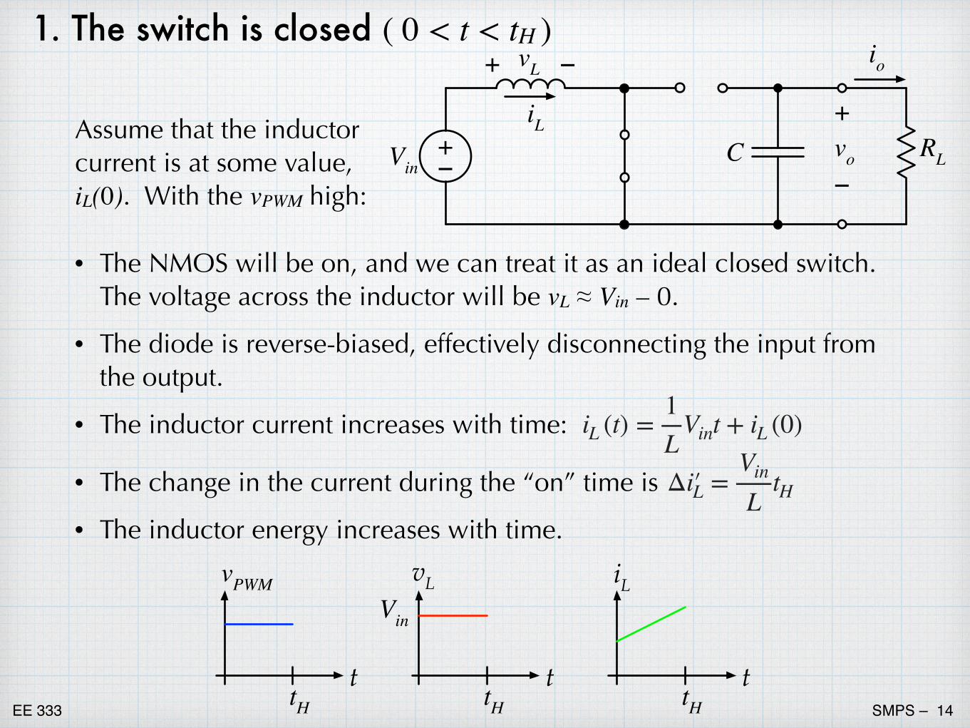
• The NMOS will be on, and we can treat it as an ideal closed switch. The voltage across the inductor will be vL ≈ Vin – 0.
• The diode is reverse-biased, effectively disconnecting the input from the output.
• The inductor current increases with time:
• The change in the current during the “on” time is
• The inductor energy increases with time.
1. The switch is closed ( 0 < t < tH )
Assume that the inductor current is at some value, iL(0). With the vPWM high:
iL (t) =1L
Vint + iL (0)
Δi′�L =Vin
LtH
vPWM
t
iL
ttH
vLVin
ttH tH
RLC vo–
++–Vin
iL
io+ –vL
EE 333 SMPS – �15
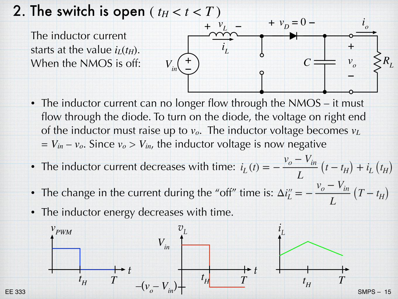
• The inductor current can no longer flow through the NMOS – it must flow through the diode. To turn on the diode, the voltage on right end of the inductor must raise up to vo. The inductor voltage becomes vL = Vin – vo. Since vo > Vin, the inductor voltage is now negative
• The inductor current decreases with time:
• The change in the current during the “off” time is:
• The inductor energy decreases with time.
2. The switch is open ( tH < t < T )
The inductor current starts at the value iL(tH). When the NMOS is off:
iL (t) = −vo − Vin
L (t − tH) + iL (tH)Δi′�′�L = −
vo − Vin
L (T − tH)
RLC vo–
++–Vin
iL
io+ –vL + –vD = 0
iLvLVin
ttH
vPWM
ttH T T –(vo– Vin)
tH T
EE 333 SMPS – �16
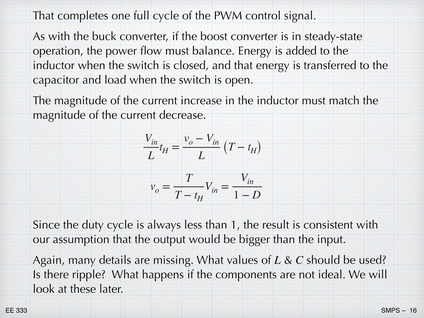
That completes one full cycle of the PWM control signal.
As with the buck converter, if the boost converter is in steady-state operation, the power flow must balance. Energy is added to the inductor when the switch is closed, and that energy is transferred to the capacitor and load when the switch is open.
The magnitude of the current increase in the inductor must match the magnitude of the current decrease.
Vin
LtH =
vo − Vin
L (T − tH)
vo =T
T − tHVin =
Vin
1 − D
Since the duty cycle is always less than 1, the result is consistent with our assumption that the output would be bigger than the input.
Again, many details are missing. What values of L & C should be used? Is there ripple? What happens if the components are not ideal. We will look at these later.
EE 333 SMPS – �17
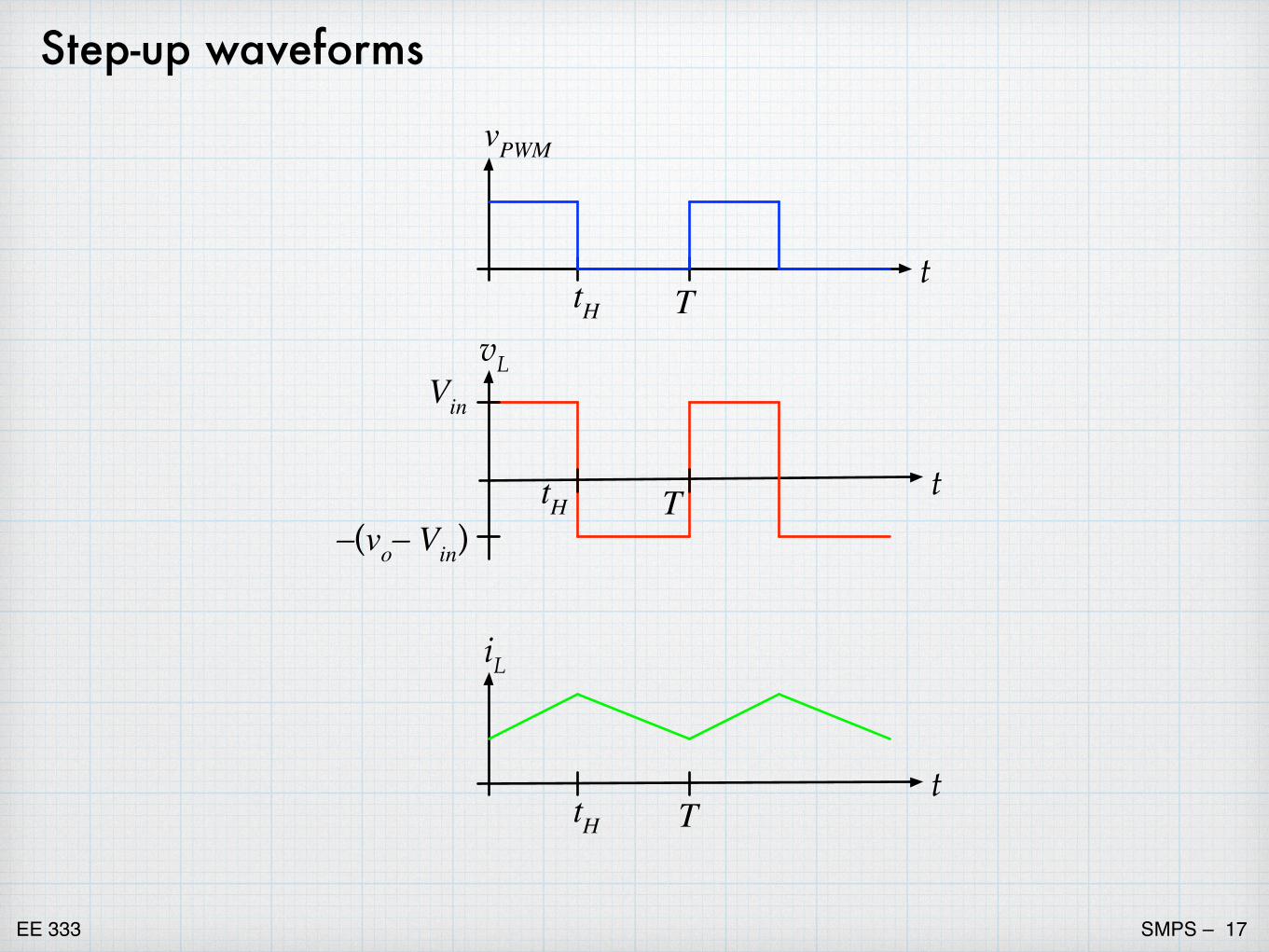
Step-up waveforms
vLVin
ttH T
vPWM
ttH T
iL
ttH T
–(vo– Vin)
EE 333 SMPS – �18
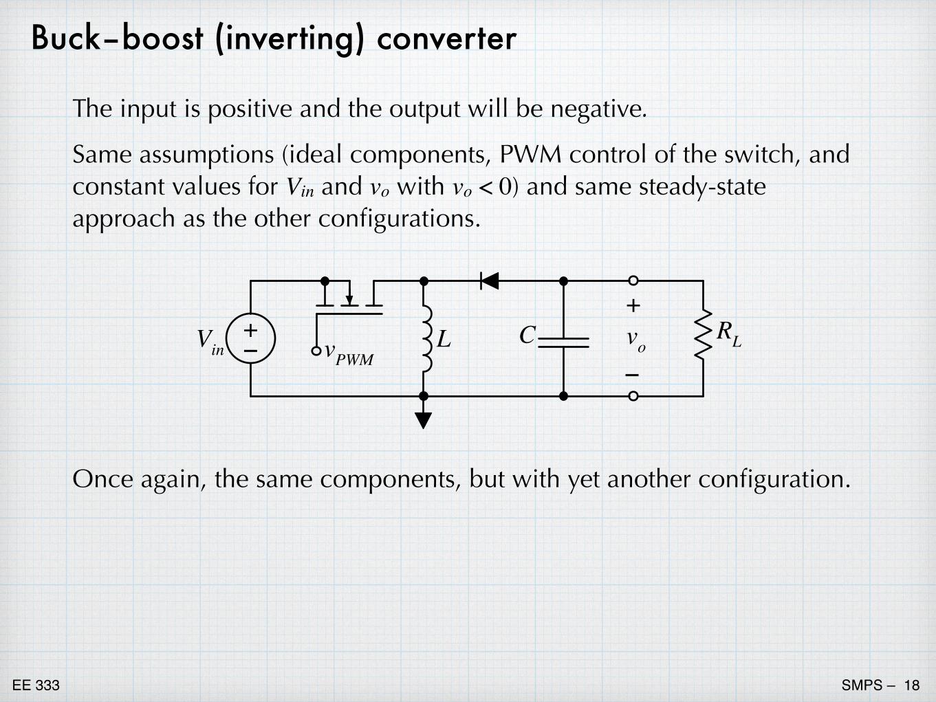
Buck–boost (inverting) converter
The input is positive and the output will be negative.
Same assumptions (ideal components, PWM control of the switch, and constant values for Vin and vo with vo < 0) and same steady-state approach as the other configurations.
Once again, the same components, but with yet another configuration.
+–Vin vPWM
RLL C vo–
+
EE 333 SMPS – �19
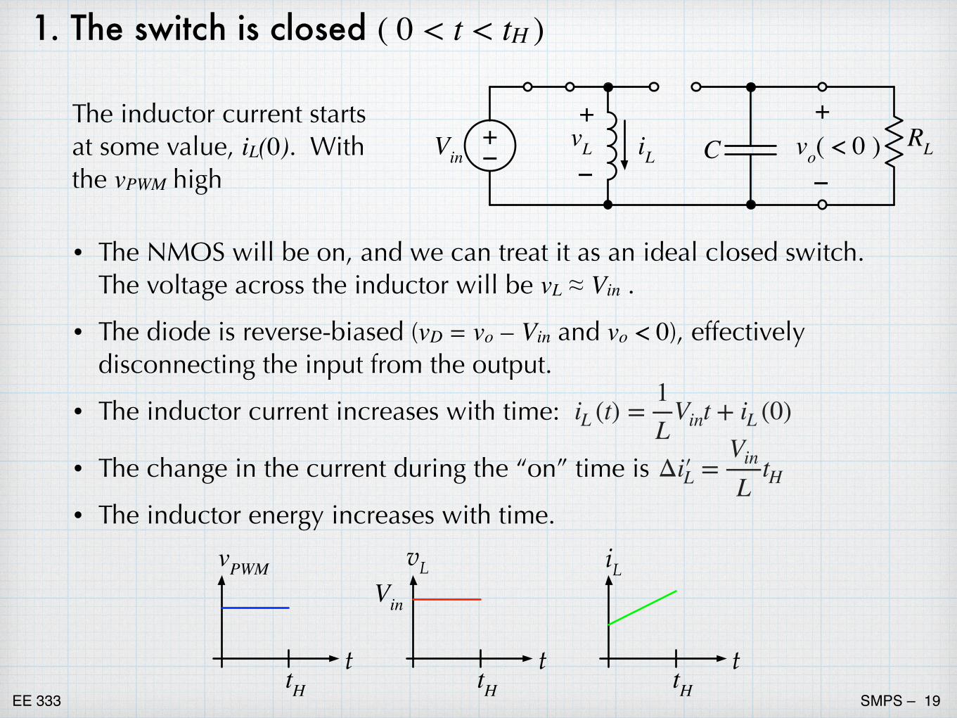
• The NMOS will be on, and we can treat it as an ideal closed switch. The voltage across the inductor will be vL ≈ Vin .
• The diode is reverse-biased (vD = vo – Vin and vo < 0), effectively disconnecting the input from the output.
• The inductor current increases with time:
• The change in the current during the “on” time is
• The inductor energy increases with time.
1. The switch is closed ( 0 < t < tH )
The inductor current starts at some value, iL(0). With the vPWM high
iL (t) =1L
Vint + iL (0)
Δi′�L =Vin
LtH
vPWM
t
iL
ttH
vLVin
ttH tH
+–Vin RLC vo( < 0 )
–
+iL
+
–vL
EE 333 SMPS – �20
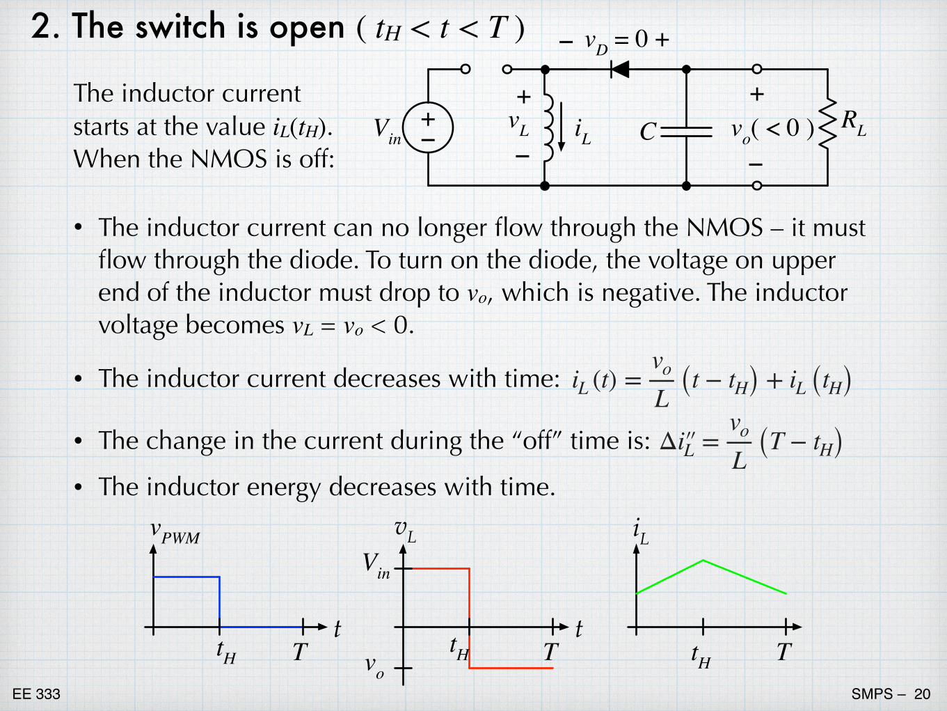
• The inductor current can no longer flow through the NMOS – it must flow through the diode. To turn on the diode, the voltage on upper end of the inductor must drop to vo, which is negative. The inductor voltage becomes vL = vo < 0.
• The inductor current decreases with time:
• The change in the current during the “off” time is:
• The inductor energy decreases with time.
2. The switch is open ( tH < t < T )
The inductor current starts at the value iL(tH). When the NMOS is off:
iL (t) =vo
L (t − tH) + iL (tH)Δi′�′�L =
vo
L (T − tH)
+–Vin
RLC vo( < 0 )–
+iL
+
–vL
– +vD = 0
iLvLVin
ttH
vPWM
ttH T T vo tH T
EE 333 SMPS – �21
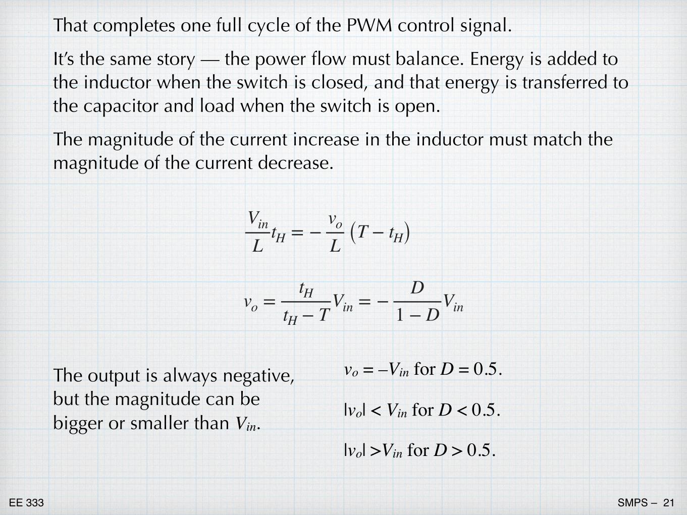
That completes one full cycle of the PWM control signal.
It’s the same story — the power flow must balance. Energy is added to the inductor when the switch is closed, and that energy is transferred to the capacitor and load when the switch is open.
The magnitude of the current increase in the inductor must match the magnitude of the current decrease.
Vin
LtH = −
vo
L (T − tH)
vo =tH
tH − TVin = −
D1 − D
Vin
The output is always negative, but the magnitude can be bigger or smaller than Vin.
vo = –Vin for D = 0.5.
|vo| < Vin for D < 0.5.
|vo| >Vin for D > 0.5.
EE 333 SMPS – �22
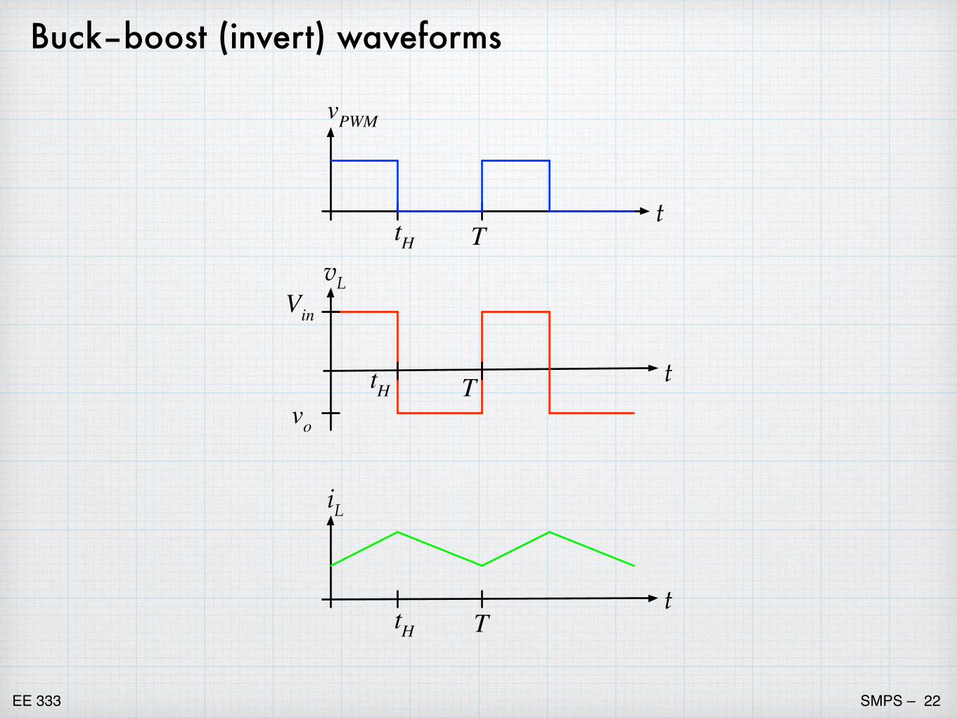
Buck–boost (invert) waveforms
vLVin
ttH T
vPWM
ttH T
iL
ttH T
vo
EE 333 SMPS – �23
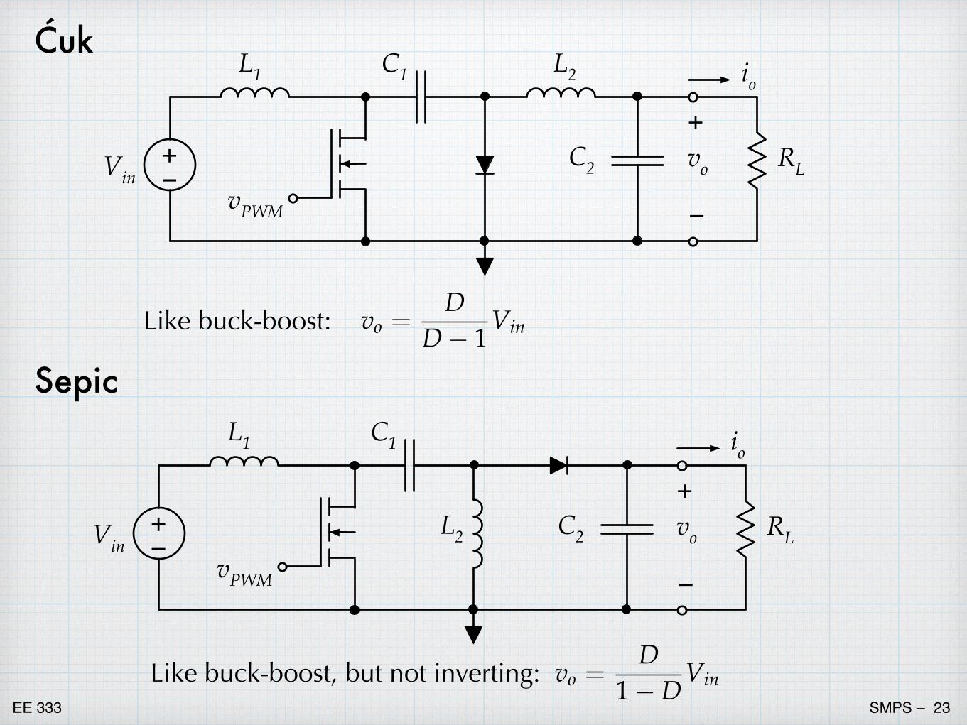
Ćuk
+–Vin
vPWM
io
–
+vo RL
C1L1 L2
C2
vo =D
D � 1VinLike buck-boost:
+–Vin
vPWM
io
–
+vo RL
C1L1
L2 C2
Sepic
vo =D
1� DVinLike buck-boost, but not inverting:
EE 333 SMPS – �24
+–
Vin
vPWM
io
–
+vo RL
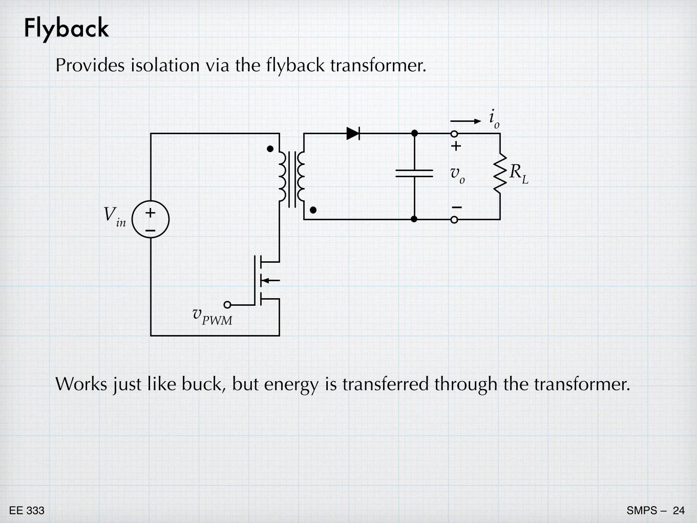
FlybackProvides isolation via the flyback transformer.
Works just like buck, but energy is transferred through the transformer.

![Highly dispersed cobalt Fischer–Tropsch synthesis ... · 322 International Journal of Industrial Chemistry (2019) 10:321–333 1 3 andcobaltcatalysts[10–12].Tobestofourknowledge,gas](https://static.fdocument.org/doc/165x107/5f30fe2e8a907020596e6018/highly-dispersed-cobalt-fischeratropsch-synthesis-322-international-journal.jpg)


![Group14compoundsandcomplexes 333 2_2.pdf · 338 Discussionofdataselection They reported the heat capacity measurements of both Farkas and Eldridge [68FAR/ELD]andSamarukovet al.[74SAM/KOS],whichareingoodagreement](https://static.fdocument.org/doc/165x107/60e63348f56cdf02cb71c8b4/group14compoundsandcomplexes-333-22pdf-338-discussionofdataselection-they-reported.jpg)


![Scanning spectrophotometry and spectrophotometric determination of concentration BCH 333 [practical]](https://static.fdocument.org/doc/165x107/56649dad5503460f94a9c8ed/scanning-spectrophotometry-and-spectrophotometric-determination-of-concentration.jpg)