The Complementarity of Real Space and Reciprocal Spaceneutrons2.ornl.gov/conf/nxs2009/pdf/Lecture 12...
76
The Complementarity of Real Space and Reciprocal Space Lecture at Neutron and X-Ray School J. Murray Gibson June 12, 2009
Transcript of The Complementarity of Real Space and Reciprocal Spaceneutrons2.ornl.gov/conf/nxs2009/pdf/Lecture 12...

The Complementarity of Real Space and Reciprocal Space
Lecture at Neutron and X-Ray SchoolJ. Murray Gibson
June 12, 2009
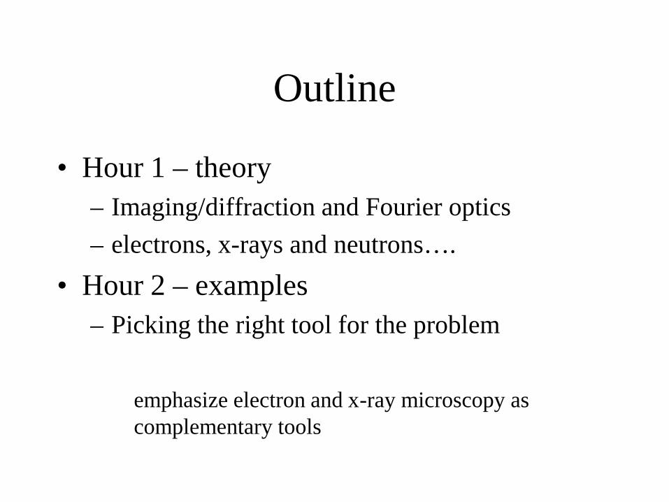
Outline
• Hour 1 – theory– Imaging/diffraction and Fourier optics– electrons, x-rays and neutrons….
• Hour 2 – examples– Picking the right tool for the problem
emphasize electron and x-ray microscopy ascomplementary tools
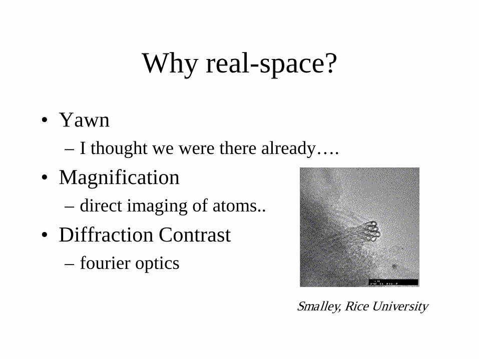
Why real-space?
• Yawn– I thought we were there already….
• Magnification– direct imaging of atoms..
• Diffraction Contrast– fourier optics
Smalley, Rice University
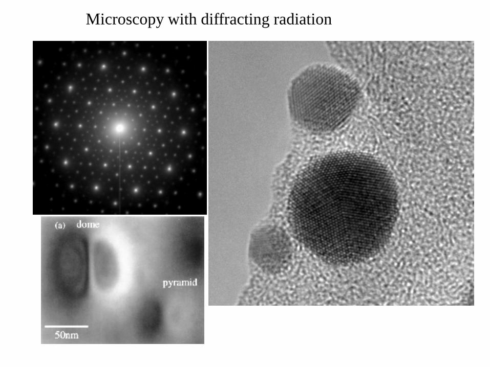
Microscopy with diffracting radiation
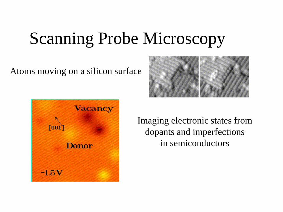
Scanning Probe Microscopy
Imaging electronic states fromdopants and imperfections
in semiconductors
Atoms moving on a silicon surface
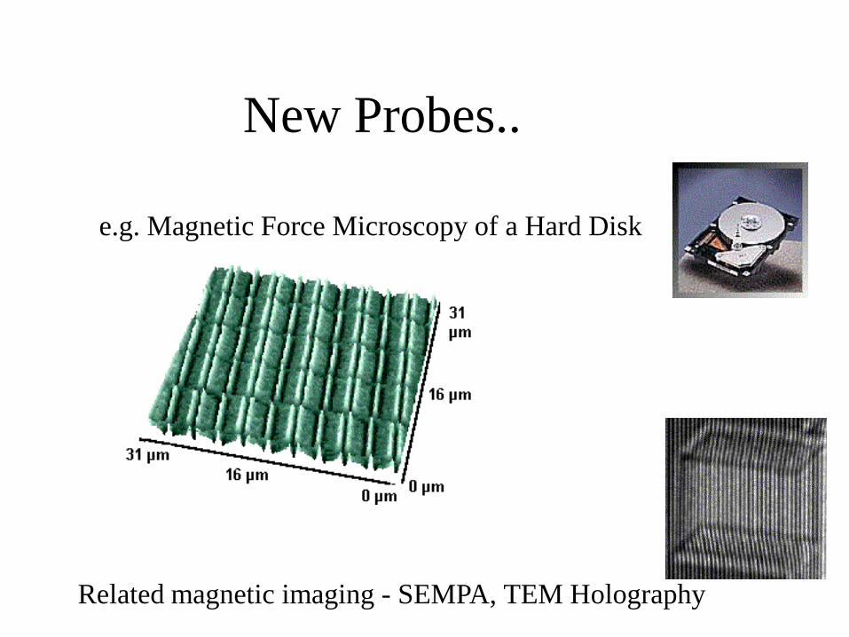
New Probes..
e.g. Magnetic Force Microscopy of a Hard Disk
Related magnetic imaging - SEMPA, TEM Holography
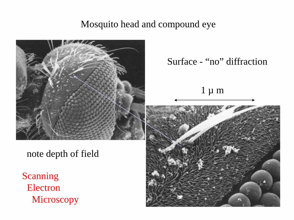
Mosquito head and compound eye
1 µ m
note depth of field
ScanningElectronMicroscopy
Surface - “no” diffraction
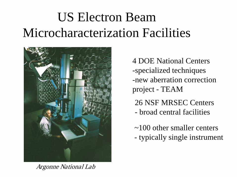
US Electron Beam Microcharacterization Facilities
4 DOE National Centers-specialized techniques-new aberration correctionproject - TEAM
26 NSF MRSEC Centers- broad central facilities
~100 other smaller centers- typically single instrument
Argonne National Lab
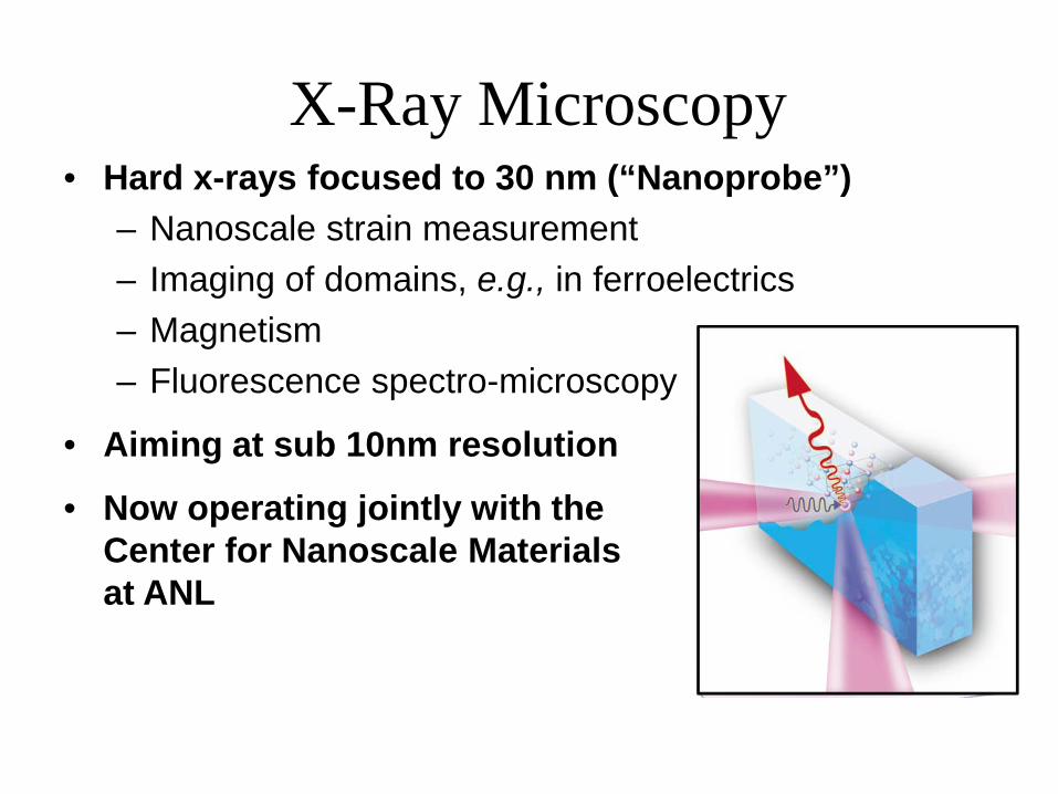
• Hard x-rays focused to 30 nm (“Nanoprobe”)– Nanoscale strain measurement– Imaging of domains, e.g., in ferroelectrics– Magnetism– Fluorescence spectro-microscopy
• Aiming at sub 10nm resolution
• Now operating jointly with the Center for Nanoscale Materialsat ANL
X-Ray Microscopy
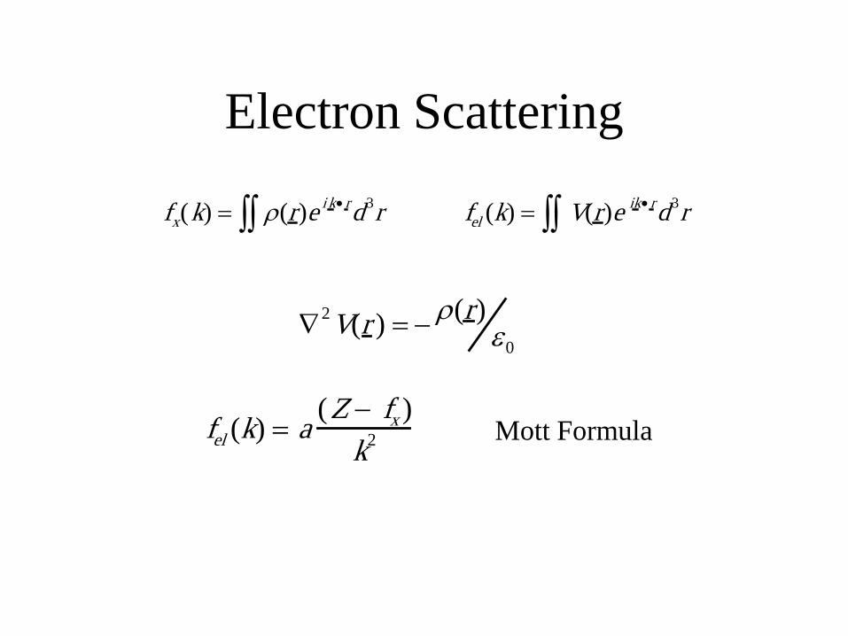
Electron Scattering
fx(k) = ρ(r∫∫ )e i k• rd3r
∇2V(r ) = − ρ(r)ε0
fel (k) = V(r∫∫ )e ik• rd3r
fel (k) = a (Z − fx )k2 Mott Formula
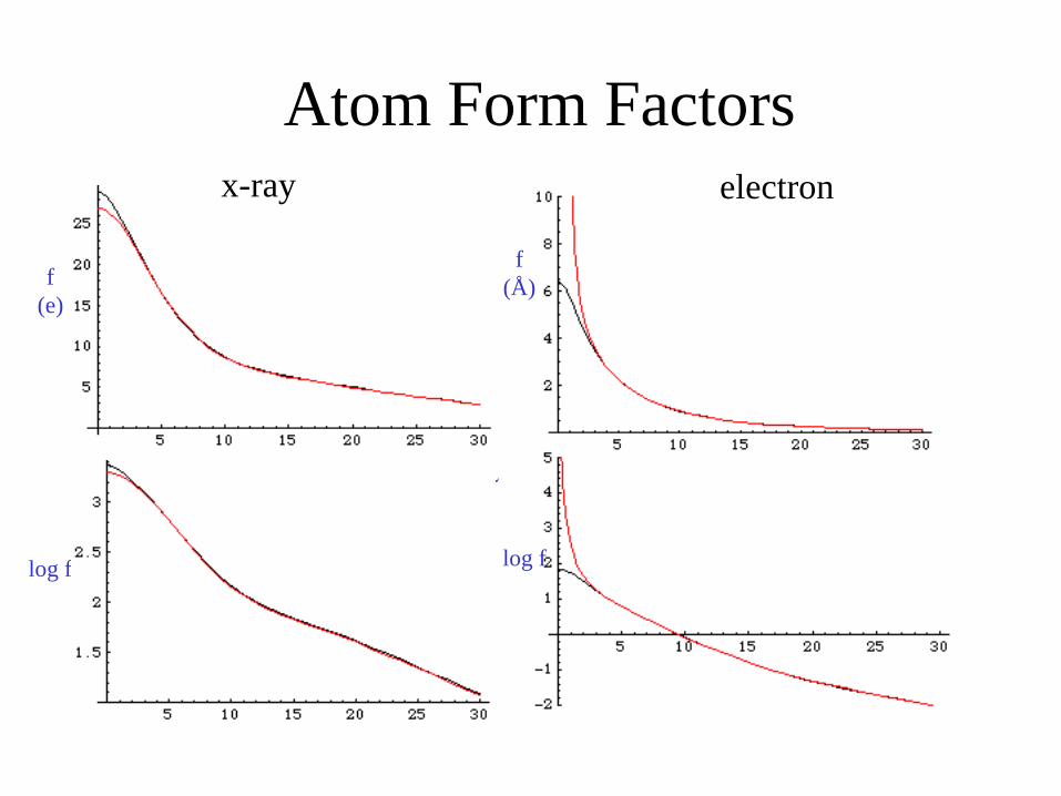
Atom Form Factors
CuCu2+
sinθ /λ
f(e)
log f
f(Å)
log f
electronx-ray
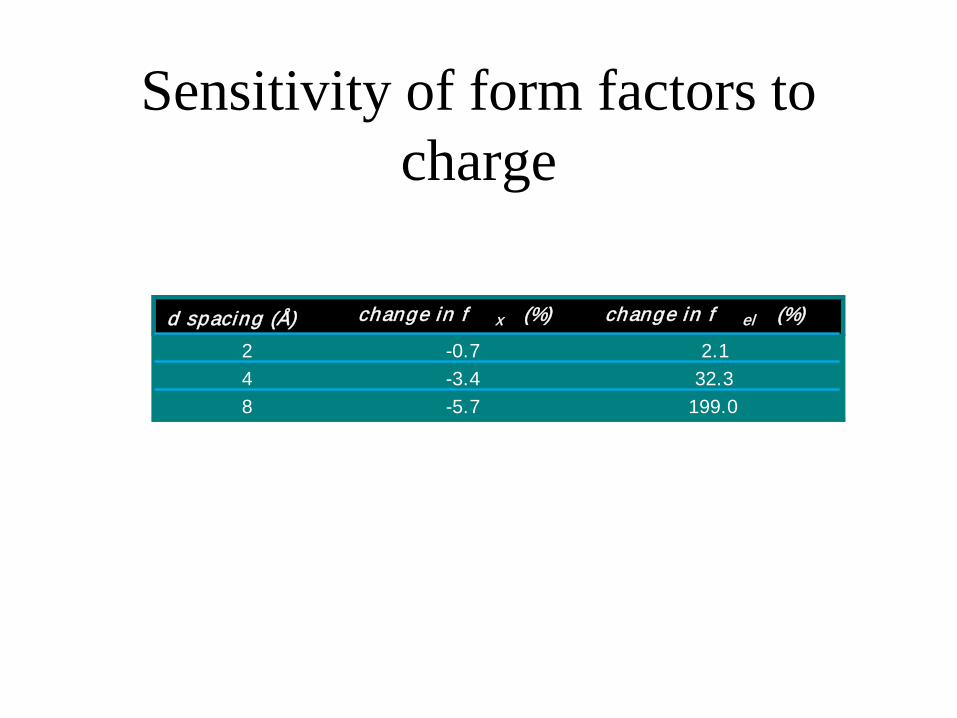
Sensitivity of form factors to charge
d spacing (Å) change in f x (%) change in f el (%)
2 -0.7 2.14 -3.4 32.38 -5.7 199.0
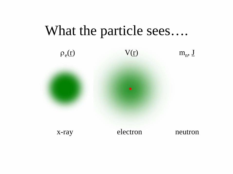
What the particle sees….
x-ray electron
ρe(r) V(r)
neutron
mn, J

Electron Form Factors
• Similar dependence on Z• At high angles - Rutherford-like
fel (k) = a Zk2
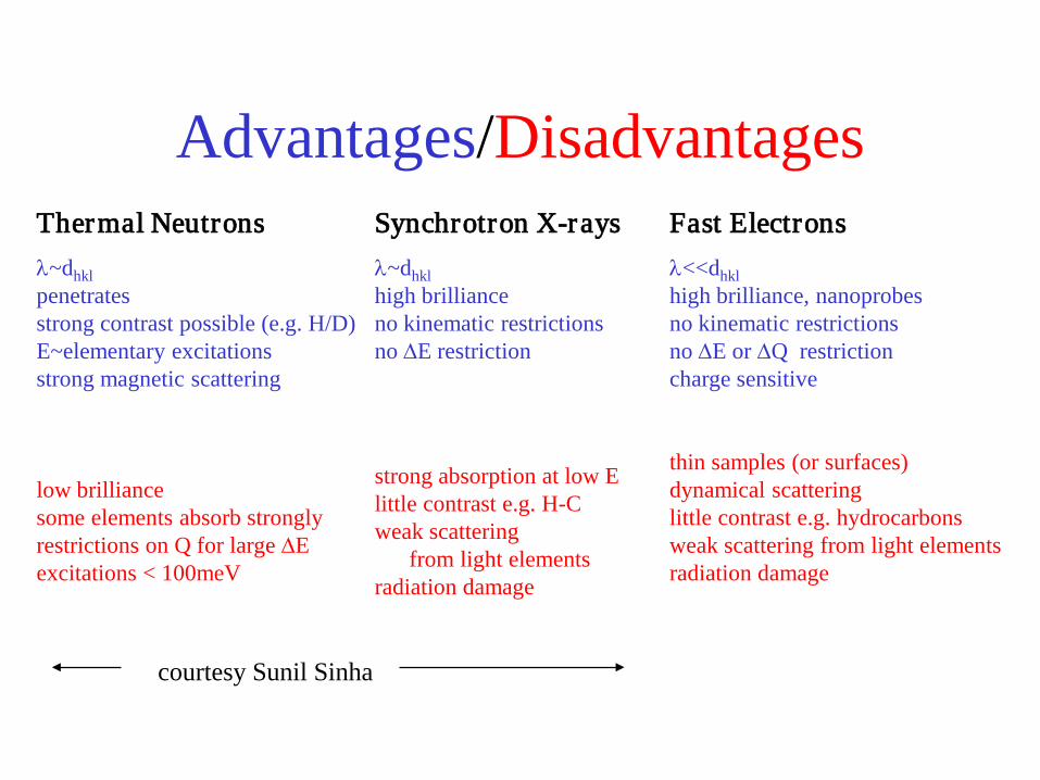
Advantages/DisadvantagesThermal Neutronsλ~dhklpenetratesstrong contrast possible (e.g. H/D)E~elementary excitationsstrong magnetic scattering
low brilliancesome elements absorb stronglyrestrictions on Q for large ∆Eexcitations < 100meV
Synchrotron X-raysλ~dhklhigh brillianceno kinematic restrictionsno ∆E restriction
strong absorption at low Elittle contrast e.g. H-Cweak scattering
from light elementsradiation damage
Fast Electronsλ<<dhklhigh brilliance, nanoprobesno kinematic restrictionsno ∆E or ∆Q restrictioncharge sensitive
thin samples (or surfaces)dynamical scatteringlittle contrast e.g. hydrocarbonsweak scattering from light elementsradiation damage
courtesy Sunil Sinha

Complementarity of techniques
Radiat ion SourceBrightness(part icles/cm2/steradian/eV)
Elast icMean-FreePath(Å)
Absorpt ionLength(Å)
M inimumProbe Size(Å)
Neut rons 1014 108 109 107
X-rays 1026 104 106 103
Elect rons 1029 102 103 1
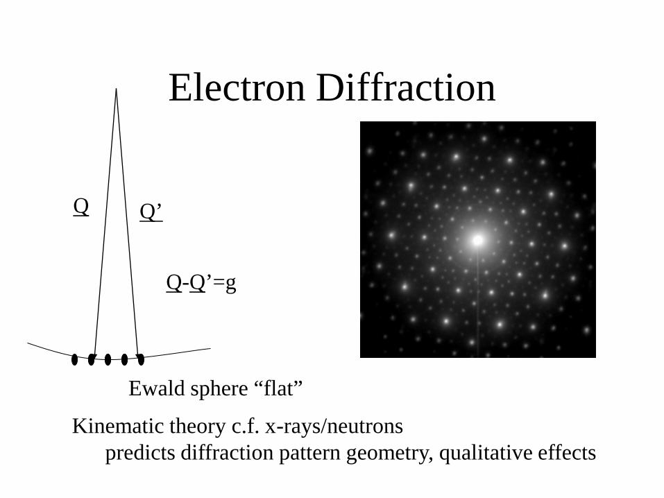
Electron Diffraction
Ewald sphere “flat”
Q Q’
Q-Q’=g
Kinematic theory c.f. x-rays/neutronspredicts diffraction pattern geometry, qualitative effects
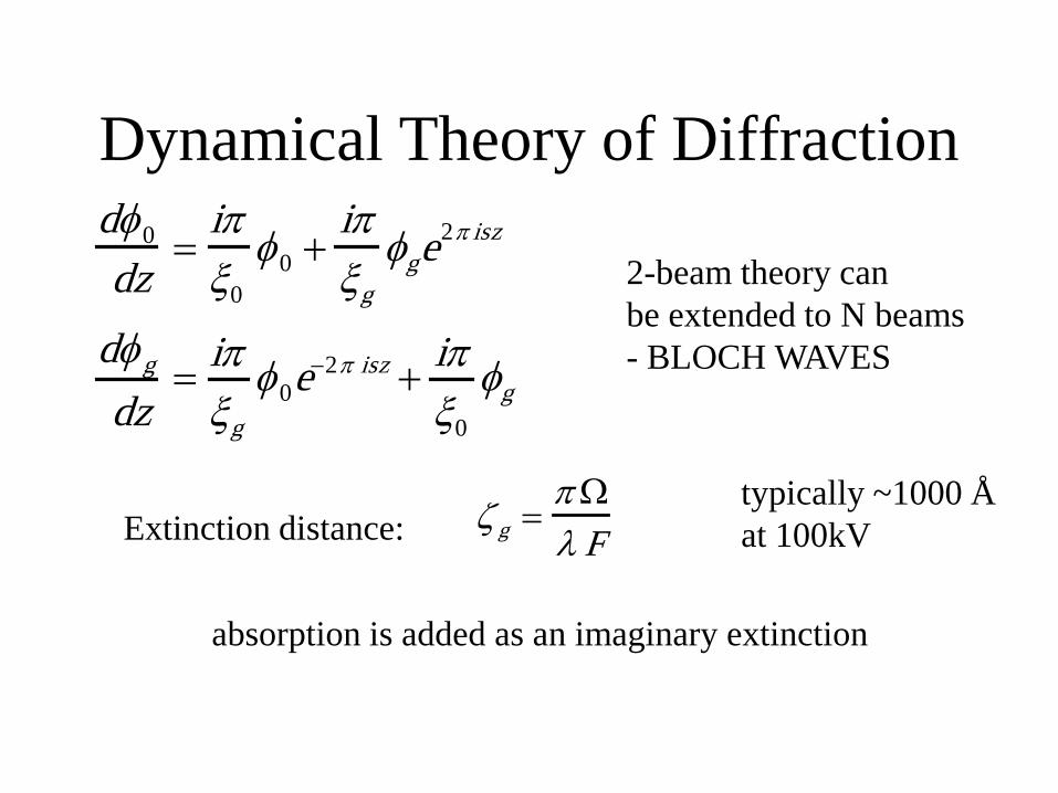
Dynamical Theory of Diffractiondφ0
dz=
iπξ0
φ0 +iπξg
φge2π isz
dφg
dz= iπ
ξg
φ0e−2π isz + iπξ0
φg
2-beam theory canbe extended to N beams- BLOCH WAVES
ζ g =π Ωλ FExtinction distance:
typically ~1000 Åat 100kV
absorption is added as an imaginary extinction
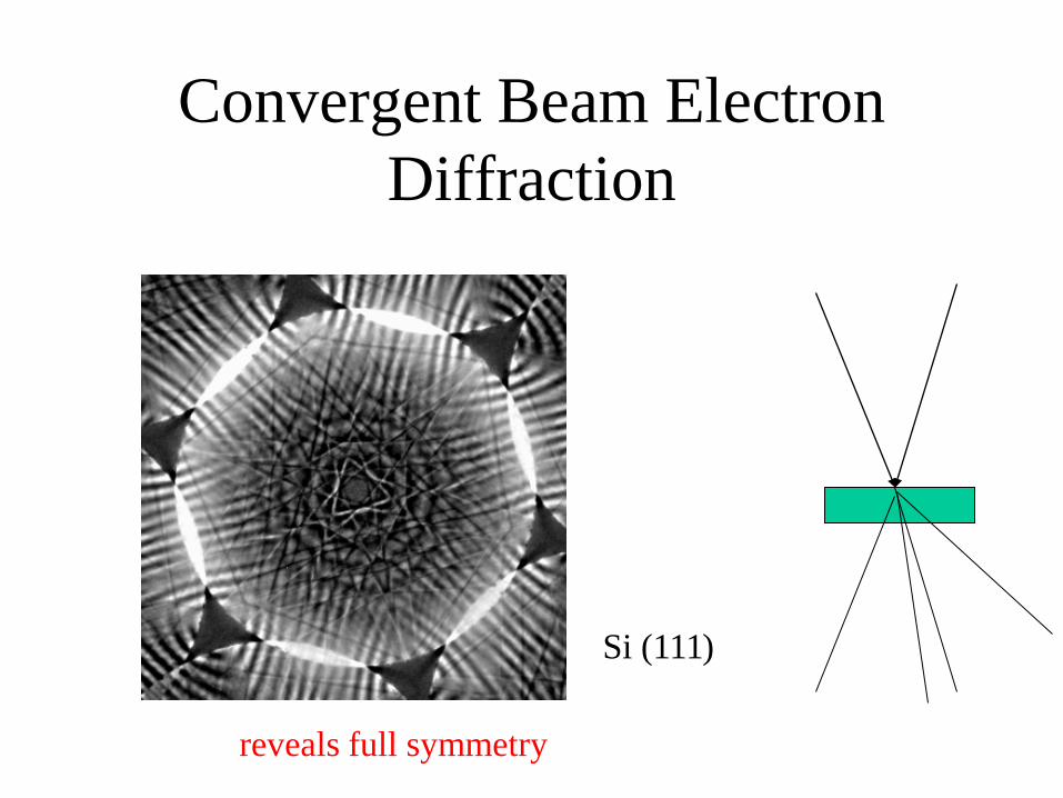
Convergent Beam Electron Diffraction
Si (111)
reveals full symmetry
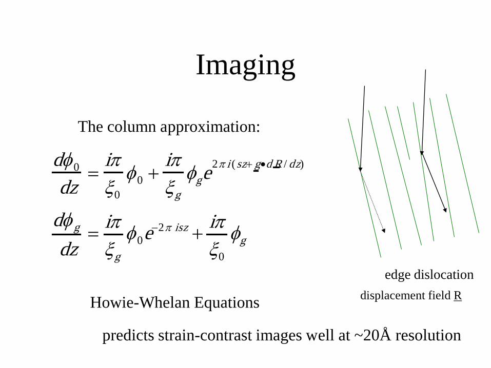
Imaging
The column approximation:
dφ0
dz=
iπξ0
φ0 +iπξg
φge2π i (sz+ g•d R / dz)
dφg
dz= iπ
ξg
φ0e−2π isz + iπξ0
φg
Howie-Whelan Equations
predicts strain-contrast images well at ~20Å resolution
edge dislocationdisplacement field R
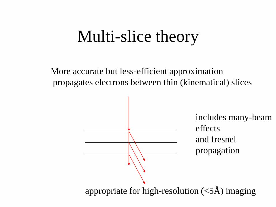
Multi-slice theory
More accurate but less-efficient approximationpropagates electrons between thin (kinematical) slices
includes many-beameffectsand fresnelpropagation
appropriate for high-resolution (<5Å) imaging
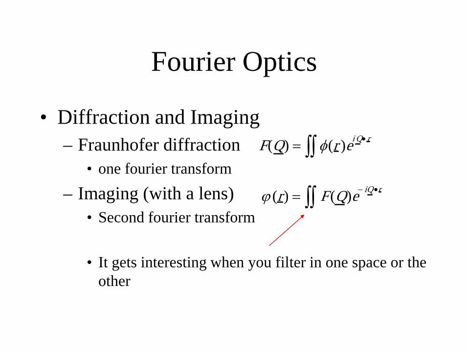
Fourier Optics
• Diffraction and Imaging– Fraunhofer diffraction
• one fourier transform– Imaging (with a lens)
• Second fourier transform
• It gets interesting when you filter in one space or the other
F(Q) = φ(r )ei Q• r∫∫
ϕ (r) = F(Q)e− iQ •r∫∫
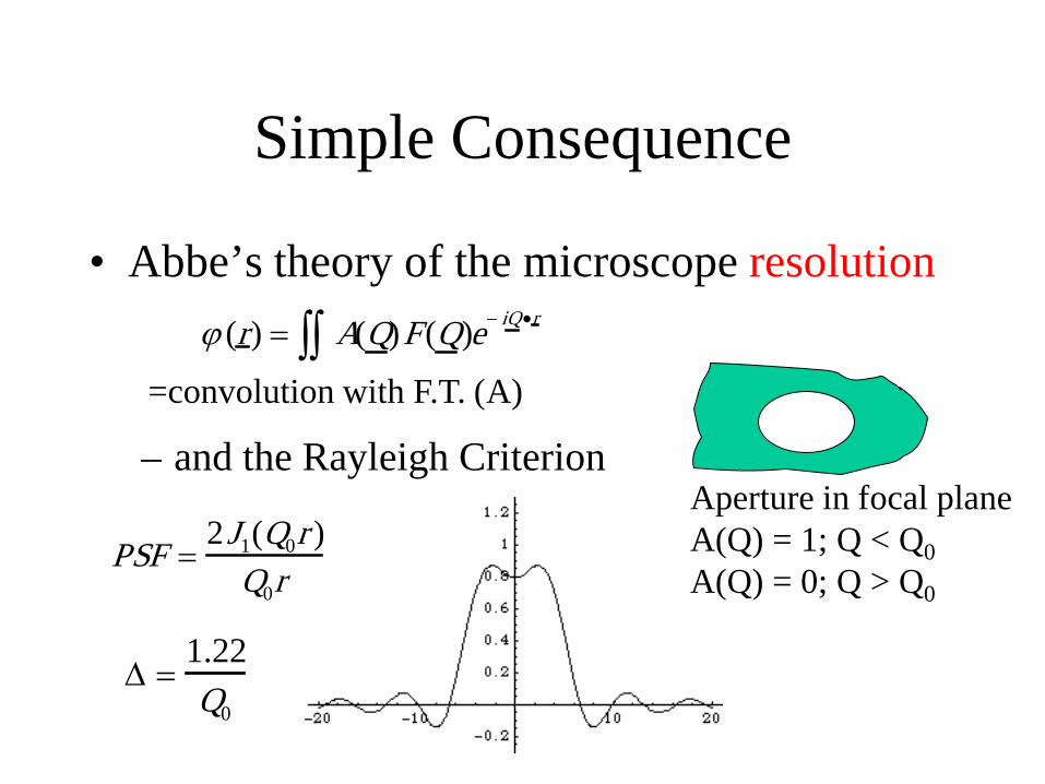
Simple Consequence
• Abbe’s theory of the microscope resolution
– and the Rayleigh Criterion
ϕ (r) = A(Q)F(Q)e− iQ •r∫∫=convolution with F.T. (A)
Aperture in focal planeA(Q) = 1; Q < Q0A(Q) = 0; Q > Q0
PSF =2J1(Q0r )
Q0r
∆ =1.22Q0
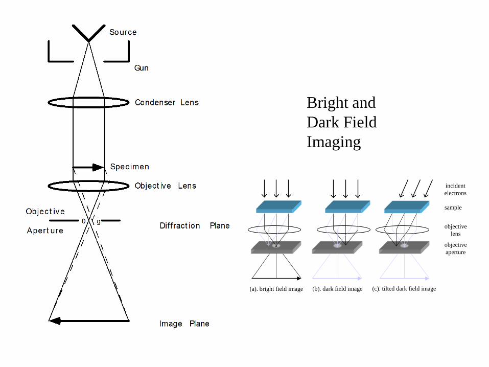
Bright andDark FieldImaging
(b). dark field image
incidentelectrons
sample
objectivelens
objectiveaperture
(a). bright field image (c). tilted dark field image
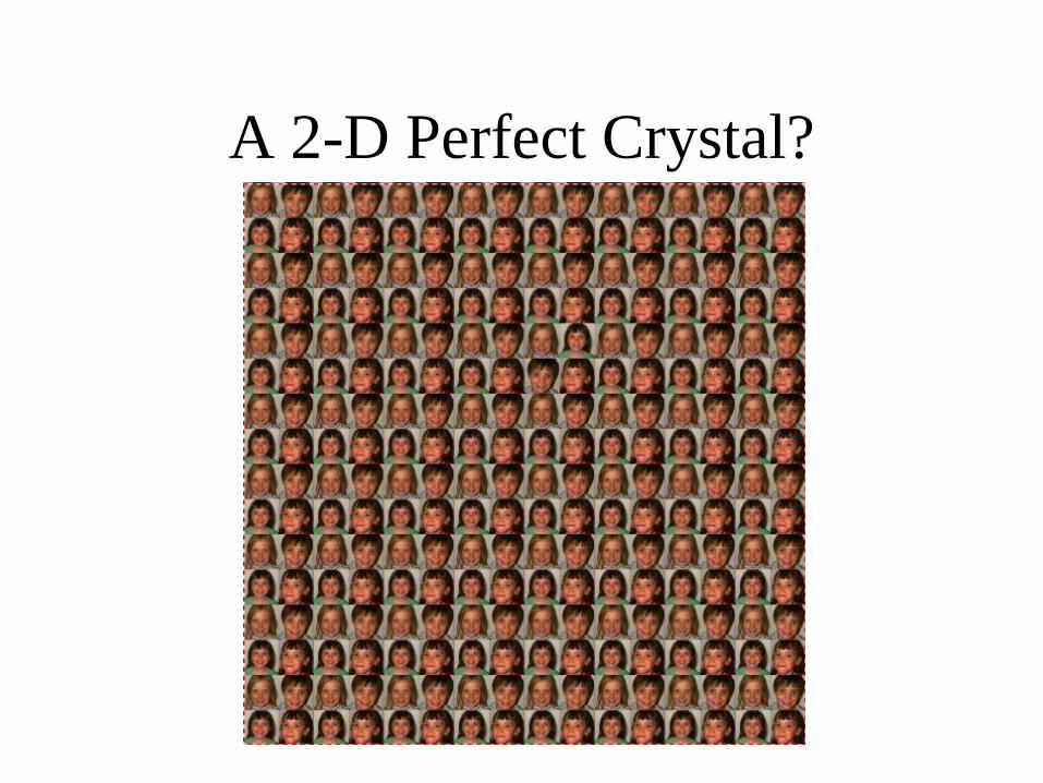
A 2-D Perfect Crystal?
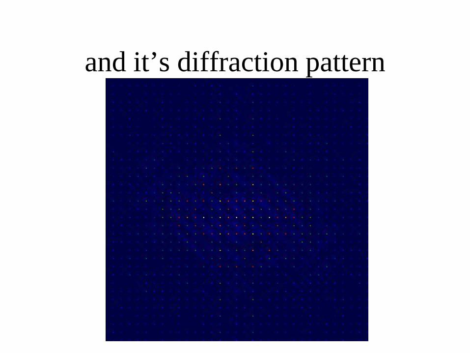
and it’s diffraction pattern
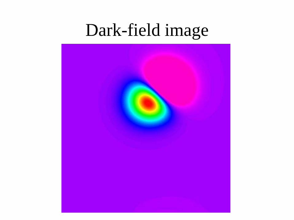
Dark-field image
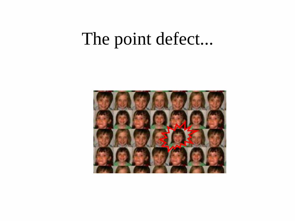
The point defect...
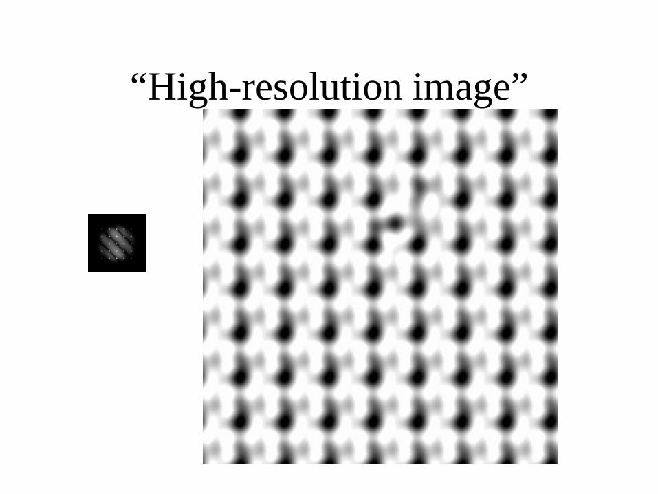
“High-resolution image”
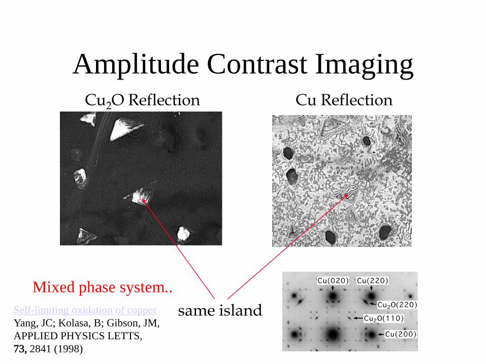
Cu2O Reflection Cu Reflection
same island
Amplitude Contrast Imaging
Mixed phase system..Self-limiting oxidation of copperYang, JC; Kolasa, B; Gibson, JM, APPLIED PHYSICS LETTS, 73, 2841 (1998)
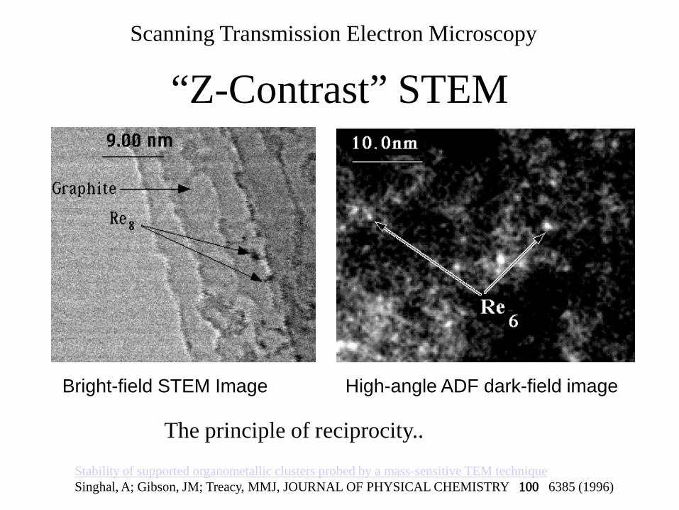
“Z-Contrast” STEM
Bright-field STEM Image High-angle ADF dark-field image
Scanning Transmission Electron Microscopy
The principle of reciprocity..
Stability of supported organometallic clusters probed by a mass-sensitive TEM techniqueSinghal, A; Gibson, JM; Treacy, MMJ, JOURNAL OF PHYSICAL CHEMISTRY 100 6385 (1996)
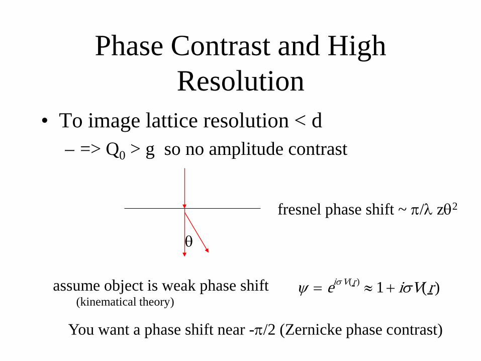
Phase Contrast and High Resolution
• To image lattice resolution < d– => Q0 > g so no amplitude contrast
θ
fresnel phase shift ~ π/λ zθ2
assume object is weak phase shift ψ = eiσV(r) ≈ 1 + iσV(r)(kinematical theory)
You want a phase shift near -π/2 (Zernicke phase contrast)
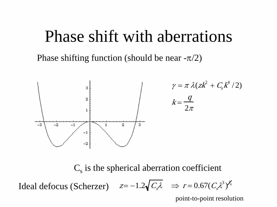
Phase shift with aberrationsPhase shifting function (should be near -π/2)
γ = π λ(zk2 + Cs k4 / 2)
k =q
2π
Cs is the spherical aberration coefficient
Ideal defocus (Scherzer) z = −1.2 Csλ ⇒ r = 0.67(Csλ3 )
14
point-to-point resolution

State of the art high-resolution
this picture shows reconstructed electronwavefunction revealing split Ga/N atoms
removing the microscopeaberrations - wavefront reconstruction,aberration correction
GaN (LBL)
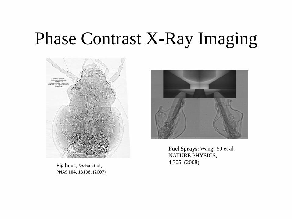
Phase Contrast X-Ray Imaging
Big bugs, Socha et al.,PNAS 104, 13198, (2007)
Fuel Sprays: Wang, YJ et al. NATURE PHYSICS, 4 305 (2008)
Examples
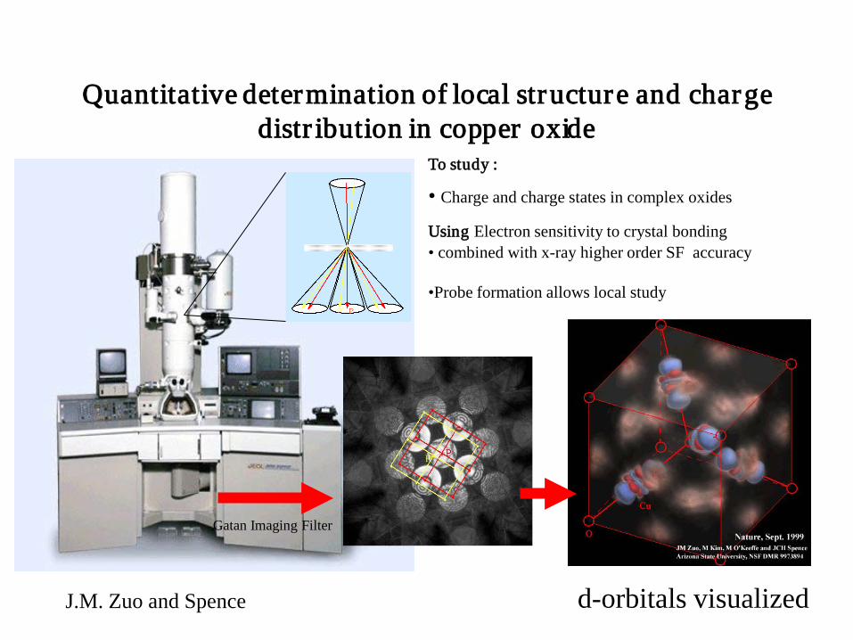
Quantitative determination of local structure and charge distr ibution in copper oxide
Gatan Imaging Filter
J.M. Zuo and Spence
To study :
• Charge and charge states in complex oxides
Using Electron sensitivity to crystal bonding• combined with x-ray higher order SF accuracy
•Probe formation allows local study
d-orbitals visualized
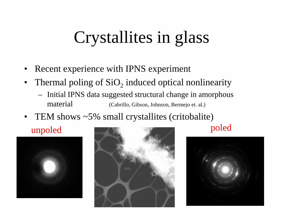
Crystallites in glass
• Recent experience with IPNS experiment• Thermal poling of SiO2 induced optical nonlinearity
– Initial IPNS data suggested structural change in amorphous material (Cabrillo, Gibson, Johnson, Bermejo et. al.)
• TEM shows ~5% small crystallites (critobalite)unpoled poled
Role of microscopy in confirming homogeneity
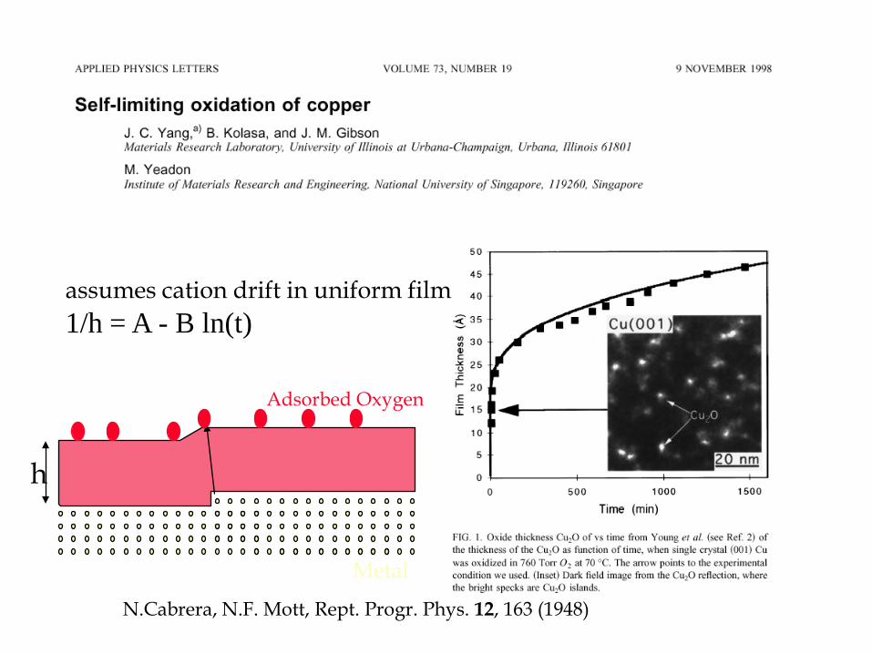
Metal
Adsorbed Oxygen
N.Cabrera, N.F. Mott, Rept. Progr. Phys. 12, 163 (1948)
h
assumes cation drift in uniform film1/h = A - B ln(t)
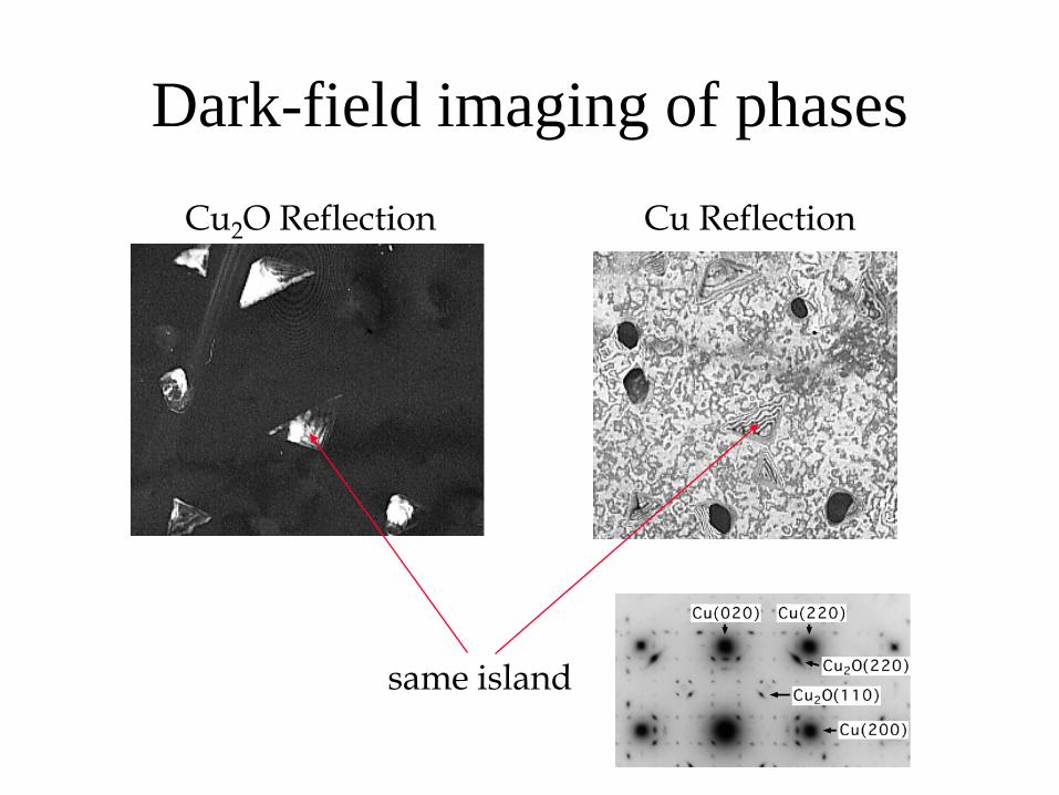
Dark-field imaging of phasesCu2O Reflection Cu Reflection
same island
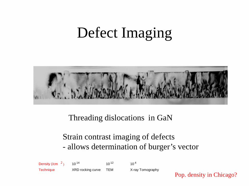
Defect Imaging
Threading dislocations in GaN
Strain contrast imaging of defects - allows determination of burger’s vector
Density (/cm 10 14 10 12 10 4
Technique XRD rocking curve TEM X-ray Tomography
2 )
Pop. density in Chicago?
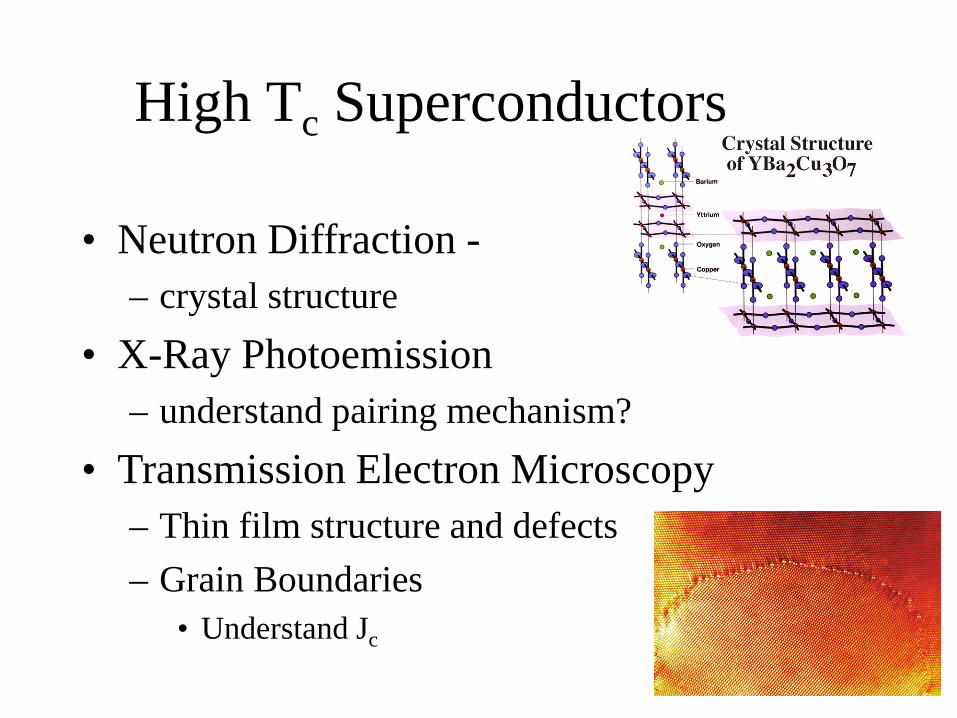
High Tc Superconductors
• Neutron Diffraction -– crystal structure
• X-Ray Photoemission– understand pairing mechanism?
• Transmission Electron Microscopy– Thin film structure and defects– Grain Boundaries
• Understand Jc
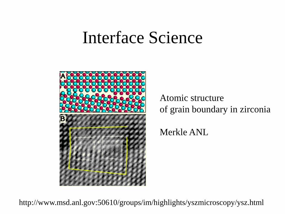
Atomic structureof grain boundary in zirconia
Merkle ANL
http://www.msd.anl.gov:50610/groups/im/highlights/yszmicroscopy/ysz.html
Interface Science
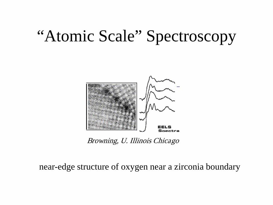
“Atomic Scale” Spectroscopy
Browning, U. Illinois Chicago
near-edge structure of oxygen near a zirconia boundary
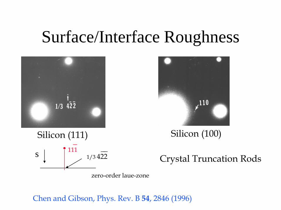
Surface/Interface Roughness
Silicon (111) Silicon (100)
zero-order laue-zone
1111/3 422 Crystal Truncation Rods
Chen and Gibson, Phys. Rev. B 54, 2846 (1996)
s
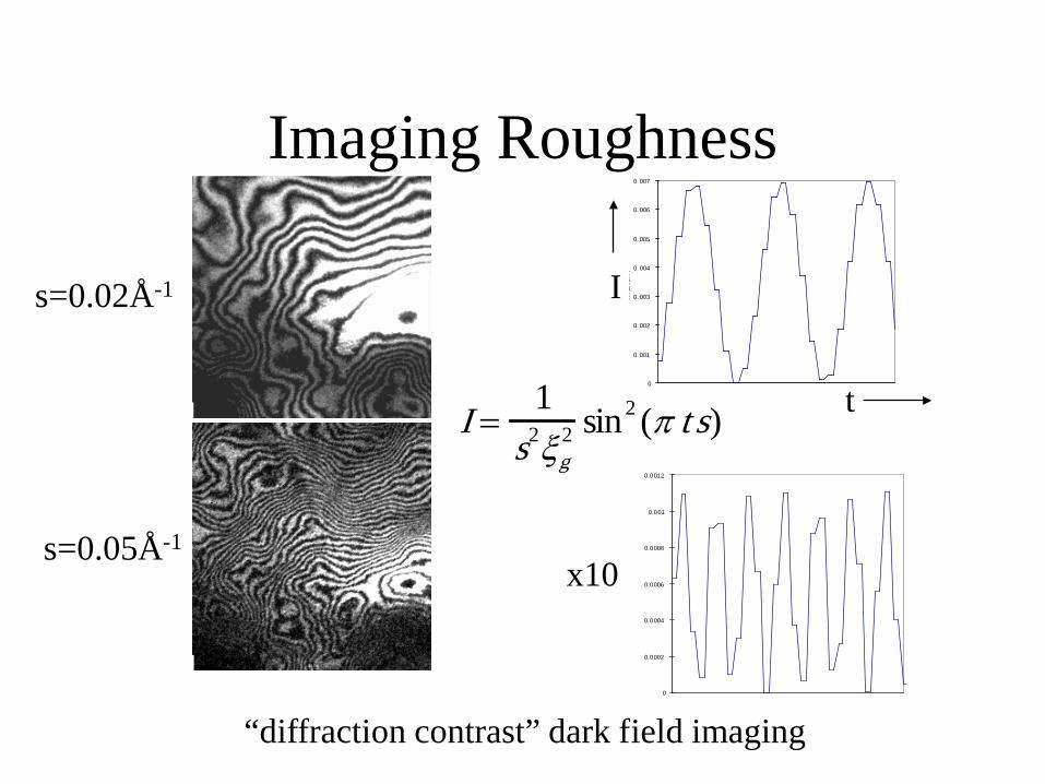
Imaging Roughness
s=0.02Å-1
s=0.05Å-1
0
0. 001
0. 002
0. 003
0. 004
0. 005
0. 006
0. 007
INT
EN
SIT
Y
0
0.0002
0.0004
0.0006
0.0008
0.001
0.0012
I =1
s2ξg2 sin2 (π t s)
x10
I
t
“diffraction contrast” dark field imaging
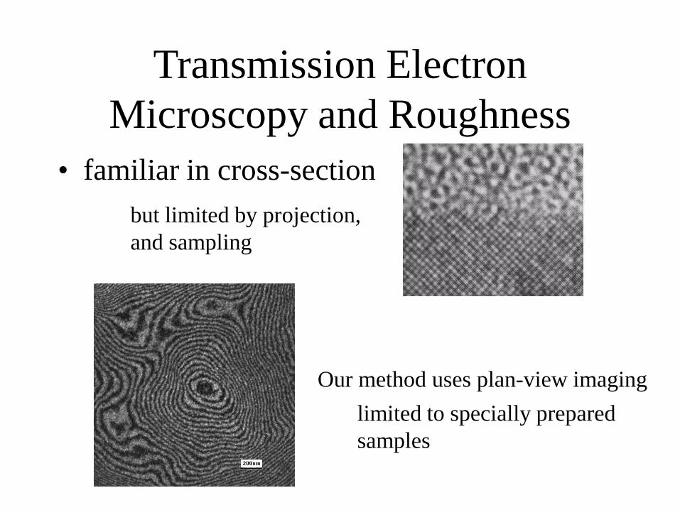
Transmission Electron Microscopy and Roughness
• familiar in cross-sectionbut limited by projection,and sampling
Our method uses plan-view imaginglimited to specially preparedsamples
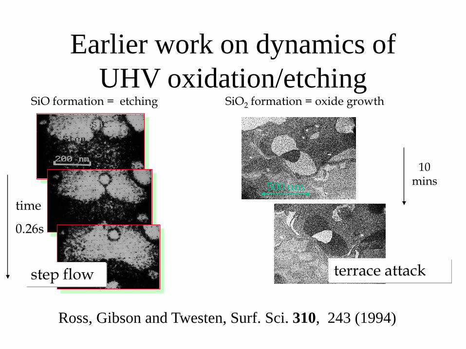
Earlier work on dynamics of UHV oxidation/etching
time
0.26s
SiO formation = etching
500 nm
SiO2 formation = oxide growth
step flow terrace attack
10mins
Ross, Gibson and Twesten, Surf. Sci. 310, 243 (1994)
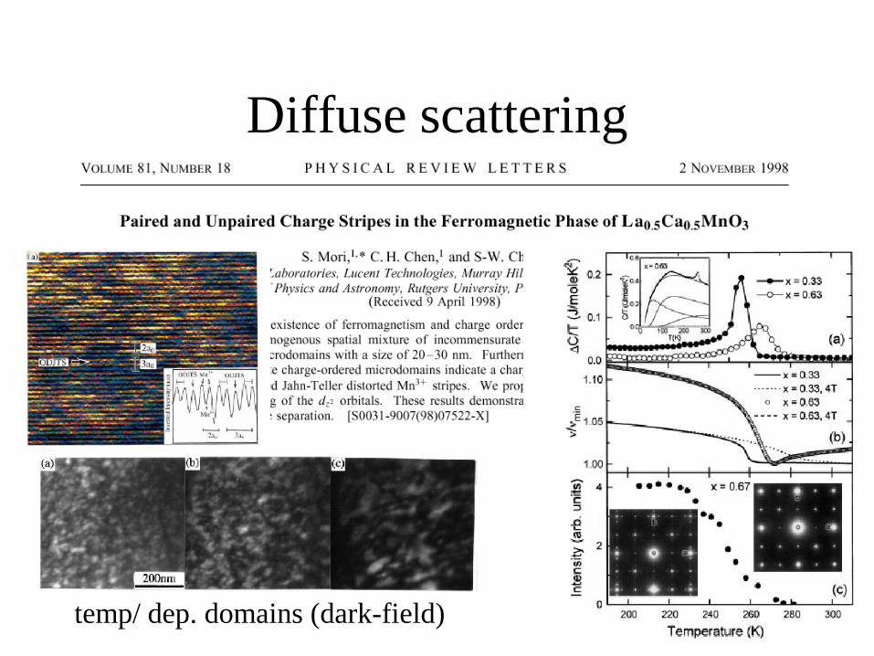
Diffuse scattering
temp/ dep. domains (dark-field)
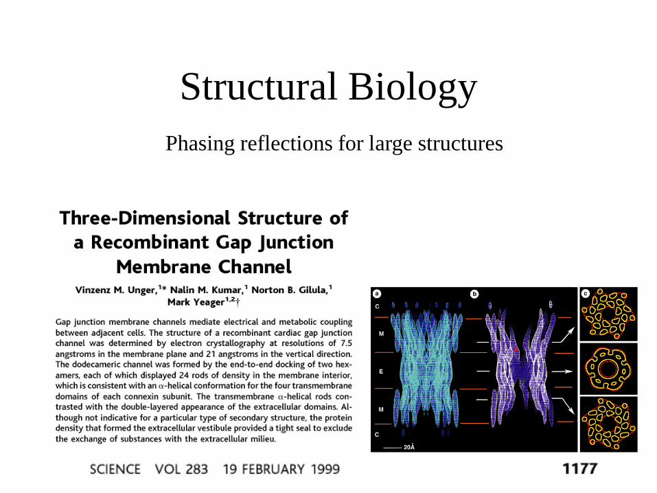
Structural BiologyPhasing reflections for large structures

x-ray structure this year depended on 7.5 Å e-structure

Nanoscience
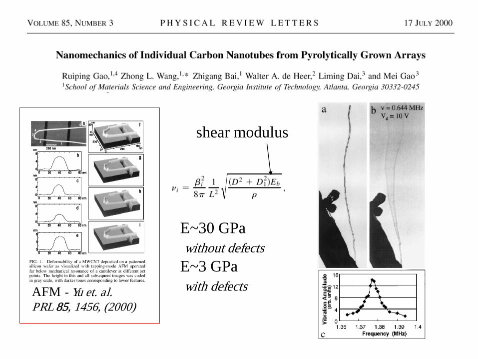
shear modulus
E~30 GPawithout defectsE~3 GPawith defectsAFM - Yu et. al.
PRL 85, 1456, (2000)
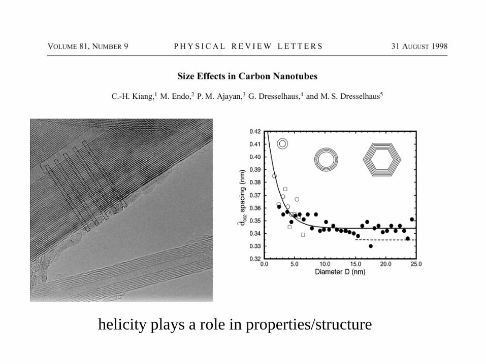
helicity plays a role in properties/structure
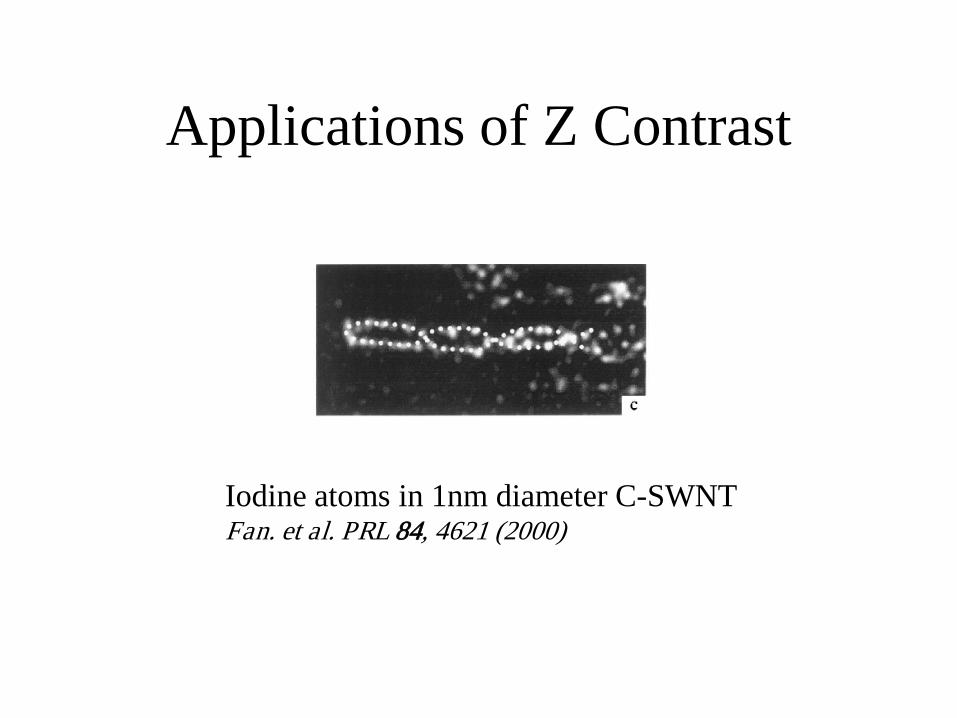
Applications of Z Contrast
Iodine atoms in 1nm diameter C-SWNTFan. et al. PRL 84, 4621 (2000)
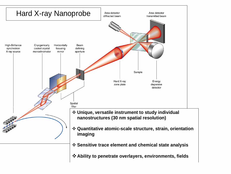
Unique, versatile instrument to study individualnanostructures (30 nm spatial resolution)
Quantitative atomic-scale structure, strain, orientationimaging
Sensitive trace element and chemical state analysis
Ability to penetrate overlayers, environments, fields
Hard X-ray Nanoprobe
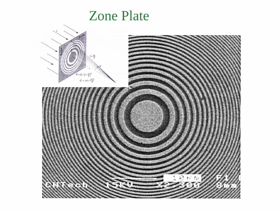
Zone Plate
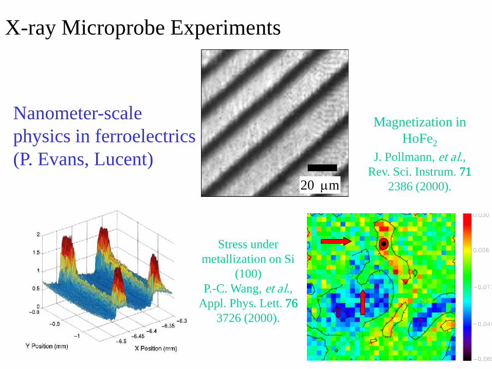
X-ray Microprobe Experiments
Nanometer-scale physics in ferroelectrics(P. Evans, Lucent)
20 µm
Magnetization in HoFe2
J. Pollmann, et al., Rev. Sci. Instrum. 71
2386 (2000).
Stress under metallization on Si
(100)P.-C. Wang, et al.,
Appl. Phys. Lett. 763726 (2000).

Nanoprobe diffraction studies of Nanopatterning - ETCHING
Microfocused beam will allow illumination of individual nanostructures.
Need to understand subtractive processes as well as additive (growth)
Novel materials will be investigated (e.g., multicomponent oxides).
- 6 - 4 - 2 0 2 4 6
- 1 0 0
- 5 0
0
5 0
1 0 0 7 0 n m x 7 0 n m
D C B i a s
hybridstructures
H. M. Christen et al., APL, 72 2535 (1998)
Studies of Growth and Etching

C. Thompson (NIU), S. Streiffer (ANL-MSD), A. McPherson (ANL-XFD)
Time-Resolved Studies of Ferroelectric Switching
VoltageCurrent
Lattice parameter during switching has been measured with 17 nsec time resolution.
Two-step response to voltage: prompt piezoresponse followed by switching on ~ 100 nsec time scale.
(+)
(-)
(-)
(+)
(-)
(+)
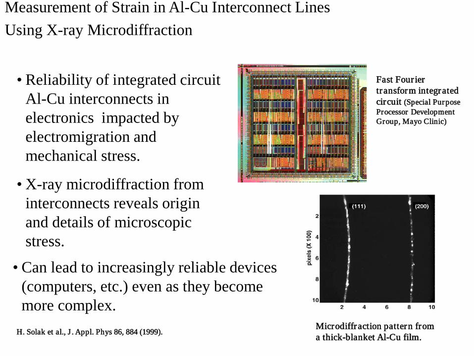
Measurement of Strain in Al-Cu Interconnect LinesUsing X-ray Microdiffraction
• Reliability of integrated circuit Al-Cu interconnects in electronics impacted by electromigration and mechanical stress.
• X-ray microdiffraction from interconnects reveals origin and details of microscopic stress.
Microdiffraction pattern from a thick-blanket Al-Cu film.
• Can lead to increasingly reliable devices (computers, etc.) even as they become more complex.
Fast Four ier transform integrated circuit (Special Purpose Processor Development Group, Mayo Clinic)
H. Solak et al., J . Appl. Phys 86, 884 (1999).
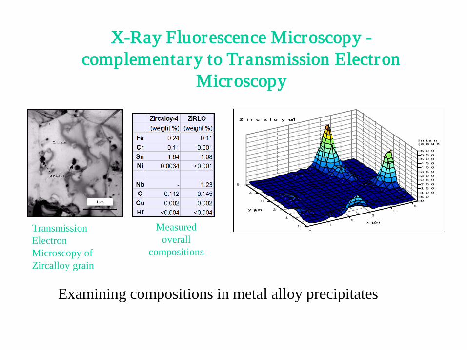
X-Ray Fluorescence Microscopy -complementary to Transmission Electron
Microscopy
Transmission ElectronMicroscopy of Zircalloy grain
Measured overall
compositions
01
23
45
0
1
2
3
4
5
05 01 0 01 5 02 0 02 5 03 0 03 5 04 0 04 5 05 0 05 5 06 0 0
i n t e n( c o u n
x (µm
y (µm
Z i r c a l o y - 4 α
Examining compositions in metal alloy precipitates
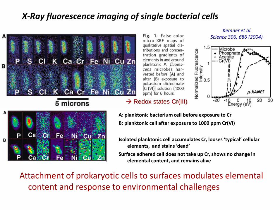
A: planktonic bacterium cell before exposure to Cr
B: planktonic cell after exposure to 1000 ppm Cr(VI)
Isolated planktonic cell accumulates Cr, looses ‘typical’ cellular elements, and stains ‘dead’
Surface adhered cell does not take up Cr, shows no change in elemental content, and remains alive
X-Ray fluorescence imaging of single bacterial cellsKemner et al.
Science 306, 686 (2004).
µ-XANES
Redox states Cr(III)
Attachment of prokaryotic cells to surfaces modulates elemental content and response to environmental challenges
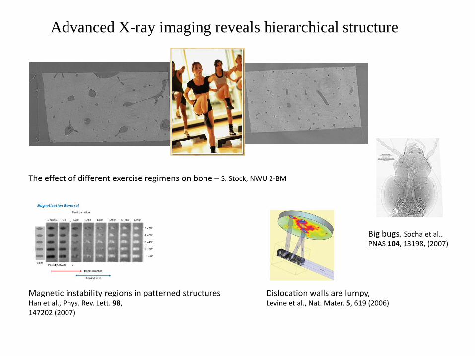
The effect of different exercise regimens on bone – S. Stock, NWU 2-BM
Advanced X-ray imaging reveals hierarchical structure
Magnetic instability regions in patterned structuresHan et al., Phys. Rev. Lett. 98,147202 (2007)
Big bugs, Socha et al.,PNAS 104, 13198, (2007)
Dislocation walls are lumpy,Levine et al., Nat. Mater. 5, 619 (2006)

Coherent X-Ray Diffraction Imaging
Analogous to crystallography Miao et al. (1999)
Coherent diffraction imaging is much like crystallography but applied to noncrystalline materials
First proposed by David Sayre in 1980, and first experimental demonstration by John Miao et al in 1999 using soft x-rays
Requires a fully coherent x-ray beam
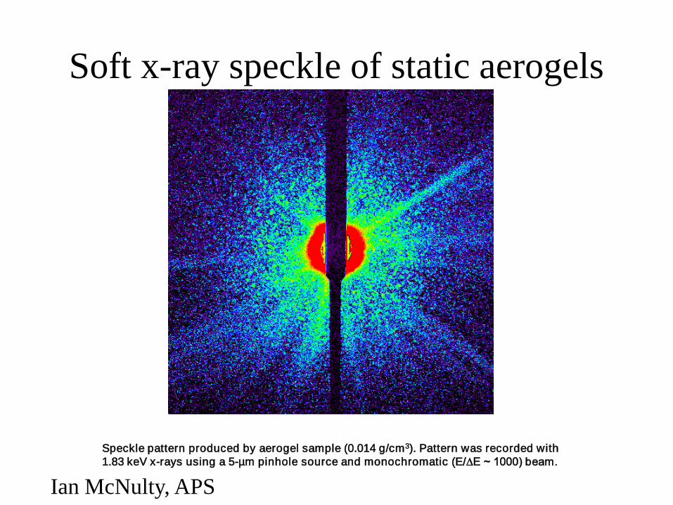
Soft x-ray speckle of static aerogels
Speckle pattern produced by aerogel sample (0.014 g/cm3). Pattern was recorded with1.83 keV x-rays using a 5-µm pinhole source and monochromatic (E/∆E ~ 1000) beam.
Ian McNulty, APS
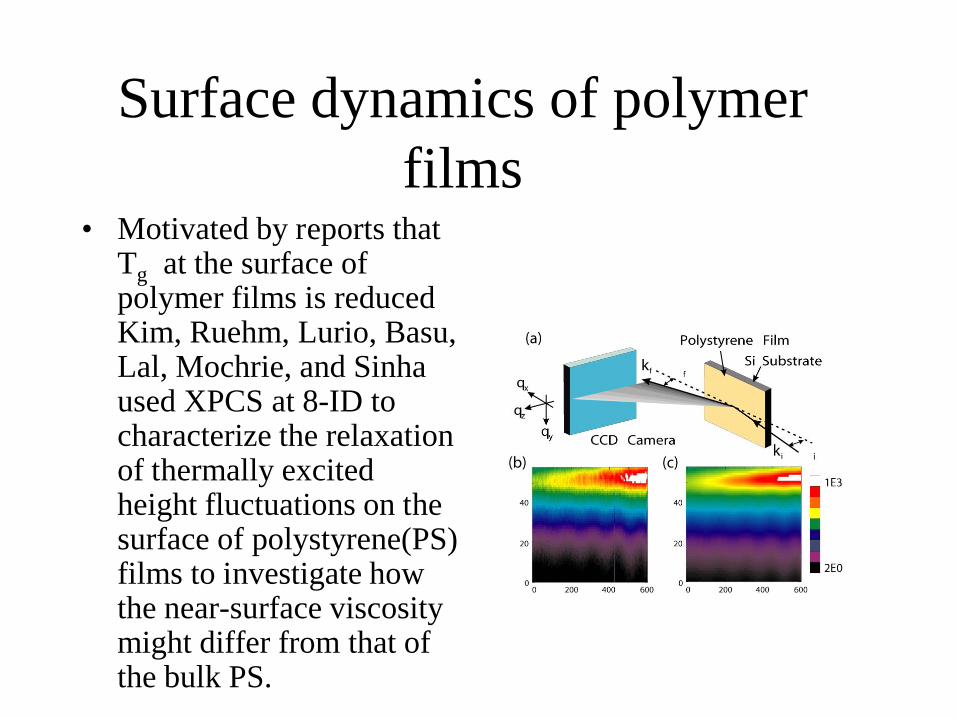
Surface dynamics of polymer films
• Motivated by reports that Tg at the surface of polymer films is reduced Kim, Ruehm, Lurio, Basu, Lal, Mochrie, and Sinha used XPCS at 8-ID to characterize the relaxation of thermally excited height fluctuations on the surface of polystyrene(PS) films to investigate how the near-surface viscosity might differ from that of the bulk PS.

Surface Dynamics of Polymer Films
Intensity correlation of the reveals the characteristic relaxation times for capillary waves
Shows nochange in Tgnear surface
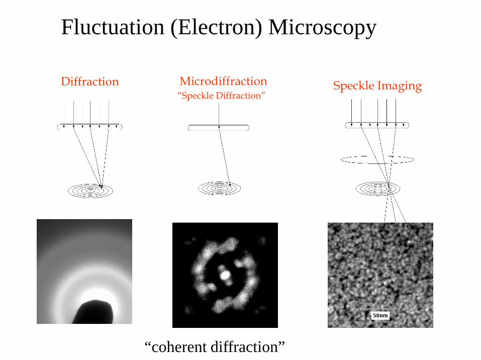
Fluctuation (Electron) Microscopy
Diffraction Microdiffraction Speckle Imaging“Speckle Diffraction”
“coherent diffraction”
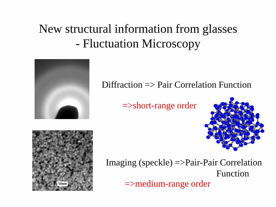
New structural information from glasses- Fluctuation Microscopy
Diffraction => Pair Correlation Function
Imaging (speckle) =>Pair-Pair Correlation Function
=>short-range order
=>medium-range order
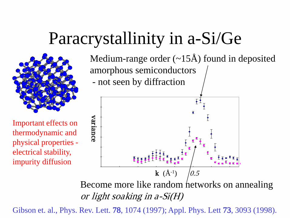
Paracrystallinity in a-Si/GeMedium-range order (~15Å) found in deposited amorphous semiconductors- not seen by diffraction
As-depositedAnnealed 350C
k (Å-1) 0.5
varianceBecome more like random networks on annealingor light soaking in a-Si(H)
Important effects on thermodynamic and physical properties -electrical stability, impurity diffusion
Gibson et. al., Phys. Rev. Lett. 78, 1074 (1997); Appl. Phys. Lett 73, 3093 (1998).

Further Reading
• “Electron Microscopy of Thin Crystals”, Hirsch et. al. (Kreiger, New York 1977)
• “Diffraction Physics”, J.M. Cowley, (North Holland, Amsterdam 1981)
• “Transmission Electron Microscopy”, L. Reimer, (Springer-Verlag, Berlin 1984)
• “Transmission Electron Microscopy: A Textbook for Mater ials Science”, D.B. Williams and C.B. Carter, (Plenum, New York 1996)