Supplementary Materials for -...
24
advances.sciencemag.org/cgi/content/full/4/3/eaaq0118/DC1 Supplementary Materials for Surface-agnostic highly stretchable and bendable conductive MXene multilayers Hyosung An, Touseef Habib, Smit Shah, Huili Gao, Miladin Radovic, Micah J. Green, Jodie L. Lutkenhaus Published 9 March 2018, Sci. Adv. 4, eaaq0118 (2018) DOI: 10.1126/sciadv.aaq0118 The PDF file includes: fig. S1. TEM image of a Ti3C2 MXene nanosheet on a perforated carbon grid. fig. S2. Digital images of (left) bare glass, (middle) the result of LbL assembly using only MXene sheets (without PDAC solution), and (right) 10-layer-pair MXene/PDAC multilayer coating. fig. S3. Adhesion testing with tape. fig. S4. A cross-sectional SEM image of the MXene multilayer prepared by spray- assisted LbL assembly on glass. fig. S5. AFM images of PDAC/MXene multilayers. fig. S6. Thickness of the multilayers as a function of the number of layer pairs. fig. S7. ATR-FTIR spectra of MXene, PDAC, and 20-layer-pair MXene multilayer coating. fig. S8. XPS survey spectra of MXene, (PDAC/MXene)20 multilayer finished with MXene, and (PDAC/MXene)20.5 multilayer finished with PDAC. fig. S9. XRD of MXene powder and multilayer. fig. S10. Digital images of MXene multilayers bending and stretching. fig. S11. Normalized resistance for bending and stretching. fig. S12. Comparison of resistance drift in literature. fig. S13. Images and normalized resistance of MXene multilayers on a variety of substrates. fig. S14. SEM images of MXene multilayers after bending and stretching. fig. S15. Geometric analysis of defects in bending. fig. S16. Geometric analysis of defects in stretching. fig. S17. A multilayer strain sensor. fig. S18. Strain versus the angle at the index finger.
-
Upload
truongmien -
Category
Documents
-
view
217 -
download
0
Transcript of Supplementary Materials for -...

advances.sciencemag.org/cgi/content/full/4/3/eaaq0118/DC1
Supplementary Materials for
Surface-agnostic highly stretchable and bendable conductive
MXene multilayers
Hyosung An, Touseef Habib, Smit Shah, Huili Gao, Miladin Radovic, Micah J. Green, Jodie L. Lutkenhaus
Published 9 March 2018, Sci. Adv. 4, eaaq0118 (2018)
DOI: 10.1126/sciadv.aaq0118
The PDF file includes:
fig. S1. TEM image of a Ti3C2 MXene nanosheet on a perforated carbon grid.
fig. S2. Digital images of (left) bare glass, (middle) the result of LbL assembly
using only MXene sheets (without PDAC solution), and (right) 10-layer-pair
MXene/PDAC multilayer coating.
fig. S3. Adhesion testing with tape.
fig. S4. A cross-sectional SEM image of the MXene multilayer prepared by spray-
assisted LbL assembly on glass.
fig. S5. AFM images of PDAC/MXene multilayers.
fig. S6. Thickness of the multilayers as a function of the number of layer pairs.
fig. S7. ATR-FTIR spectra of MXene, PDAC, and 20-layer-pair MXene
multilayer coating.
fig. S8. XPS survey spectra of MXene, (PDAC/MXene)20 multilayer finished with
MXene, and (PDAC/MXene)20.5 multilayer finished with PDAC.
fig. S9. XRD of MXene powder and multilayer.
fig. S10. Digital images of MXene multilayers bending and stretching.
fig. S11. Normalized resistance for bending and stretching.
fig. S12. Comparison of resistance drift in literature.
fig. S13. Images and normalized resistance of MXene multilayers on a variety of
substrates.
fig. S14. SEM images of MXene multilayers after bending and stretching.
fig. S15. Geometric analysis of defects in bending.
fig. S16. Geometric analysis of defects in stretching.
fig. S17. A multilayer strain sensor.
fig. S18. Strain versus the angle at the index finger.
table S1. Atomic composition at the surface of cast MXene sheets,
(PDAC/MXene)20 multilayer terminated with MXene, and (PDAC/MXene)20.5
multilayer terminated with PDAC from XPS survey spectra (fig. S8).
table S2. Characteristics of flexible MXene-based films or coatings.
table S3. Characteristics of reported bendable conductors.
table S4. Characteristics of reported stretchable conductors.
Legends for movies S1 to S10
References (29–61)
Other Supplementary Material for this manuscript includes the following:
(available at advances.sciencemag.org/cgi/content/full/4/3/eaaq0118/DC1)
movie S1 (.mov format). A nylon fiber coated with a MXene multilayer, showing
conductive properties.
movie S2 (.mov format). An MXene multilayer on PET lights up a white LED
under folding.
movie S3 (.mov format). Cyclic bending of a MXene multilayer on PET shows
rapid and reversible response.
movie S4 (.mov format). An MXene multilayer on PET detects bending
deformations.
movie S5 (.mov format). A kirigami MXene multilayer on PET detects stretching
deformations.
movie S6 (.mov format). A kirigami pattern allows MXene multilayer–coated
PET to be stretchable.
movie S7 (.mov format). An MXene multilayer on PDMS detects stretching
deformations.
movie S8 (.mov format). An MXene multilayer on PDMS detects a twisting
deformation.
movie S9 (.mov format). A patterned multilayer strain sensor detects various
degrees of bending (0° to 40°) with rapid response.
movie S10 (.mov format). A topographic scanner was fabricated using a patterned
MXene multilayer–coated PET film.
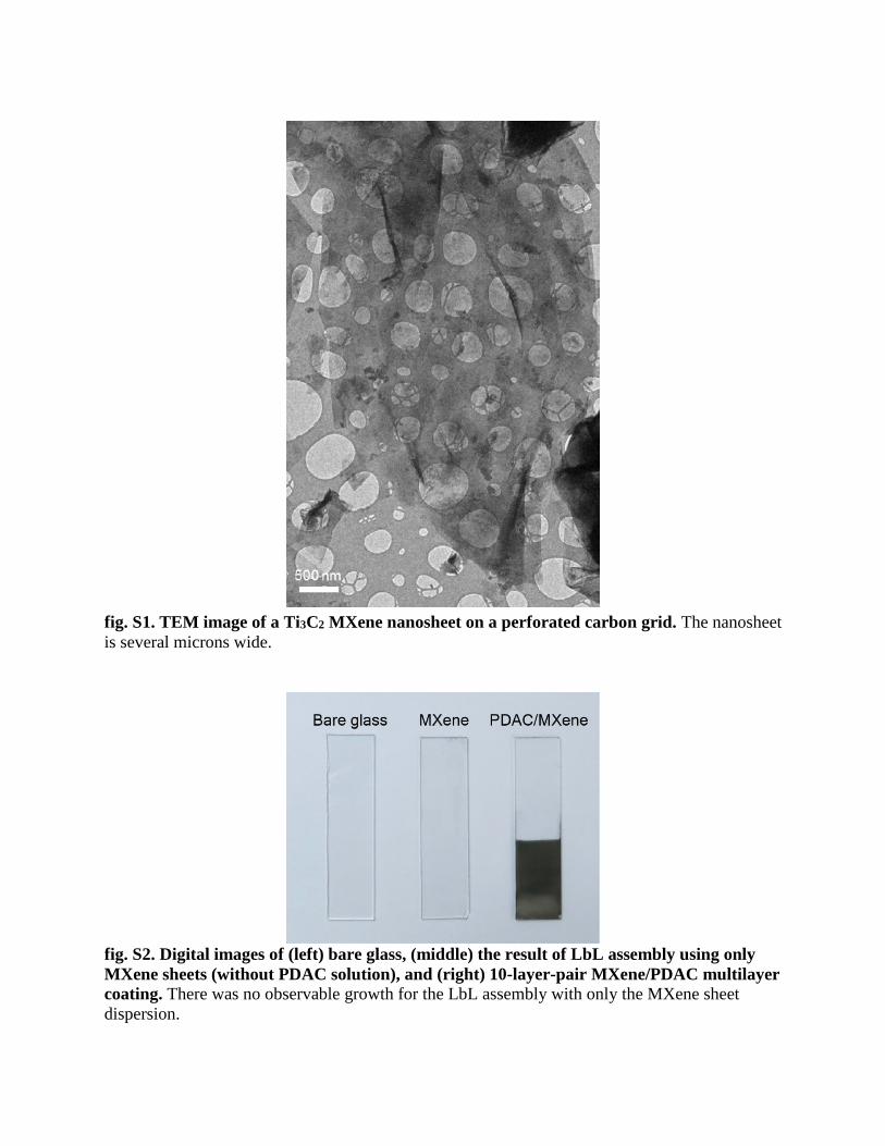
fig. S1. TEM image of a Ti3C2 MXene nanosheet on a perforated carbon grid. The nanosheet
is several microns wide.
fig. S2. Digital images of (left) bare glass, (middle) the result of LbL assembly using only
MXene sheets (without PDAC solution), and (right) 10-layer-pair MXene/PDAC multilayer
coating. There was no observable growth for the LbL assembly with only the MXene sheet
dispersion.
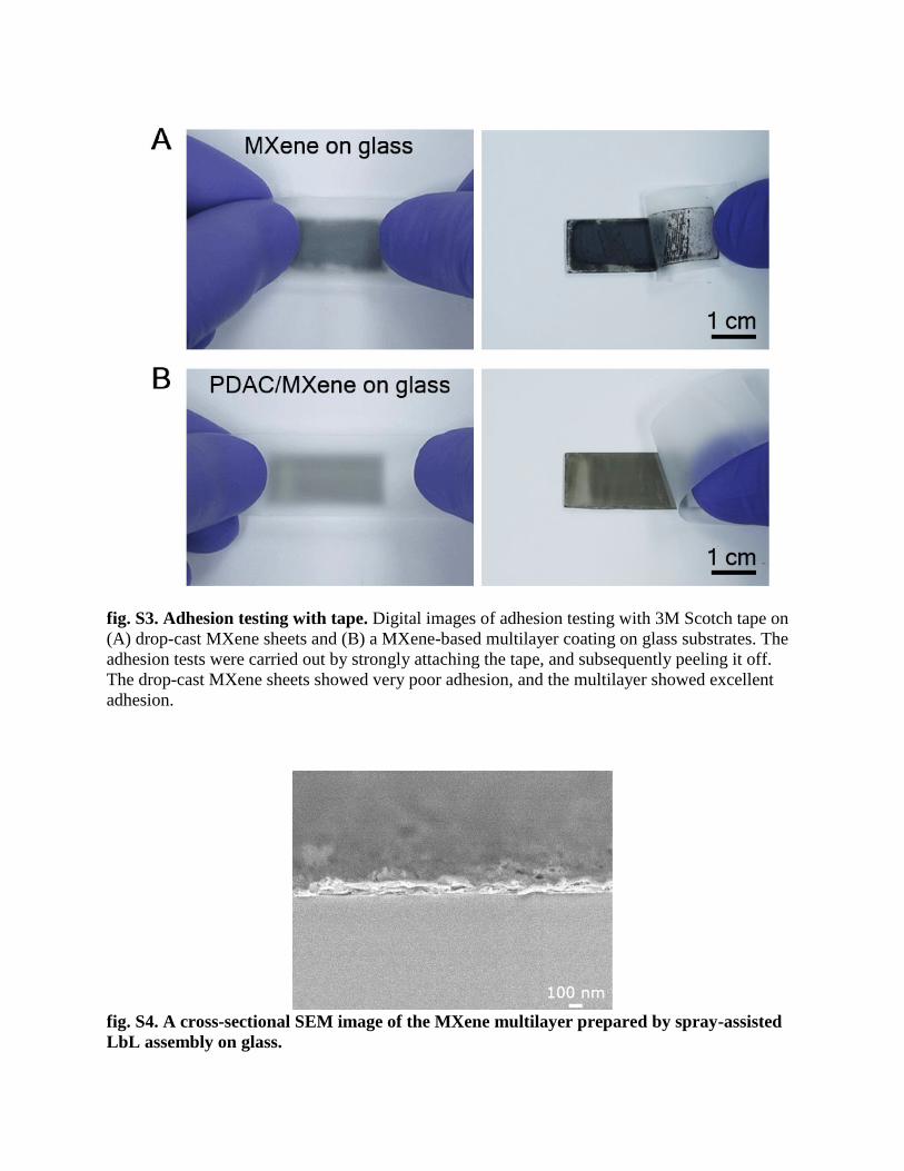
fig. S3. Adhesion testing with tape. Digital images of adhesion testing with 3M Scotch tape on
(A) drop-cast MXene sheets and (B) a MXene-based multilayer coating on glass substrates. The
adhesion tests were carried out by strongly attaching the tape, and subsequently peeling it off.
The drop-cast MXene sheets showed very poor adhesion, and the multilayer showed excellent
adhesion.
fig. S4. A cross-sectional SEM image of the MXene multilayer prepared by spray-assisted
LbL assembly on glass.
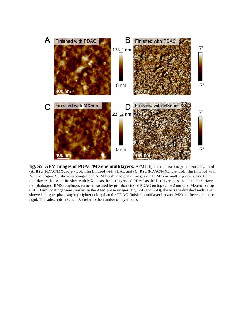
fig. S5. AFM images of PDAC/MXene multilayers. AFM height and phase images (2 μm × 2 μm) of
(A, B) a (PDAC/MXene)50.5 LbL film finished with PDAC and (C, D) a (PDAC/MXene)50 LbL film finished with
MXene. Figure S5 shows tapping-mode AFM height and phase images of the MXene multilayer on glass. Both
multilayers that were finished with MXene as the last layer and PDAC as the last layer possessed similar surface
morphologies. RMS roughness values measured by profilometry of PDAC on top (25 ± 2 nm) and MXene on top
(29 ± 3 nm) coatings were similar. In the AFM phase images (fig. S5B and S5D), the MXene-finished multilayer
showed a higher phase angle (brighter color) than the PDAC-finished multilayer because MXene sheets are more
rigid. The subscripts 50 and 50.5 refer to the number of layer pairs.
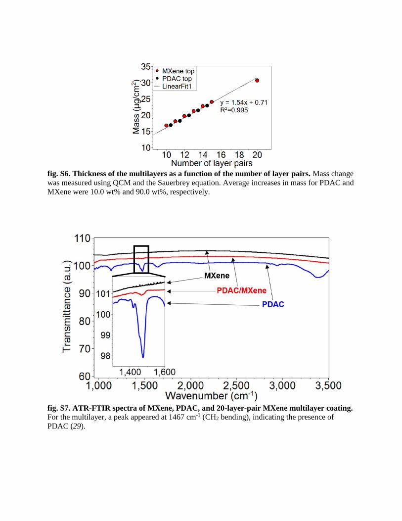
fig. S6. Thickness of the multilayers as a function of the number of layer pairs. Mass change
was measured using QCM and the Sauerbrey equation. Average increases in mass for PDAC and
MXene were 10.0 wt% and 90.0 wt%, respectively.
fig. S7. ATR-FTIR spectra of MXene, PDAC, and 20-layer-pair MXene multilayer coating. For the multilayer, a peak appeared at 1467 cm-1 (CH2 bending), indicating the presence of
PDAC (29).
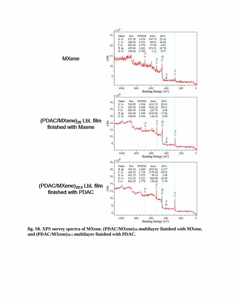
fig. S8. XPS survey spectra of MXene, (PDAC/MXene)20 multilayer finished with MXene,
and (PDAC/MXene)20.5 multilayer finished with PDAC.
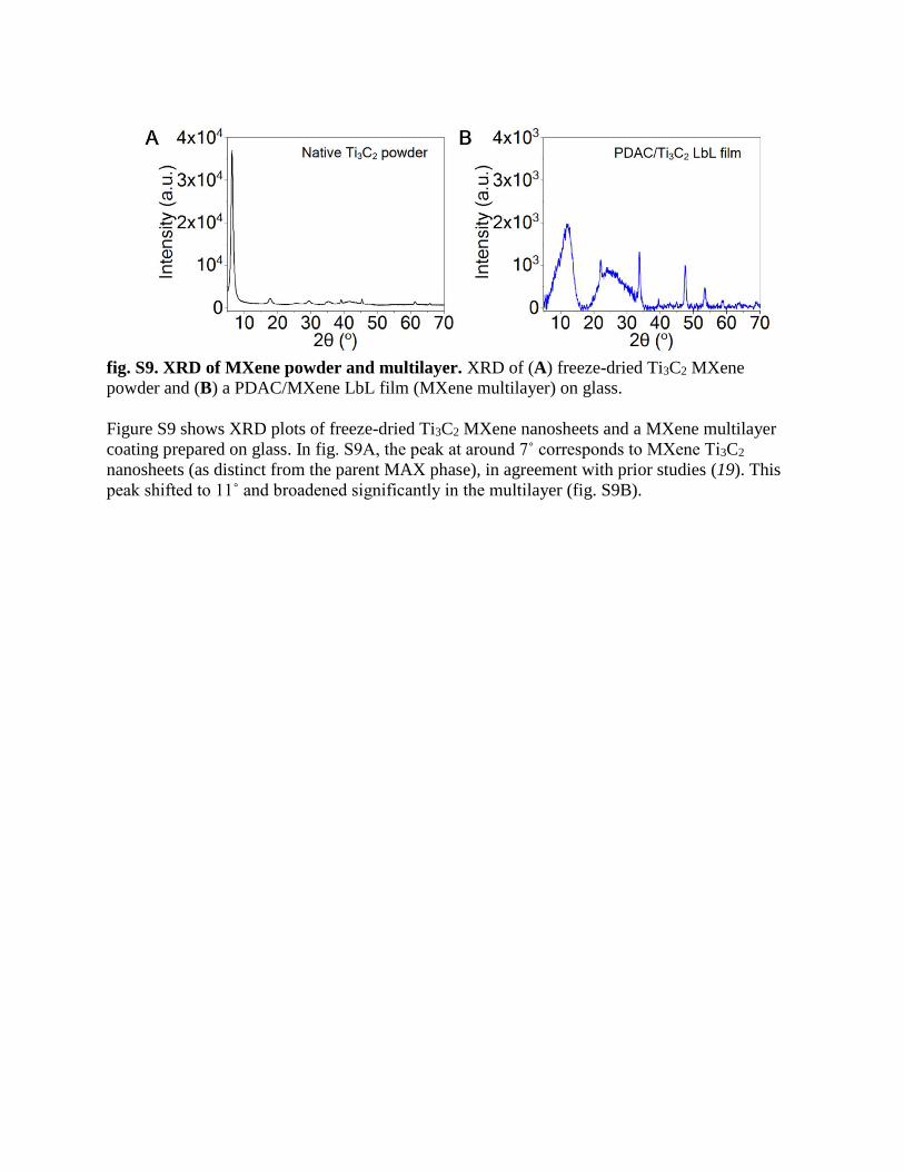
fig. S9. XRD of MXene powder and multilayer. XRD of (A) freeze-dried Ti3C2 MXene
powder and (B) a PDAC/MXene LbL film (MXene multilayer) on glass.
Figure S9 shows XRD plots of freeze-dried Ti3C2 MXene nanosheets and a MXene multilayer
coating prepared on glass. In fig. S9A, the peak at around 7˚ corresponds to MXene Ti3C2
nanosheets (as distinct from the parent MAX phase), in agreement with prior studies (19). This
peak shifted to 11˚ and broadened significantly in the multilayer (fig. S9B).
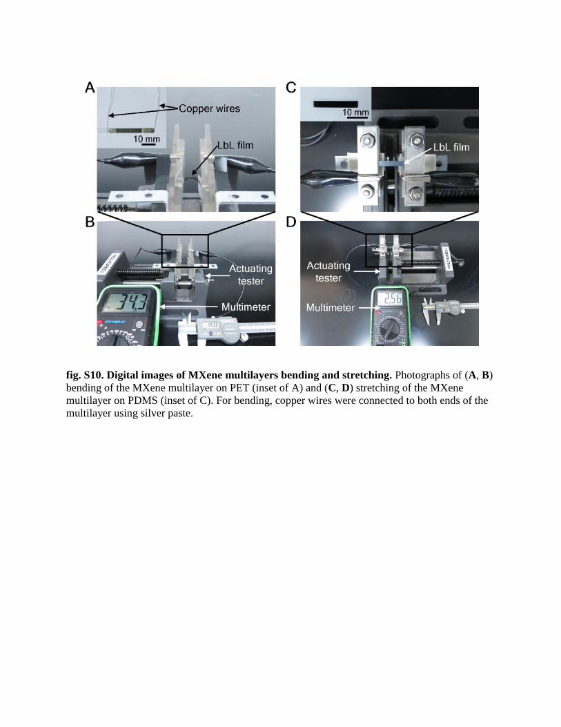
fig. S10. Digital images of MXene multilayers bending and stretching. Photographs of (A, B)
bending of the MXene multilayer on PET (inset of A) and (C, D) stretching of the MXene
multilayer on PDMS (inset of C). For bending, copper wires were connected to both ends of the
multilayer using silver paste.
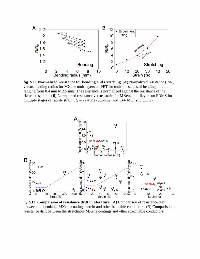
fig. S11. Normalized resistance for bending and stretching. (A) Normalized resistance (R/R0)
versus bending radius for MXene multilayers on PET for multiple stages of bending at radii
ranging from 8.4 mm to 2.5 mm. The resistance is normalized against the resistance of the
flattened sample. (B) Normalized resistance versus strain for MXene multilayers on PDMS for
multiple stages of tensile strain. R0 = 22.4 kΩ (bending) and 1.66 MΩ (stretching).
fig. S12. Comparison of resistance drift in literature. (A) Comparison of resistance drift
between the bendable MXene coatings herein and other bendable conductors. (B) Comparison of
resistance drift between the stretchable MXene coatings and other stretchable conductors.
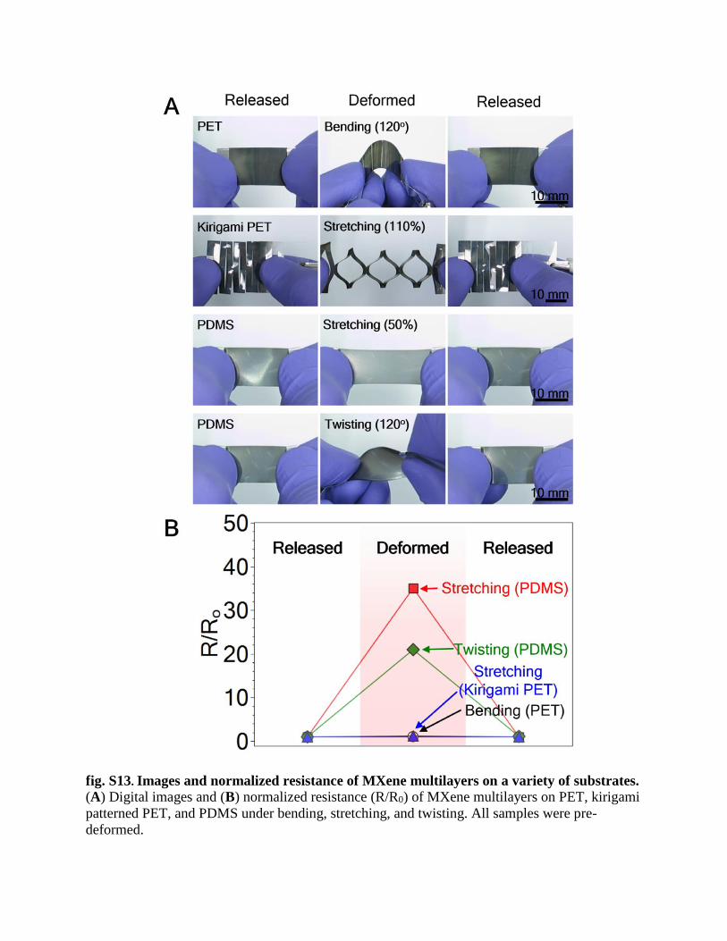
fig. S13. Images and normalized resistance of MXene multilayers on a variety of substrates.
(A) Digital images and (B) normalized resistance (R/R0) of MXene multilayers on PET, kirigami
patterned PET, and PDMS under bending, stretching, and twisting. All samples were pre-
deformed.
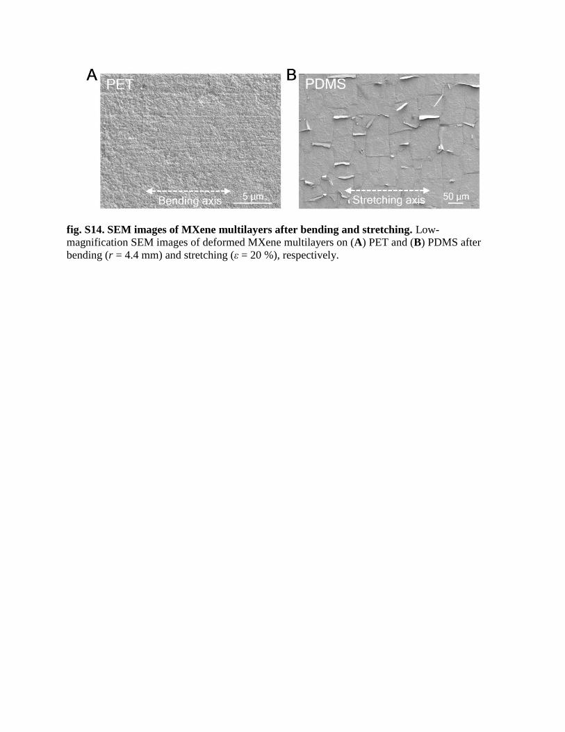
fig. S14. SEM images of MXene multilayers after bending and stretching. Low-
magnification SEM images of deformed MXene multilayers on (A) PET and (B) PDMS after
bending (r = 4.4 mm) and stretching (ε = 20 %), respectively.
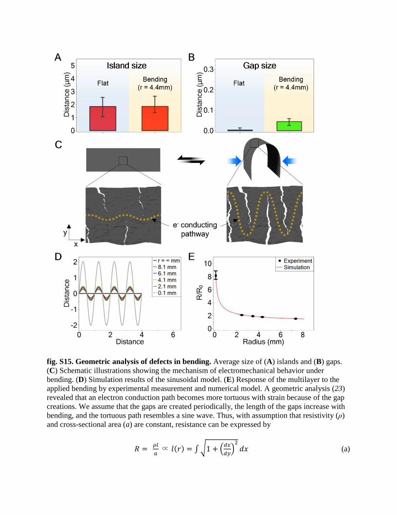
fig. S15. Geometric analysis of defects in bending. Average size of (A) islands and (B) gaps.
(C) Schematic illustrations showing the mechanism of electromechanical behavior under
bending. (D) Simulation results of the sinusoidal model. (E) Response of the multilayer to the
applied bending by experimental measurement and numerical model. A geometric analysis (23)
revealed that an electron conduction path becomes more tortuous with strain because of the gap
creations. We assume that the gaps are created periodically, the length of the gaps increase with
bending, and the tortuous path resembles a sine wave. Thus, with assumption that resistivity (ρ)
and cross-sectional area (a) are constant, resistance can be expressed by
𝑅 = 𝜌𝑙
𝑎 ∝ 𝑙(𝑟) = ∫√1 + (
𝑑𝑥
𝑑𝑦)2
𝑑𝑥 (a)
𝑦 = 𝐴 sin(𝐵𝑥) (b)
where ε is strain; x is variable; A is an amplitude which is a function of bending radius, f(r); and
B is a constant (i.e., 2π). Physically, an amplitude should increase with bending. A can be
determined by fitting to experimental data (fig. S15D).
𝐴 = 0.6854 r0.4661 (c)
Thus, by knowing A, equation y is shown to follow a power-law
𝑦 = 𝐴 sin(𝐵𝑥) = 0.6854 r0.4661 sin(2𝜋𝑥) (d)
Because equation (a) does not have an analytical solution, it should be solved numerically. The
numerical solution of l and relative resistance are below
𝑙 = 𝑙𝑜3.0537r0.365 (e)
𝑅
𝑅𝑜=
𝑙
𝑙𝑜= 3.0537r0.365 (f)
where lo is the initial length of the film, and Ro is the initial resistance. The excellent agreement
between the model and experiment (fig. S15E) allows us to gauge the resistance dependence on
bending radius.
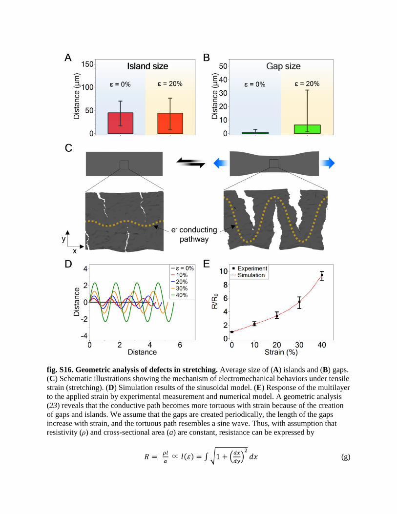
fig. S16. Geometric analysis of defects in stretching. Average size of (A) islands and (B) gaps.
(C) Schematic illustrations showing the mechanism of electromechanical behaviors under tensile
strain (stretching). (D) Simulation results of the sinusoidal model. (E) Response of the multilayer
to the applied strain by experimental measurement and numerical model. A geometric analysis
(23) reveals that the conductive path becomes more tortuous with strain because of the creation
of gaps and islands. We assume that the gaps are created periodically, the length of the gaps
increase with strain, and the tortuous path resembles a sine wave. Thus, with assumption that
resistivity (ρ) and cross-sectional area (a) are constant, resistance can be expressed by
𝑅 = 𝜌𝑙
𝑎 ∝ 𝑙(𝜀) = ∫√1 + (
𝑑𝑥
𝑑𝑦)2
𝑑𝑥 (g)
𝑦 = 𝐴 sin(𝐵𝑥) (h)
where ε is strain; x is variable; A is an amplitude which is a function of strain, f(ε); and B is a
function of strain, f(ε) = 2π/(1+ε).
The amplitude and a period should increase with strain. A can be determined by fitting to
experimental data (fig. S16D).
𝐴 = 49.7ε3 − 20.0ε2 + 5.8ε (i)
Thus, by knowing A, equation y is shown to increase with strain
𝑦 = 𝐴 sin(𝐵𝑥) = (49.7ε3 − 20.0ε2 + 5.8ε) sin((2𝜋
1+𝜀)𝑥) (j)
Because equation (g) does not have an analytical solution, it should be solved numerically. The
numerical solution of l and relative resistance are below
𝑙 = 𝑙𝑜1.1032 exp(5.4223𝜀) (k)
𝑅
𝑅𝑜=
𝑙
𝑙𝑜= 1.1032 exp(5.4223𝜀) (l)
where lo is the initial length of film, and Ro is an initial resistance. The excellent agreement
between the model and experiment (fig. S16E) allows us to gauge the resistance dependence on
strain.
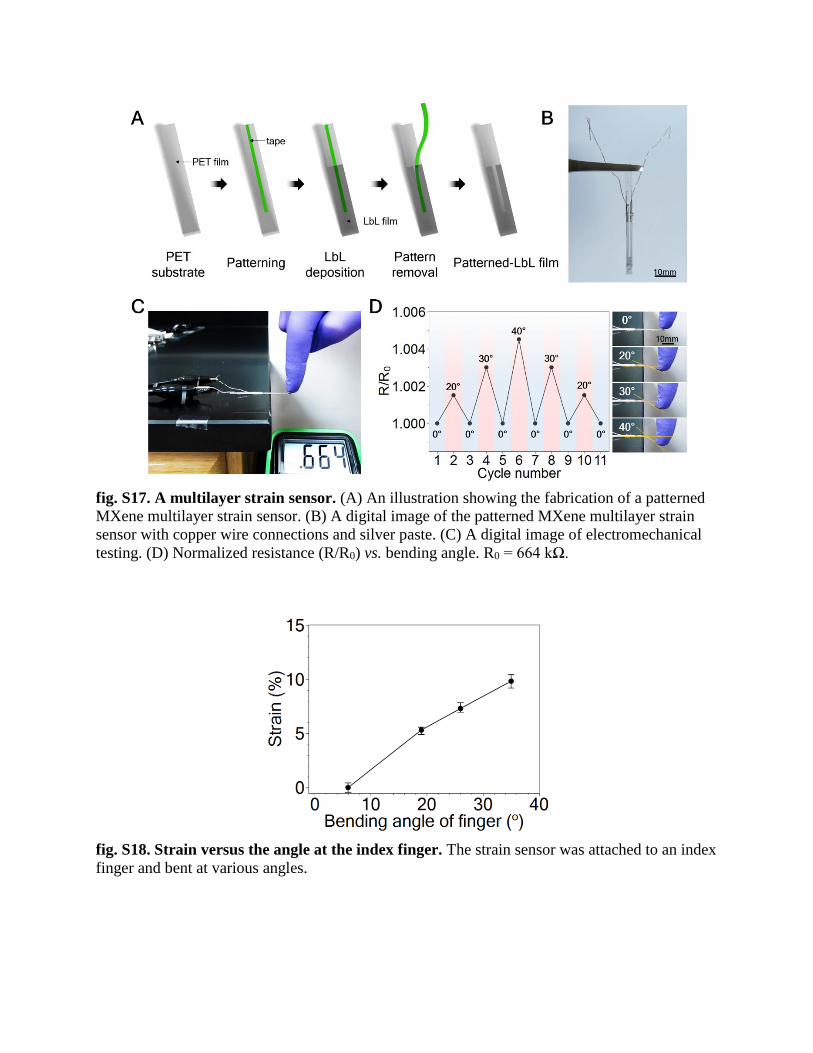
fig. S17. A multilayer strain sensor. (A) An illustration showing the fabrication of a patterned
MXene multilayer strain sensor. (B) A digital image of the patterned MXene multilayer strain
sensor with copper wire connections and silver paste. (C) A digital image of electromechanical
testing. (D) Normalized resistance (R/R0) vs. bending angle. R0 = 664 kΩ.
fig. S18. Strain versus the angle at the index finger. The strain sensor was attached to an index
finger and bent at various angles.
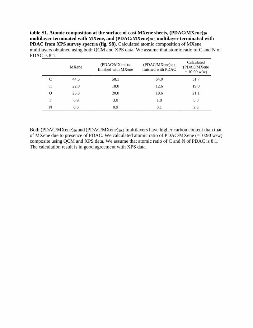
table S1. Atomic composition at the surface of cast MXene sheets, (PDAC/MXene)20
multilayer terminated with MXene, and (PDAC/MXene)20.5 multilayer terminated with
PDAC from XPS survey spectra (fig. S8). Calculated atomic composition of MXene
multilayers obtained using both QCM and XPS data. We assume that atomic ratio of C and N of
PDAC is 8:1.
MXene
(PDAC/MXene)20
finished with MXene
(PDAC/MXene)20.5
finished with PDAC
Calculated
(PDAC/MXene
= 10:90 w/w)
C 44.5 58.1 64.0 51.7
Ti 22.8 18.0 12.6 19.0
O 25.3 20.0 18.6 21.1
F 6.9 3.0 1.8 5.8
N 0.6 0.9 3.1 2.3
Both (PDAC/MXene)20 and (PDAC/MXene)20.5 multilayers have higher carbon content than that
of MXene due to presence of PDAC. We calculated atomic ratio of PDAC/MXene (=10:90 w/w)
composite using QCM and XPS data. We assume that atomic ratio of C and N of PDAC is 8:1.
The calculation result is in good agreement with XPS data.
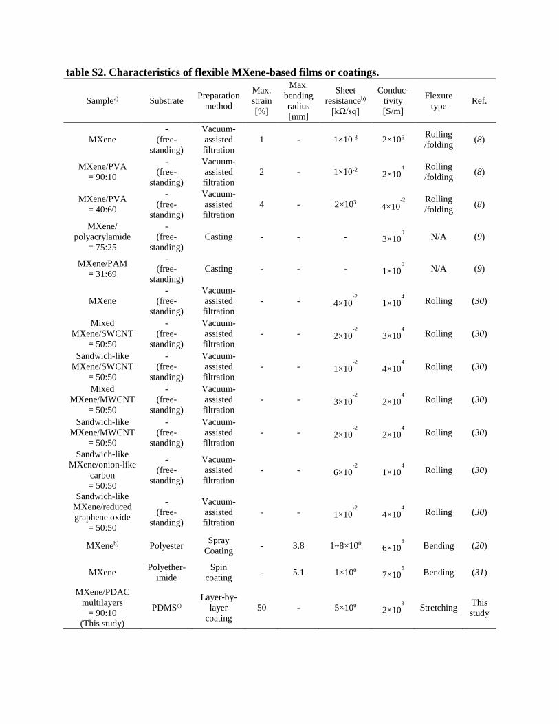
table S2. Characteristics of flexible MXene-based films or coatings.
Samplea) Substrate Preparation
method
Max.
strain
[%]
Max.
bending
radius
[mm]
Sheet
resistanceb)
[kΩ/sq]
Conduc-
tivity
[S/m]
Flexure
type Ref.
MXene
-
(free-
standing)
Vacuum-
assisted
filtration
1 - 1×10⁻³ 2×10⁵ Rolling
/folding (8)
MXene/PVA
= 90:10
-
(free-
standing)
Vacuum-
assisted
filtration
2 - 1×10⁻² 2×10⁴
Rolling
/folding (8)
MXene/PVA
= 40:60
-
(free-
standing)
Vacuum-
assisted
filtration
4 - 2×10³ 4×10⁻²
Rolling
/folding (8)
MXene/
polyacrylamide
= 75:25
-
(free-
standing)
Casting - - - 3×100
N/A (9)
MXene/PAM
= 31:69
-
(free-
standing)
Casting - - - 1×100
N/A (9)
MXene
-
(free-
standing)
Vacuum-
assisted
filtration
- - 4×10⁻²
1×10⁴
Rolling (30)
Mixed
MXene/SWCNT
= 50:50
-
(free-
standing)
Vacuum-
assisted
filtration
- - 2×10⁻²
3×10⁴
Rolling (30)
Sandwich-like
MXene/SWCNT
= 50:50
-
(free-
standing)
Vacuum-
assisted
filtration
- - 1×10⁻²
4×10⁴
Rolling (30)
Mixed
MXene/MWCNT
= 50:50
-
(free-
standing)
Vacuum-
assisted
filtration
- - 3×10⁻²
2×10⁴
Rolling (30)
Sandwich-like
MXene/MWCNT
= 50:50
-
(free-
standing)
Vacuum-
assisted
filtration
- - 2×10⁻²
2×10⁴
Rolling (30)
Sandwich-like
MXene/onion-like
carbon
= 50:50
-
(free-
standing)
Vacuum-
assisted
filtration
- - 6×10⁻²
1×10⁴
Rolling (30)
Sandwich-like
MXene/reduced
graphene oxide
= 50:50
-
(free-
standing)
Vacuum-
assisted
filtration
- - 1×10⁻²
4×10⁴
Rolling (30)
MXeneb) Polyester Spray
Coating - 3.8 1~8×100 6×10
3
Bending (20)
MXene Polyether-
imide
Spin
coating - 5.1 1×100 7×10
5
Bending (31)
MXene/PDAC
multilayers
= 90:10
(This study)
PDMSc)
Layer-by-
layer
coating
50 - 5×100 2×10³
Stretching This
study

MXene/PDAC
multilayers
= 90:10
(This study)
PETd)
Layer-by-
layer
coating
- 2.5 5×100 2×10³
Bending This
study
a)Based on weight ratio; b)Sheet resistance was calculated using Sheet resisatance [ohm sq-1] = 1/(conductivity [S m-
1] × thickness [m]) where sq is unitless; c)Polyethylene terephthalate; and d)Polydimethylsiloxane.
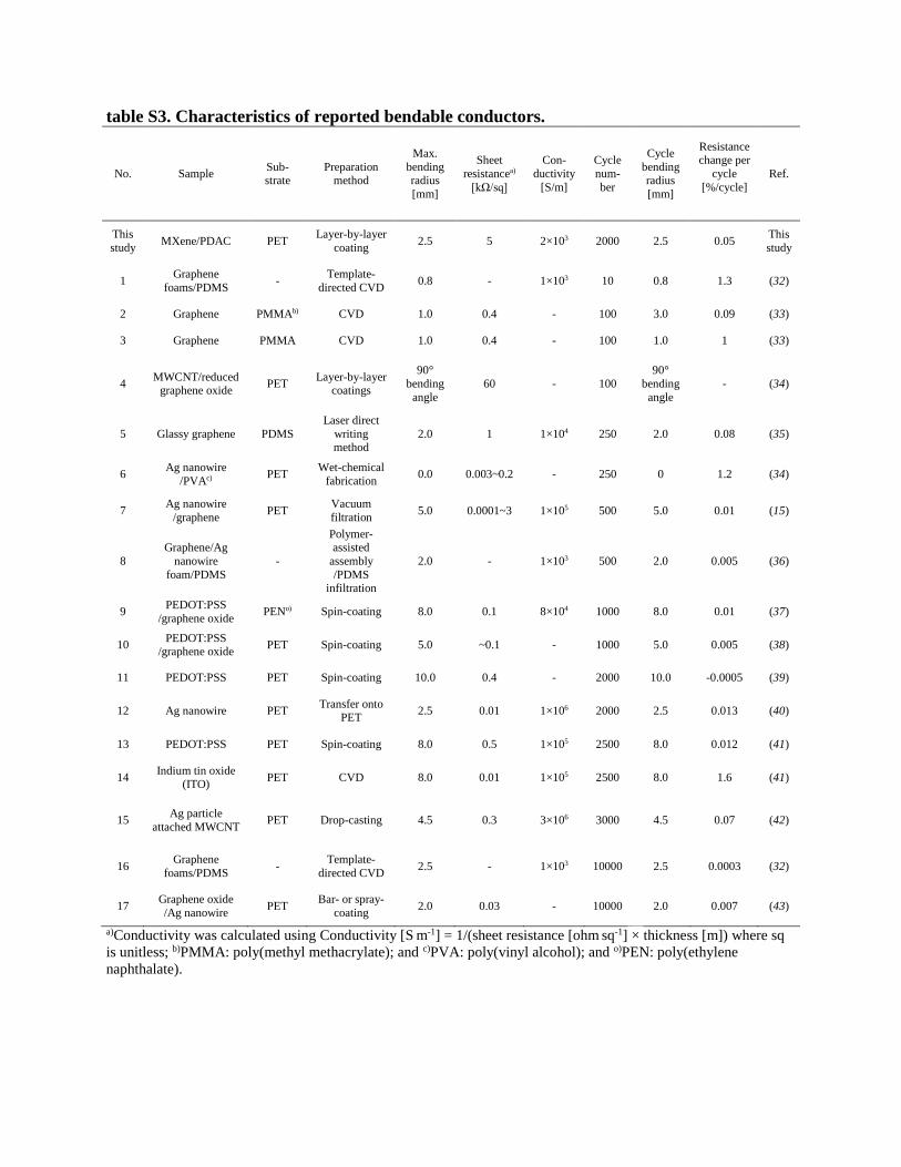
table S3. Characteristics of reported bendable conductors.
No. Sample Sub-strate
Preparation method
Max.
bending radius
[mm]
Sheet
resistancea)
[kΩ/sq]
Con-
ductivity
[S/m]
Cycle
num-
ber
Cycle
bending radius
[mm]
Resistance change per
cycle
[%/cycle]
Ref.
This
study MXene/PDAC PET
Layer-by-layer
coating 2.5 5 2×10³ 2000 2.5 0.05
This
study
1 Graphene
foams/PDMS -
Template-
directed CVD 0.8 - 1×10³ 10 0.8 1.3 (32)
2 Graphene PMMAb) CVD 1.0 0.4 - 100 3.0 0.09 (33)
3 Graphene PMMA CVD 1.0 0.4 - 100 1.0 1 (33)
4 MWCNT/reduced
graphene oxide PET
Layer-by-layer coatings
90°
bending
angle
60 - 100
90°
bending
angle
- (34)
5 Glassy graphene PDMS
Laser direct
writing method
2.0 1 1×10⁴ 250 2.0 0.08 (35)
6 Ag nanowire
/PVAc) PET
Wet-chemical
fabrication 0.0 0.003~0.2 - 250 0 1.2 (34)
7 Ag nanowire
/graphene PET
Vacuum
filtration 5.0 0.0001~3 1×10⁵ 500 5.0 0.01 (15)
8
Graphene/Ag
nanowire
foam/PDMS
-
Polymer-assisted
assembly
/PDMS infiltration
2.0 - 1×10³ 500 2.0 0.005 (36)
9 PEDOT:PSS
/graphene oxide PENo) Spin-coating 8.0 0.1 8×10⁴ 1000 8.0 0.01 (37)
10 PEDOT:PSS
/graphene oxide PET Spin-coating 5.0 ~0.1 - 1000 5.0 0.005 (38)
11 PEDOT:PSS PET Spin-coating 10.0 0.4 - 2000 10.0 -0.0005 (39)
12 Ag nanowire PET Transfer onto
PET 2.5 0.01 1×10⁶ 2000 2.5 0.013 (40)
13 PEDOT:PSS PET Spin-coating 8.0 0.5 1×10⁵ 2500 8.0 0.012 (41)
14 Indium tin oxide
(ITO) PET CVD 8.0 0.01 1×10⁵ 2500 8.0 1.6 (41)
15 Ag particle
attached MWCNT PET Drop-casting 4.5 0.3 3×10⁶ 3000 4.5 0.07 (42)
16 Graphene
foams/PDMS -
Template-
directed CVD 2.5 - 1×10³ 10000 2.5 0.0003 (32)
17 Graphene oxide
/Ag nanowire PET
Bar- or spray-
coating 2.0 0.03 - 10000 2.0 0.007 (43)
a)Conductivity was calculated using Conductivity [S m-1] = 1/(sheet resistance [ohm sq-1] × thickness [m]) where sq
is unitless; b)PMMA: poly(methyl methacrylate); and c)PVA: poly(vinyl alcohol); and o)PEN: poly(ethylene
naphthalate).
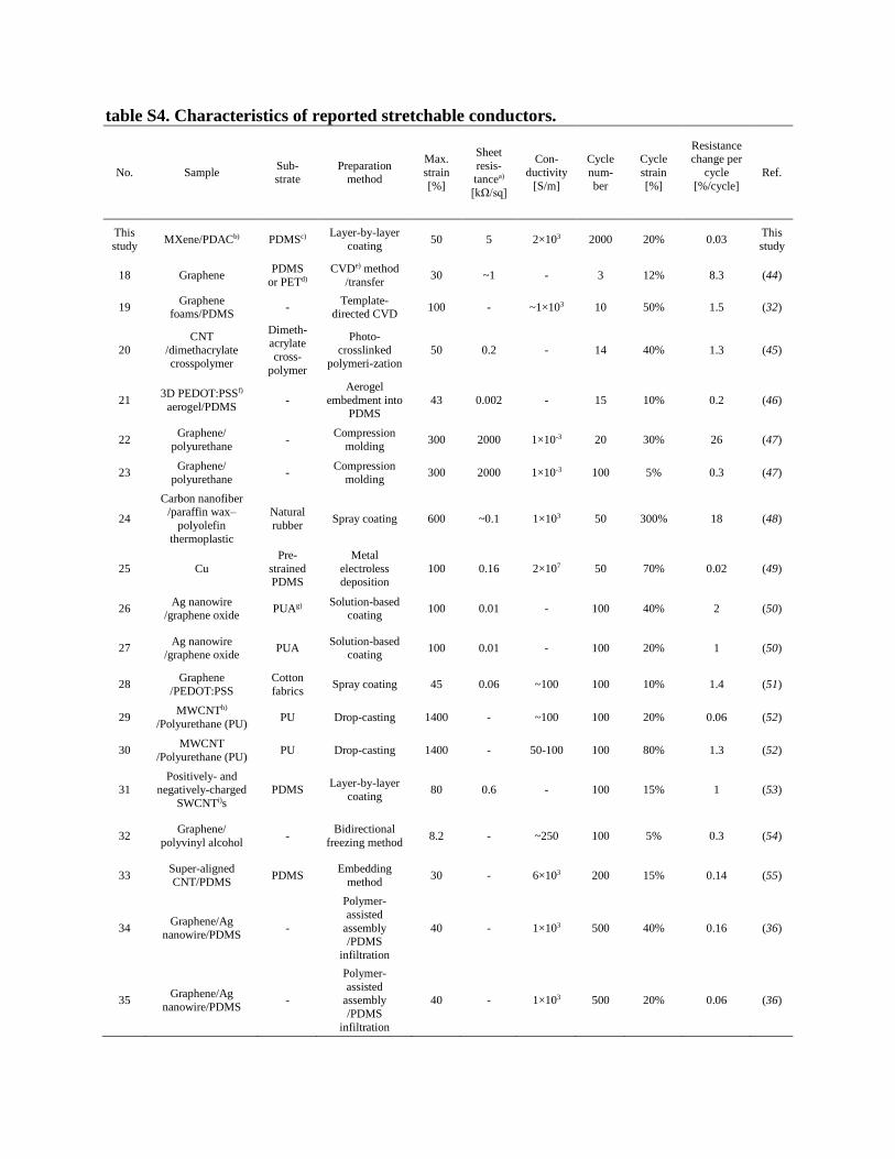
table S4. Characteristics of reported stretchable conductors.
No. Sample Sub-strate
Preparation method
Max.
strain
[%]
Sheet
resis-tancea)
[kΩ/sq]
Con-
ductivity
[S/m]
Cycle
num-
ber
Cycle
strain
[%]
Resistance change per
cycle
[%/cycle]
Ref.
This
study MXene/PDACb) PDMSc)
Layer-by-layer
coating 50 5 2×10³ 2000 20% 0.03
This
study
18 Graphene PDMS
or PETd)
CVDe) method
/transfer 30 ~1 - 3 12% 8.3 (44)
19 Graphene
foams/PDMS -
Template-directed CVD
100 - ~1×10³ 10 50% 1.5 (32)
20
CNT
/dimethacrylate
crosspolymer
Dimeth-acrylate
cross-
polymer
Photo-
crosslinked
polymeri-zation
50 0.2 - 14 40% 1.3 (45)
21 3D PEDOT:PSSf)
aerogel/PDMS -
Aerogel
embedment into PDMS
43 0.002 - 15 10% 0.2 (46)
22 Graphene/
polyurethane -
Compression
molding 300 2000 1×10⁻³ 20 30% 26 (47)
23 Graphene/
polyurethane -
Compression
molding 300 2000 1×10⁻³ 100 5% 0.3 (47)
24
Carbon nanofiber /paraffin wax–
polyolefin
thermoplastic
Natural
rubber Spray coating 600 ~0.1 1×10³ 50 300% 18 (48)
25 Cu
Pre-
strained PDMS
Metal
electroless deposition
100 0.16 2×10⁷ 50 70% 0.02 (49)
26 Ag nanowire
/graphene oxide PUAg)
Solution-based coating
100 0.01 - 100 40% 2 (50)
27 Ag nanowire
/graphene oxide PUA
Solution-based coating
100 0.01 - 100 20% 1 (50)
28 Graphene
/PEDOT:PSS
Cotton
fabrics Spray coating 45 0.06 ~100 100 10% 1.4 (51)
29 MWCNTh)
/Polyurethane (PU) PU Drop-casting 1400 - ~100 100 20% 0.06 (52)
30 MWCNT
/Polyurethane (PU) PU Drop-casting 1400 - 50-100 100 80% 1.3 (52)
31 Positively- and
negatively-charged
SWCNTi)s
PDMS Layer-by-layer
coating 80 0.6 - 100 15% 1 (53)
32 Graphene/
polyvinyl alcohol -
Bidirectional
freezing method 8.2 - ~250 100 5% 0.3 (54)
33 Super-aligned
CNT/PDMS PDMS
Embedding
method 30 - 6×10³ 200 15% 0.14 (55)
34 Graphene/Ag
nanowire/PDMS -
Polymer-
assisted
assembly /PDMS
infiltration
40 - 1×10³ 500 40% 0.16 (36)
35 Graphene/Ag
nanowire/PDMS -
Polymer-
assisted assembly
/PDMS
infiltration
40 - 1×10³ 500 20% 0.06 (36)
36 Graphene/natural
rubber
natural
rubber
Solution-based
coating ~800 - ~0.1 920 75% -0.08 (56)
37 Graphene /graphene
scrolls SEBSj) CVD 100 0.1 - 1000 90% 0.8 (57)
38 SWCNT PUAk) Drop-casting 50 0.02 - 1000 20% 0.06 (58)
39 Super-aligned CNT PDMS Transfer onto
PDMS 600 - - 5000 400% 0.0012 (59)
40 Ag/MWCNT NBR Drop-casting 140 - 6×10⁵ 5000 20% 0.02 (60)
41
SWCNT
/fluorinated copolymer
PDMS Drop-casting 134 - 6×10³ 10000 50% 0.007 (1)
42 Au nanoparticle
/PU -
Layer-by-layer coating
16 - 7×10⁵ 10000 5% -0.004 (12)
43 Au nanoparticle
/PU -
Vacuum assisted
filtration 75 - 5×10⁴ 10000 5% -0.003 (12)
44 F4TCNQl)-doped
SWCNT PDMS
Spray-coating
and buckling 150 0.3 1×10⁵ 12500 25% 0 (61)
a)Conductivity was calculated using Conductivity [S m-1] = 1/(sheet resistance [ohm sq-1] × thickness [m]) where sq
is unitless; b)PDAC: poly(diallyldimethylammonium chloride); c)PDMS: poly(dimethylsiloxane); d)PET:
poly(ethylene terephthalate); e)CVD: chemical vapor deposition; f)PEDOT:PSS: poly(3,4-
ethylenedioxythiophene):polystyrene sulfonate; g)PUA: polyurethane acrylate; h)MWCNT: multi-walled carbon
nanotubes; i)SWCNT: single-walled carbon nanotubes; j)SEBS: styrene-ethylene-butadiene-styrene; k)NBR: nitrile
butadiene rubber; and l)F4TCNQ: 2,3,5,6-tetrafluoro-7,7,8,8-tetracyanoquinodimethane.
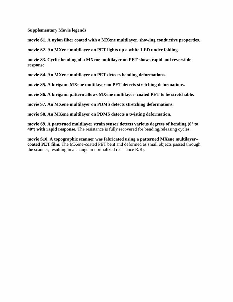
Supplementary Movie legends
movie S1. A nylon fiber coated with a MXene multilayer, showing conductive properties.
movie S2. An MXene multilayer on PET lights up a white LED under folding.
movie S3. Cyclic bending of a MXene multilayer on PET shows rapid and reversible
response.
movie S4. An MXene multilayer on PET detects bending deformations.
movie S5. A kirigami MXene multilayer on PET detects stretching deformations.
movie S6. A kirigami pattern allows MXene multilayer–coated PET to be stretchable.
movie S7. An MXene multilayer on PDMS detects stretching deformations.
movie S8. An MXene multilayer on PDMS detects a twisting deformation.
movie S9. A patterned multilayer strain sensor detects various degrees of bending (0° to
40°) with rapid response. The resistance is fully recovered for bending/releasing cycles.
movie S10. A topographic scanner was fabricated using a patterned MXene multilayer–
coated PET film. The MXene-coated PET bent and deformed as small objects passed through
the scanner, resulting in a change in normalized resistance R/R0.
![Gilbert damping in binary magnetic multilayers · E. BARATI AND M. CINAL PHYSICAL REVIEW B 95, 134440 (2017) ons-d exchangeattheinterfaces,hasbeenproposedbyBerger [53]. More recently,](https://static.fdocument.org/doc/165x107/5d4e675988c99303708b99e1/gilbert-damping-in-binary-magnetic-multilayers-e-barati-and-m-cinal-physical.jpg)