The inner structure of haloes in Cold+Warm dark matter models
Wis
sens
chaf
tlich
-Tec
hnis
che
Beric
hte
FZD
-470
200
7 · I
SSN
143
7-32
2X
FZD-470
STRUCTURE OF MATTER
TRIENNIAL SCIENTIFIC REPORT 2004 -2007 I Volume 1
1
PREFACE
FOCUS
FACILITIES FOR EUROPE
Center for Application of Ion Beams to Materials Research (AIM)
The Dresden High Magnetic Field Laboratory (HLD)
The Radiation Source ELBE
Materials research with synchrotron radiation at ROBL
RESEARCH
Hadron mass: Why so heavy?
ELBE γ-rays shed light on the origin of the chemical elements
nELBE: Novel research on transmutation of radioactive waste
Quantum phase transitions in an exotic metal
Searching for the magnetic Bose-Einstein condensate
Ions meet magnets – tailor-made properties on the nano-scale
Cubic boron nitride: Thin film physics moving toward a practical application
Ion-beam synthesis of nanostructures for micro- and nanoelectronics
Silicon-based light emitters – from infrared to ultraviolet
Ultrafast infrared spectroscopy of semiconductor quantum structures
FACTS & FIGURES
2
4
6
8
10
12
14
17
20
23
25
27
30
32
34
37
40
Content
Cover picture: 3D scheme of an ion beam hitting the surface of a solid material (picture: Sander Münster)Photo left: Sven Claus
2
Preface
This volume of the Triennial Scientific Report highlights the scientific output of the FZDresearch program “Structure of Matter”, covering the years 2004 to 2007. It is the firstout of three volumes that are published this year for the first time. In future, we plan tosubstitute our present Annual Report about all the research activities at the Forschungs-zentrum by Biannual Reports. These will be dedicated to the three research programs“Structure of Matter”, “Environment and Safety”, and “Life Sciences”, respectively. Theywill provide the scientists of the FZD with the opportunity to present their research resultsto their colleagues, but also to a wider audience interested in sciences.
The first part of this Triennial Report introduces the “Structure of Matter” program aswell as the large-scale facilities that are used for research within this program. The secondpart consists of ten articles on research projects that were conducted by scientists of theInstitute of Radiation Physics, the Institute Dresden High Magnetic Field Laboratory, andthe Institute of Ion-Beam Physics and Materials Research.
This report is primarily concerned with science. Nevertheless, we also want to take theopportunity and inform you about news from the FZD. During the last 18 months newprograms for young and international scientists have been developed and someorganizational changes occurred. In 2006, we launched the first Ph.D. seminar at the FZDwith about 100 participants. As this seminar was a big success, the second Ph.D. seminarfollowed soon in September 2007. An outcome of these seminars was a series of FZDlectures that started at the beginning of 2007 and will continue on a regular basisthroughout 2007 and 2008. Furthermore, special workshops have been offered to youngscientists, e.g. communication to the media, presentation in English, training for youngscience managers, etc. Talented postdoctoral staff can benefit from a newly installedtenure track program that gives them financial freedom to lead a group of youngscientists and full responsibility for the scientific success of the group. The FZD fellowsprogram aims at working more closely together with highly renowned internationalcooperation partners who are invited for special research projects at the FZD.
The last 18 months were also characterized by an intense discussion about the future ofthe FZD. In meetings and seminars we debated about the status and the future of theForschungszentrum Dresden-Rossendorf, asking questions like: “What are our futurescientific objectives?” “Which research methods and facilities are required in order toreach those goals?” “How can new research activities be funded and who are our futurecooperation partners?”
To successfully compete with other research institutions worldwide, it is important toparticipate in networks. On the one hand, these can be networks within the researchcenter and, on the other hand, networks on the national and international level. Forenhancing the interdisciplinary cooperation between the FZD institutes, the large-scalefacilities have provided a strong unifying moment. To give one example: the RadiationSource ELBE is used for materials research and nuclear physics as well as for biophysical,medical, or radiochemical experiments. It is thus employed by all six institutes of the FZD.
Roland Sauerbrey I Scientific Director
PREFACE
3
Prof. Dr. Roland Sauerbrey
Furthermore, ELBE offers an excellent research platform for external users, which is mainlydue to the two free-electron lasers that are operated as a user facility. The UniversitätHalle-Wittenberg is in charge of the positron beam-line whereas scientists from theTechnische Universität Dresden generate neutrons for nuclear physics experiments andresearch on the transmutation of radioactive waste. In a special workshop, dedicated tothe Radiation Source ELBE, in-house and external users together with scientists fromleading accelerator laboratories discussed future prospects and tasks of the ELBE facility.
The Dresden High Magnetic Field Laboratory, which is a common project of five Dresdenmaterials research institutions, welcomed its first user groups in 2007. As a member of aEuropean network this laboratory provides a unique environment for measuring solid-state materials in high magnetic fields. Magnetism is also the focus of the “NanoscaleMagnetism” group employing the analytical methods of the High Field Laboratory, butalso making use of ion-beam techniques at the Ion-Beam Center in Rossendorf. Here, thenew research field “Nano-Spintronics” under the direction of Dr. Heidemarie Schmidt wasestablished in 2007. This group of five scientists is especially interested in experimentswith the Focussed Ion Beam—a perfect tool for producing nano-structures beneath thesurface of almost any material— which can thus be applied to the fabrication of magneticsemiconductors.
A high-intensity laser laboratory is currently under construction and will be put intooperation in the beginning of 2008. The Laser-Particle Acceleration Group was founded in November 2006 and comprises six scientists and laser engineers now. Besides basicresearch on the interaction of particles with matter their main goal is to generate newparticle radiation for radiation therapy in the future war against cancer. In the veryexciting new project “onCOOPtics”, funded by the German Federal Ministry of Educationand Research (BMBF), with laser physicists from Jena, medical doctors from the UniversityHospital Dresden, and scientists from the FZD we hope to explore the fundamentals for anew laser tool that can be applied for tumor research as well as for effective radiationtherapy in ten to fifteen years. More information about this new research project is givenin the third volume of the Triennial Scientific Report focusing on “Life Sciences”.
Finally, I would like to thank our partners in both the state and the federal governmentfor their continued support, our national and international scientific cooperation partnersfor many successful joint research endeavors and, last but not least, the entire staff of theFZD for their dedicated work for this fine institution.
4
Structure of Matter program at the Forschungszentrum Dresden-Rossendorf
5
Wolfhard Möller, Manfred Helm, Joachim Wosnitza, Burkhard Kämpfer
The FZD research platform consists of the Structure of Matter program, the Life Sciencesprogram, and the Environment and Safety program. The activities of the Structure ofMatter program are centered on the response of matter to extreme irradiation conditionsand to strong electric and magnetic fields. Within the program areas of MaterialsResearch with Ions and Semiconductor Physics, fast ions and thin-film depositiontechniques are employed for the development of new materials with a prominent focuson nanosystems. In these program areas, novel structural and functional properties areinvestigated using a variety of macroscopic to nanoscopic diagnostics. Research with HighMagnetic Fields is concerned with the electronic properties of solid matter using ultrahightransient magnetic fields. The Subatomic Physics program studies rare hadronic processesin matter and nuclear processes which are relevant to nuclear technology andastrophysics.
For these topics, the infrastructure at FZD offers four large-scale experimental facilities.The Ion-Beam Center houses ion-beam and plasma devices that deliver ions at energiesbetween approximately 10 eV and 5 MeV for surface modification and analysis, as well as for thin-film deposition. Ion beams are used to create high-performance materials withspecific and often nanostructure-based functions for electronic, optical, and magnetic applications. In addition to the in-house research activities, the Ion-Beam Center serves as a national and international user facility for research and industry, and is funded withinthe European Commission’s Transnational Access.
The Rossendorf Beamline, located at the European Synchrotron Radiation Facility (ESRF)in Grenoble, contributes fundamentally to materials research at the FZD, offering X-raydiffraction and reflection, particularly in several real-time in-situ devices for thermal treatment and thin-film deposition.
The Radiation Source ELBE features numerous particle and photon beams. Its electronbeam is applied both directly and through the production of high-energy photons, neutrons, and positrons. Two attached free-electron lasers deliver high-intensity coherentinfrared light. They are also funded by the European Commission and providetransnational access to external users. The free-electron lasers’ mid- and far-infraredradiation is well suited to studying semiconductor materials.
The Dresden High Magnetic Field Laboratory has set an ambitious goal to provide 100 Tesla in millisecond pulses for materials research in order to study the electronicproperties of materials such as high-temperature superconductors, magnets, orsemiconductors, even in combination with the ELBE free-electron lasers.
A High-Intensity Laser Laboratory is currently under construction. Laser-accelerated ionswill be used there for multidisciplinary studies of non-linear particle-matter interaction. This topic underscores the goal of the FZD of increasingly interlinking the activities of its three programs. Biological templating of metallic nanostructures, physico-chemicalcharacterization of radionuclide complexes, measurement of transmutation cross-sections,and tomographic characterization of pulsed magnet coils are additional examples ofinternal interdisciplinary cooperation with the Life Sciences and Environment and Safetyprogram. The research activities of all three programs are also connected by the use ofELBE and the diagnostic facilities belonging to the Ion-Beam Center and the RossendorfBeamline at ESRF.
FOCUS
6
Andreas Kolitsch, Wolfhard Möller
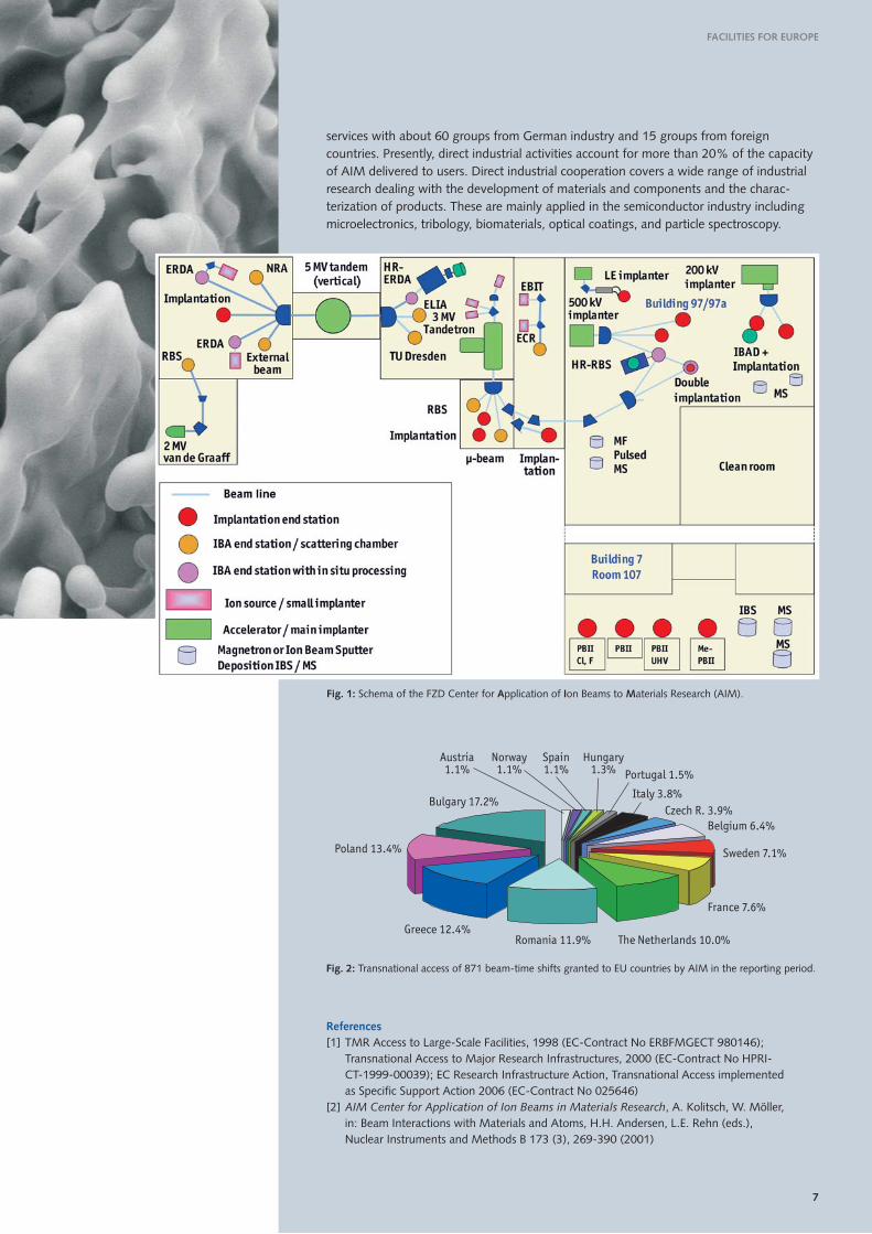
The Center for Application of Ion Beams toMaterials Research (AIM) is devoted to theapplication of ion beams to modify andanalyze near-surface layers of materials.The ion-beam center (Fig. 1) operatesthree MV electrostatic accelerators, threeion implanters, a fine-focused ion-beamdevice, a highly-charged ion device, andseveral experimental installations forplasma immersion implantation as well asion-assisted deposition of thin films. Thisbroad spectrum of ion-beam equipment isavailable in the energy range from severaleV up to several MeV. The main sectionsof the facility have been installed withinthe last 12 years and represent world-classquality.
The aim of the research activities at AIM isto contribute to the development ofEuropean materials research by using thediverse possibilities of ion-beamtechniques. Basic research to explore newpossibilities for surface modification ofmaterials by ion irradiation is combinedwith the development of technologicalapplications in cooperation with industry.
More than 40% of user time of AIMdevices is made available to external usersfrom universities and other researchinstitutions. About 60 research projectsfrom Germany, stemming from roughly thesame number of research groups benefitedfrom AIM facilities from January 2004 toDecember 2006. Moreover, 70 groupsfrom the rest of the EU and its associated
countries and 25 groups from otherforeign countries made use of AIM. Fig. 2demonstrates the widespread distributionof access in EU countries during thisperiod. External users have requested usefor almost all of the center’s experimentalfacilities. In addition, a broad spectrum ofresearch topics not only in materialsscience, but also in the life sciences, arts,archeology, and geology are covered aswell.
During the past several years, AIM hascontinuously expanded its industrialcooperation projects and services. Industryplays a major role through partnerships incooperative projects utilizing in-houseresearch. From 2004 to 2006, there weredirect cooperation projects and industrial
Center for Application of Ion Beams to Materials Research (AIM)
Facilities for Europe
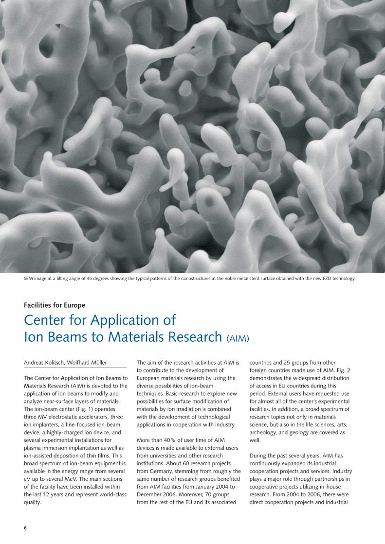
SEM image at a tilting angle of 45 degrees showing the typical patterns of the nanostructures at the noble metal stent surface obtained with the new FZD technology.
FACILITIES FOR EUROPE
7
services with about 60 groups from German industry and 15 groups from foreigncountries. Presently, direct industrial activities account for more than 20% of the capacityof AIM delivered to users. Direct industrial cooperation covers a wide range of industrialresearch dealing with the development of materials and components and the charac-terization of products. These are mainly applied in the semiconductor industry includingmicroelectronics, tribology, biomaterials, optical coatings, and particle spectroscopy.
Fig. 1: Schema of the FZD Center for Application of Ion Beams to Materials Research (AIM).
Fig. 2: Transnational access of 871 beam-time shifts granted to EU countries by AIM in the reporting period.
References[1] TMR Access to Large-Scale Facilities, 1998 (EC-Contract No ERBFMGECT 980146);
Transnational Access to Major Research Infrastructures, 2000 (EC-Contract No HPRI-CT-1999-00039); EC Research Infrastructure Action, Transnational Access implemented as Specific Support Action 2006 (EC-Contract No 025646)
[2] AIM Center for Application of Ion Beams in Materials Research, A. Kolitsch, W. Möller, in: Beam Interactions with Materials and Atoms, H.H. Andersen, L.E. Rehn (eds.), Nuclear Instruments and Methods B 173 (3), 269-390 (2001)
8
Joachim Wosnitza
High magnetic fields are one of the mostpowerful tools available to scientists for thestudy, modification, and control of thestate of matter. This is fundamentally dueto the unique property of the magneticfield to act universally on the charge andthe spin of particles. In other words, itconstitutes one of the few fundamentalthermodynamic parameters (liketemperature) which change the state ofmatter in a controlled way. Magnetic fieldsare particularly interesting since theinduced changes are, almost withoutexception, reversible as static magneticfields do not add kinetic energy to thesystem. Since these spin and orbitaldegrees of freedom control most of the
electronic and magnetic properties ofmatter, it is natural to use the magneticfield to investigate and modify them. Ingeneral, the higher the field, the moreclearly the field-induced changes can beobserved and the more transitions to newfundamental states of matter becomevisible. Consequently, there is a growingdemand for higher and higher magneticfields in combination with a reliable andsophisticated sample diagnostics.
In 2002 the German Science Counciltherefore strongly recommended fundingof the Hochfeld-Magnetlabor Dresden(HLD) at the FZD. The proposal for thispulsed-field facility was based on acollaborative initiative of five Dresdeninstitutions. The construction of the
Joachim Wosnitza in the capacitor bank hall of the HLD.
The Dresden High Magnetic Field Laboratory (HLD)
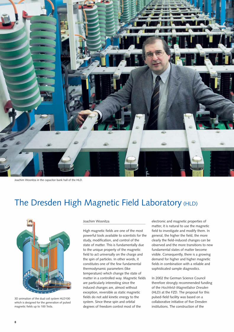
3D animation of the dual coil system HLD100which is designed for the generation of pulsedmagnetic fields up to 100 Tesla.
FACILITIES FOR EUROPE
9
Photo: W.H. Schmidt
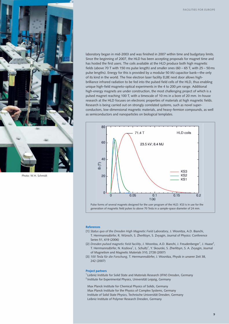
laboratory began in mid-2003 and was finished in 2007 within time and budgetary limits.Since the beginning of 2007, the HLD has been accepting proposals for magnet time andhas hosted the first users. The coils available at the HLD produce both high magneticfields (above 70 T with 150 ms pulse length) and smaller ones (60 – 65 T, with 25 – 50 mspulse lengths). Energy for this is provided by a modular 50 MJ capacitor bank—the onlyof its kind in the world. The free electron laser facility ELBE next door allows high-brilliance infrared radiation to be fed into the pulsed field cells of the HLD, thus enablingunique high-field magneto-optical experiments in the 4 to 200 µm range. Additionalhigh-energy magnets are under construction, the most challenging project of which is apulsed magnet reaching 100 T, with a timescale of 10 ms in a bore of 20 mm. In-houseresearch at the HLD focuses on electronic properties of materials at high magnetic fields.Research is being carried out on strongly correlated systems, such as novel super-conductors, low-dimensional magnetic materials, and heavy-fermion compounds, as wellas semiconductors and nanoparticles on biological templates.
References[1] Status quo of the Dresden High Magnetic Field Laboratory, J. Wosnitza, A.D. Bianchi,
T. Herrmannsdörfer, R. Wünsch, S. Zherlitsyn, S. Zvyagin, Journal of Physics: Conference Series 51, 619 (2006)
[2] Dresden pulsed magnetic field facility, J. Wosnitza, A.D. Bianchi, J. Freudenberger1, J. Haase2,T. Herrmannsdörfer, N. Kozlova1, L. Schultz1, Y. Skourski, S. Zherlitsyn, S. A. Zvyagin, Journal of Magnetism and Magnetic Materials 310, 2728 (2007)
[3] 100 Tesla für die Forschung, T. Herrmannsdörfer, J. Wosnitza, Physik in unserer Zeit 38, 242 (2007)
Project partners1 Leibniz Institute for Solid State and Materials Research (IFW) Dresden, Germany2 Institute for Experimental Physics, Universität Leipzig, Germany
Max Planck Institute for Chemical Physics of Solids, GermanyMax Planck Institute for the Physics of Complex Systems, GermanyInstitute of Solid State Physics, Technische Universität Dresden, GermanyLeibniz Institute of Polymer Research Dresden, Germany
Pulse forms of several magnets designed for the user program of the HLD. KS3 is in use for thegeneration of magnetic field pulses to above 70 Tesla in a sample-space diameter of 24 mm.
10
Peter Michel, Burkhard Kämpfer
By studying the interaction of variousforms of radiation with matter in atomicand subatomic dimensions as well as withtissues, cells and their components, we cangain a wide range of new insights intotheir structures and functionalities. At theheart of ELBE (Electron Linear acceleratorwith high Brilliance and low Emittance) is a superconducting linear acceleratorconsisting of two units which are cooled byliquid helium. It delivers a quasi-continuouselectron beam of 5 to 40 MeV beamenergy at beam currents of up to 1 mA.This primary beam is characterized by anespecially low transverse emittance ofbetter than 10 mm mrad (even less than 2 mm mrad has been achieved at lowbunch charges) and short pulses (typically2 ps bunch length) with low energy spreadand flexible temporal structure.
Due to these unusual properties, a varietyof secondary radiation types are availablefor experiments:
(i) Two Free Electron Lasers (FELs) withundulators of 27 mm and 100 mm periodlength deliver coherent radiation in the midand far infrared. More precisely, thewavelength of the U27-FEL ranges from 4to 22 µm while U100-FEL covers the rangefrom 20 to 200 µm. Depending on thewavelength, several watts of optical powercan typically be coupled out. The infraredlight beams are transported to severaloptical laboratories, where a broad rangeof different experiments are conducted.The primary fields of research includesemiconductor physics (ground-statevibration-population decay or experimentsto determine the relaxation time ofelectrons in superlattices or self-assembledquantum dots), biophysics (IR-inducedchanges in thin DNA films), environmentaland safety research, as well as experimentsin ellipsometry and near-field microscopy.
Furthermore, an additional transfer systemdirects the FEL light into the Dresden HighMagnetic Field Laboratory (HLD) situatedin a nearby building.
(ii) The high primary-beam current allowsgeneration of intense secondary neutronbeams, either in reactions with a rotatingtungsten disc or a liquid-lead target. Theemerging neutron pulses carry the timestructure of the primary electron beam,making them well suited for time-of-flightexperiments. Given this, neutron-inducedreactions are used to complete thedatabase for fusion-reactor materials, fortransmutation of nuclear waste, and forcertain steps in the astrophysical breedingprocesses of chemical elements.
(iii) By pair production from the intensegamma radiation field, positrons areproduced in a stack of tungsten radiatorfoils. These will be extracted and deliveredas a secondary beam for investigations inmaterials science.
Free-Electron Laser at FZD. Photo: Sven Claus
The Radiation Source ELBE
FACILITIES FOR EUROPE
11
1: Diagnostic station, IR-imaging and biological IR experiment2: Femtosecond laser, THz-spectroscopy, IR pump-probe experiment3: Time-resolved semiconductor spectroscopy, THz-spectroscopy
4: FTIR, biological IR experiment5: Near-field and pump-probe IR experiment6: Radiochemistry and sum-frequency-generation experiment,
photothermal beam-deflection spectroscopy
(iv) The propagation of the well-collimatedprimary electron beam through crystals,such as diamonds, generates channellingradiation, i.e., X-rays in the 10 to 100 keVrange. These X-rays are used within theBiostructures and Radiation program toinvestigate cell damage due to irradiation.
(v) Irradiating a thin foil with the primaryelectron beam generates hard X-rays withenergies up to 20 MeV. By exposingselected isotopes to these X-rays, theirexcitation and transformation into otherisotopes through various reactions can bestudied. Understanding of what occurs incross-sections such as these is importantfor understanding and modelling thecooking of chemical elements in explosive-star phenomena. These investigationscomplement those in item (ii). Furtherdetails can be studied by exposing isotopesdirectly to the electron beam.
(vi) Due to the excellent time structure andhigh intensity of the primary ELBE beam,state-of-the-art detectors with excellenttime resolution (below 100 ps sigma) andsufficient stability in a high rate environ-ment – between 10.000 and 50.000charged particles impinging on the detector
per cm2 per second – are developed. Thesedetectors fulfil the challenging require-ments of new experiments at the futureFacility for Anti-proton and Ion Research(FAIR), and of modern applications inneutron, particle, and medical physics.
The electron-beam quality stronglydepends on the electron source (i.e., thegun). In the first years of the operation ofELBE, a thermionic gun was used. Researchand development of a unique supercon-ducting radio frequency gun is almostcompleted. It will be installed in 2007.
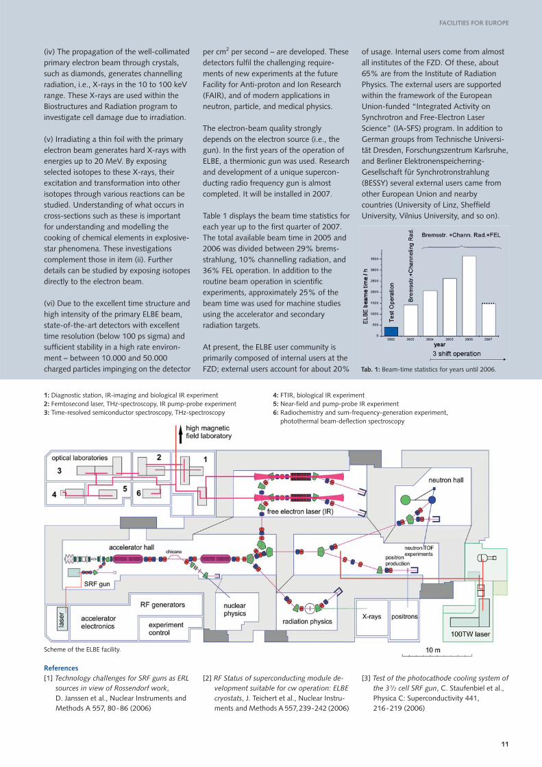
Table 1 displays the beam time statistics foreach year up to the first quarter of 2007.The total available beam time in 2005 and2006 was divided between 29% brems-strahlung, 10% channelling radiation, and36% FEL operation. In addition to theroutine beam operation in scientificexperiments, approximately 25% of thebeam time was used for machine studiesusing the accelerator and secondaryradiation targets.
At present, the ELBE user community isprimarily composed of internal users at theFZD; external users account for about 20%
of usage. Internal users come from almostall institutes of the FZD. Of these, about65% are from the Institute of RadiationPhysics. The external users are supportedwithin the framework of the EuropeanUnion-funded “Integrated Activity onSynchrotron and Free-Electron LaserScience” (IA-SFS) program. In addition toGerman groups from Technische Universi-tät Dresden, Forschungszentrum Karlsruhe,and Berliner Elektronenspeicherring-Gesellschaft für Synchrotronstrahlung(BESSY) several external users came fromother European Union and nearbycountries (University of Linz, SheffieldUniversity, Vilnius University, and so on).
Tab. 1: Beam-time statistics for years until 2006.
Scheme of the ELBE facility.
References[1] Technology challenges for SRF guns as ERL
sources in view of Rossendorf work, D. Janssen et al., Nuclear Instruments and Methods A 557, 80-86 (2006)
[2] RF Status of superconducting module de-velopment suitable for cw operation: ELBE cryostats, J. Teichert et al., Nuclear Instru-ments and Methods A 557,239-242 (2006)
[3] Test of the photocathode cooling system ofthe 31/2 cell SRF gun, C. Staufenbiel et al., Physica C: Superconductivity 441, 216-219 (2006)
12
Johannes von Borany, Carsten Bähtz, Jörg Grenzer
Synchrotron radiation is one of the mostversatile tools for structural diagnostics inmaterials science, as the X-ray wavelength(~ Å) matches perfectly with inter-atomicdistances. Detailed information concerningcrystalline phases, lattice parameters,particle (grain) sizes, texture, micro-stress,or surface and interface properties can bederived from X-ray scattering anddiffraction experiments. When combinedwith X-ray fluorescence and absorption
spectroscopy, the chemical compositionand local bonding properties becomeaccessible as well. Unlike transmissionelectron microscopy or probemeasurements with near-atomic spatialresolution, X-ray methods usually delivercharacteristic (“averaged”) data on largeareas, but X-ray micro-focus solutions alsoenable spatially resolved local informationon patterned or inhomogeneous materialsor microstructures. Depth profiling ispossible via energy or incidence/exit anglevariation.
The Rossendorf Beamline (ROBL),operated by FZD, is a bending magnetsynchrotron radiation user facility locatedat BM20 of the European SynchrotronRadiation Facility (ESRF) in Grenoble,France. In operation since 1998, it offerstwo separate stations for X-ray scatteringand absorption studies (5 – 35 keV, 6x10¹¹
photons/s, dE/E<1x10-4). Besides reviewedESRF experiments, the beam-time at ROBLis predominantly used by FZD incollaboration with external groups forresearch on (ultra)thin films or ion-beam/plasma-treated surfaces. During the last
Materials researchwith synchrotron radiation at ROBL
European Synchrotron Radiation Facility.
FACILITIES FOR EUROPE
13
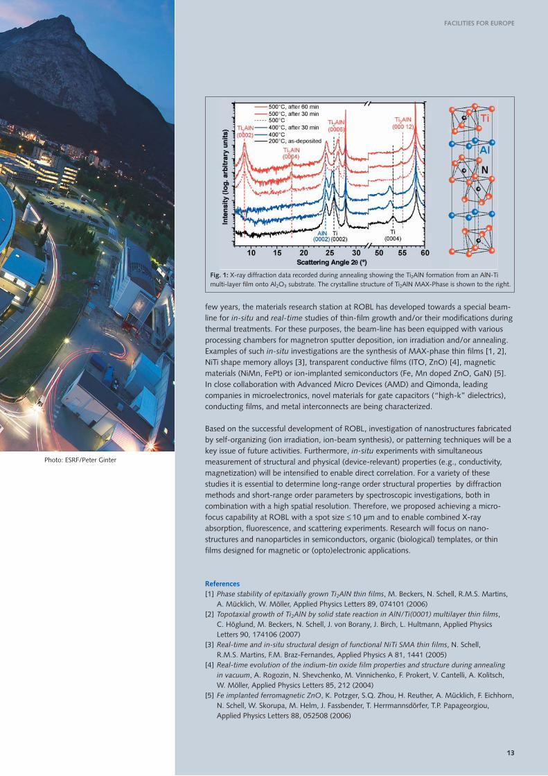
Fig. 1: X-ray diffraction data recorded during annealing showing the Ti2AlN formation from an AlN-Timulti-layer film onto Al2O3 substrate. The crystalline structure of Ti2AlN MAX-Phase is shown to the right.
few years, the materials research station at ROBL has developed towards a special beam-line for in-situ and real-time studies of thin-film growth and/or their modifications duringthermal treatments. For these purposes, the beam-line has been equipped with variousprocessing chambers for magnetron sputter deposition, ion irradiation and/or annealing.Examples of such in-situ investigations are the synthesis of MAX-phase thin films [1, 2],NiTi shape memory alloys [3], transparent conductive films (ITO, ZnO) [4], magneticmaterials (NiMn, FePt) or ion-implanted semiconductors (Fe, Mn doped ZnO, GaN) [5].In close collaboration with Advanced Micro Devices (AMD) and Qimonda, leadingcompanies in microelectronics, novel materials for gate capacitors (“high-k” dielectrics),conducting films, and metal interconnects are being characterized.
Based on the successful development of ROBL, investigation of nanostructures fabricatedby self-organizing (ion irradiation, ion-beam synthesis), or patterning techniques will be akey issue of future activities. Furthermore, in-situ experiments with simultaneousmeasurement of structural and physical (device-relevant) properties (e.g., conductivity,magnetization) will be intensified to enable direct correlation. For a variety of thesestudies it is essential to determine long-range order structural properties by diffractionmethods and short-range order parameters by spectroscopic investigations, both incombination with a high spatial resolution. Therefore, we proposed achieving a micro-focus capability at ROBL with a spot size ≤ 10 µm and to enable combined X-rayabsorption, fluorescence, and scattering experiments. Research will focus on nano-structures and nanoparticles in semiconductors, organic (biological) templates, or thinfilms designed for magnetic or (opto)electronic applications.
References[1] Phase stability of epitaxially grown Ti2AlN thin films, M. Beckers, N. Schell, R.M.S. Martins,
A. Mücklich, W. Möller, Applied Physics Letters 89, 074101 (2006)[2] Topotaxial growth of Ti2AlN by solid state reaction in AlN/Ti(0001) multilayer thin films,
C. Höglund, M. Beckers, N. Schell, J. von Borany, J. Birch, L. Hultmann, Applied Physics Letters 90, 174106 (2007)
[3] Real-time and in-situ structural design of functional NiTi SMA thin films, N. Schell, R.M.S. Martins, F.M. Braz-Fernandes, Applied Physics A 81, 1441 (2005)
[4] Real-time evolution of the indium-tin oxide film properties and structure during annealing in vacuum, A. Rogozin, N. Shevchenko, M. Vinnichenko, F. Prokert, V. Cantelli, A. Kolitsch, W. Möller, Applied Physics Letters 85, 212 (2004)
[5] Fe implanted ferromagnetic ZnO, K. Potzger, S.Q. Zhou, H. Reuther, A. Mücklich, F. Eichhorn,N. Schell, W. Skorupa, M. Helm, J. Fassbender, T. Herrmannsdörfer, T.P. Papageorgiou, Applied Physics Letters 88, 052508 (2006)
Photo: ESRF/Peter Ginter
RESEARCH INSTITUTE OF RADIATION PHYSICS
14
Frank Dohrmann, Burkhard Kämpfer
We need more mass!The mass of objects that surround us in ourmaterial world is essentially made up ofnucleons, i.e., protons and neutrons.Protons and neutrons belong to a group ofparticles that are called hadrons (fromGreek, hadros = heavy, strong) due to theirheaviness and strong interaction. Althoughwe know the numerical values of theseparticle masses with high accuracy, it is notcompletely clear to modern physicists whyparticles actually have a mass. For instance,we do not know why an electron has aspecific mass. Nor do we know why somequarks, which together with gluons makeup the nucleon, have such a small mass: upand down quarks are relatively light (theirmasses are about a hundred times smallerthan the mass of a nucleon). What’s more,gluons do not have any mass at all.
Not only in the microcosm, but also in themacrocosm we are challenged tounderstand mass and energy. Since 1999,astronomical observations have revealedthat the objects in the sky (stars, nebulae,galaxies, and clusters thereof) constituteonly a small fraction of the mattercontained in the universe. Indeed, mostmatter exists in forms which are unknownto us. Therefore, we call them “darkenergy” and “dark matter”, but we knowalmost nothing about them.
All these phenomena provide a strongmotivation for physicists to understand theorigin of the mass of nucleon matter. Thekey to this seems to be the stronginteraction among constituents ofnucleons. In a fictitious world, withmassless quarks, the mass of nucleons andthus, atomic nuclei would only be 20 %smaller than in our real world.
Strange probesExperiments addressing these questionsoften require specific probes. These aretest particles that are created by collisionsin the laboratory.
Kaons (K±) have distinct properties whichallow them to behave differently fromother hadrons. Due to this, they wereoriginally called “strange” hadrons. K± canbe produced through collisions of nuclei.Once the electron orbitals of an atom arestripped in this process, the remainingcharged nucleus (ion) may be accelerated,and an ion beam eventually impinges ontarget nuclei. The kinetic energy of thesecolliding nuclei is partially converted intothe mass of newly produced particles. It isimportant to mention that for nucleus-nucleus collisions, K+ or K– are producedinside the nuclear medium. Upon collision,the nuclear matter of both nuclei iscompressed and heated up; nucleons ofthe nuclei are mixed and they form afireball in which a few newly producedparticles are immersed.
The compression stage, subsequentexpansion, and final disintegration only lastfor about 3 x 10-23 seconds in total. Due tothis short time scale for the violentevolution of the fireball, theoreticalinterpretation is difficult. Therefore, afterinitial experiments with beams of nucleiand nuclear targets, it was necessary toperform a series of experiments in which aproton beam hit a nuclear target andproduced K±. The surrounding nuclearmatter, through which the K± have topenetrate, behaves almost statically. Theinterpretation of such experiments issophisticated. They were carried out by the Kaon Spectrometer (KaoS)collaboration [1], a group of scientists fromFZD, Technische Universität Darmstadt,Universität Frankfurt, Gesellschaft für
Schwerionenforschung Darmstadt,Jagiellonian University Krakow, andUniversität Marburg. The experiments ledto the conclusion that a K- is modified innuclear matter. It may thus be describedeffectively as an excitation with a massreduced by 80 MeV relative to its vacuummass, while the K+ mass is effectivelyincreased by 20 MeV. K+ are alwaysproduced together with a �� hyperon [2].
Di-electrons – Direct messengersIn experiments using K± mesons, thesemay mix in nuclear matter with otherexcitations with the same quantumnumbers as K±. Thus, some information islost and the most interesting spectraldistribution is barely accessible. In contrast,light vector mesons, ρ and ω—anothergroup of hadrons—are better penetratingprobes. A vector meson may decay into anelectron-positron (e+e-) pair, which is calleda di-electron. Measuring the momenta ofe+ and e- yields access to the spectraldistribution of ρ and ω mesons. e+ and e-
only interact electromagnetically withnuclear matter. This interaction is so weakthat the e+e- pair leaves the nuclearmedium nearly undisturbed, thus, carryingthe desired original information, which isneeded for unravelling how the parenthadrons ρ and ω acquire their masses.
Although this approach appears verypromising, a number of experimentalchallenges have to be tackled when usingthese direct probes: (i) only in one out of105 (104) cases does a ρ (ω) meson decayinto an e+e- pair. (ii) At energies, where ρand ω mesons are produced, many othersources of e+e- pairs are generatedunintentionally as well. (iii) The e+ and e-
must be carefully separated from all othercharged particles which occur much morefrequently.
Hadron mass: Why so heavy?Research
15
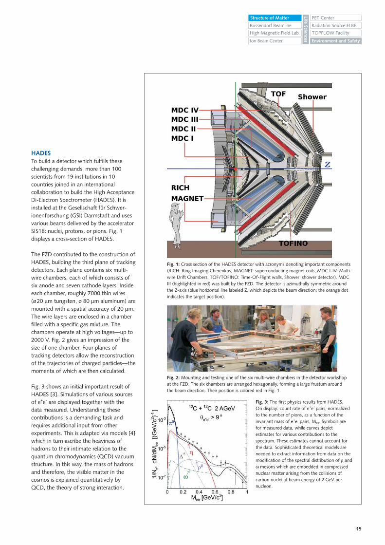
HADESTo build a detector which fulfills thesechallenging demands, more than 100scientists from 19 institutions in 10countries joined in an internationalcollaboration to build the High AcceptanceDi-Electron Spectrometer (HADES). It isinstalled at the Gesellschaft für Schwer-ionenforschung (GSI) Darmstadt and usesvarious beams delivered by the acceleratorSIS18: nuclei, protons, or pions. Fig. 1displays a cross-section of HADES.
The FZD contributed to the construction ofHADES, building the third plane of trackingdetectors. Each plane contains six multi-wire chambers, each of which consists ofsix anode and seven cathode layers. Insideeach chamber, roughly 7000 thin wires(ø20 µm tungsten, ø 80 µm aluminum) aremounted with a spatial accuracy of 20 µm.The wire layers are enclosed in a chamberfilled with a specific gas mixture. Thechambers operate at high voltages—up to2000 V. Fig. 2 gives an impression of thesize of one chamber. Four planes oftracking detectors allow the reconstructionof the trajectories of charged particles—themomenta of which are then calculated.
Fig. 3 shows an initial important result ofHADES [3]. Simulations of various sourcesof e+e- are displayed together with thedata measured. Understanding thesecontributions is a demanding task andrequires additional input from otherexperiments. This is adapted via models [4]which in turn ascribe the heaviness ofhadrons to their intimate relation to thequantum chromodynamics (QCD) vacuumstructure. In this way, the mass of hadronsand therefore, the visible matter in thecosmos is explained quantitatively byQCD, the theory of strong interaction.
Fig. 1: Cross section of the HADES detector with acronyms denoting important components(RICH: Ring Imaging Cherenkov, MAGNET: superconducting magnet coils, MDC I-IV: Multi-wire Drift Chambers, TOF/TOFINO: Time-Of-Flight walls, Shower: shower detector). MDCIII (highlighted in red) was built by the FZD. The detector is azimuthally symmetric aroundthe Z-axis (blue horizontal line labeled Z, which depicts the beam direction; the orange dotindicates the target position).
Fig. 3: The first physics results from HADES. On display: count rate of e+e- pairs, normalizedto the number of pions, as a function of theinvariant mass of e+e- pairs, Mee. Symbols arefor measured data, while curves depictestimates for various contributions to thespectrum. These estimates cannot account forthe data. Sophisticated theoretical models areneeded to extract information from data on themodification of the spectral distribution of ρ andω mesons which are embedded in compressednuclear matter arising from the collisions ofcarbon nuclei at beam energy of 2 GeV pernucleon.
Fig. 2: Mounting and testing one of the six multi-wire chambers in the detector workshopat the FZD. The six chambers are arranged hexagonally, forming a large frustum aroundthe beam direction. Their position is colored red in Fig. 1.
Rossendorf Beamline
Environment and Safety
Structure of Matter
Life Sciences
TOPFLOW FacilityHigh Magnetic Field Lab.
PET Center
Ion Beam Center
Radiation Source ELBE
RESEARCH INSTITUTE OF RADIATION PHYSICS
16
Charming prospectsThe results of KaoS and HADES haveopened the door to answering thequestion about the origin of the masses ofhadrons. New opportunities will soon existto research much-needed supplementaryinformation from the Facility for Anti-proton and Ion Research (FAIR) which isunder construction in Darmstadt. Amongthe core experiments of FAIR are nucleus-nucleus collisions. The accelerator SIS300will deliver ion beams in an energy regionin which the maximum compression ofnuclear matter is expected. Moreover, FAIRprovides a new degree of freedom: charm.Similarly to kaons, which are characterizedby strangeness, D mesons carry a charmquark content. This makes them a very
sensitive probe of the external stronginteraction field and complements theinformation obtained from HADES andKaoS. Using this hadronic probe, furtherdetailed insight into the complexarchitecture of hadrons and their massgeneration is expected.
A large international collaboration hasresulted in the building of the CompressedBaryon Matter (CBM) experiment at theFAIR site in Darmstadt. The task of theRossendorf group is to develop ResistivePlate Chambers (RPC)—modern detectorswith a time resolution shorter than 100 ps.They must function even at very highparticle rates.
Due to the excellent timing properties ofits electron beam (<5 ps resolution), thetime resolution of RPCs is tested usingelectrons from the FZD linac ELBE.Moreover, the intensity of ELBE’s electronbeam offers an extremely valuable tool fortesting the rate capability of moderndetectors. Various test series withprototypes were already conducted atELBE with promising results [5]. Thisnecessary progress in instrumentation alsoprovides cost-saving tools with applicationpotential, e.g., for imaging devices inmedicine. In this way, technology transferand development is accomplished whilethe primary goal of addressingfundamental problems of physics, such asthe heaviness of hadrons, especiallyprotons and neutrons, is also tackled.
References*[1] First observation of in-medium effects
on phase space distributions of antikaons measured in proton-nucleus collisions, W. Scheinast et al. (KaoS Collaboration), Physical Review Letters 96, 072301 (2006)
[2] Angular distributions for 3, 4He bound states in the 3, 4He (e, e’ K+) reaction, F. Dohrmann et al. (E91-016 Collabo-ration), Physical Review Letters 93, 242501 (2004)
[3] Dielectron production in C12+C12 collisions at 2 AGeV with HADES,G. Agakishiev et al. (HADES Collabo-ration), Physical Review Letters 98, 052302 (2007)
[4] Evidence for in-medium changes of four-quark condensates, R. Thomas, S. Zschocke, B. Kämpfer, Physical Review Letters 95, 232301 (2005)
[5] Testing timing RPC detectors at the Rossendorf electron linac ELBE, R. Kotte, F. Dohrmann, J. Hutsch, L. Naumann, D. Stach, Nuclear Instruments and Methods A 654, 155 (2006)
*In this report we quote mainly the most important papers that were published by FZD scientists and their partners.
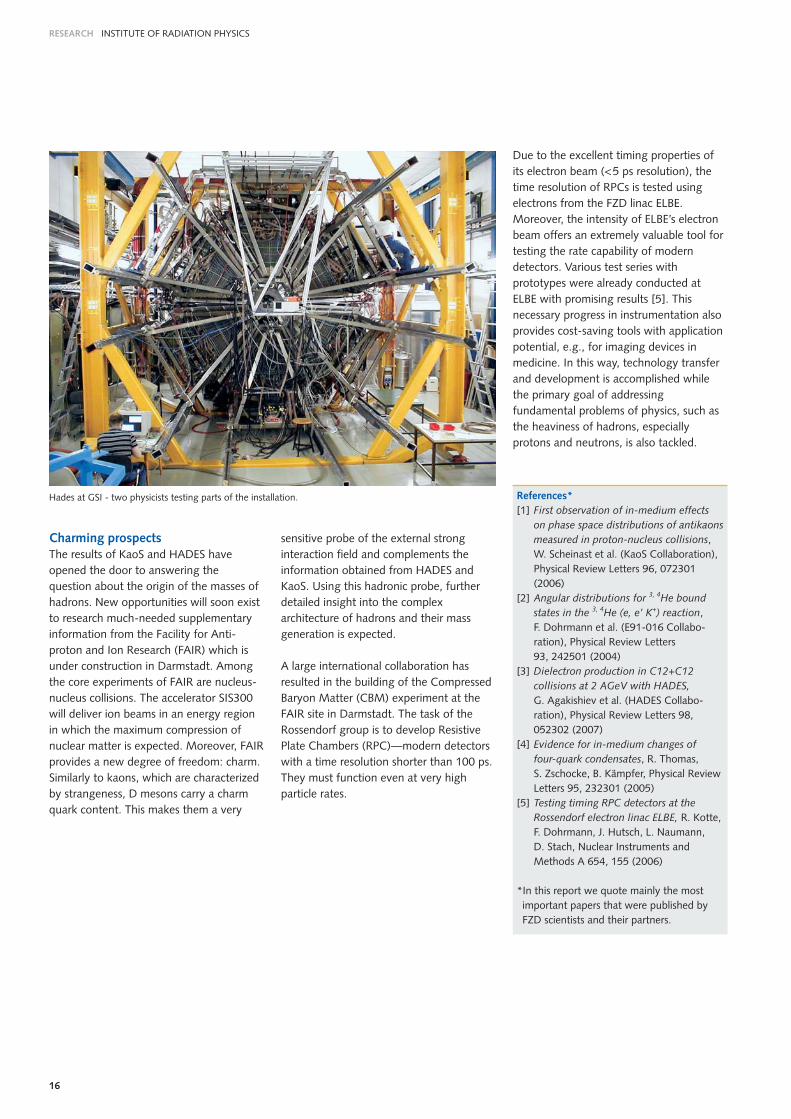
Hades at GSI - two physicists testing parts of the installation.

17
Andreas Wagner, Arnd Junghans, Ronald Schwengner
Heavy chemical elements in the cosmosare produced by fusion reactions of twolight atomic nuclei or by neutron-captureprocesses. Neutron-capture processes inred giant stars produce about half of allnuclei from iron to lead. The other half isproduced during supernova explosions,which occur when heavy stars end their lifecycle. During these cataclysmic eventsgenerating explosions brighter than anentire galaxy [1], rapid neutron captureprocesses and nuclear disintegration byphotons lead to the formation of allelements in our solar system which areheavier than iron. Chemical elements withseveral stable isotopes serve as probes forour understanding of the cosmicnucleosynthesis by using their abundancesas fingerprints of the various productionprocesses. The origin of 35 neutron-deficient isotopes, for example aroundMolybdenum and Samarium, remainsespecially mysterious, as they are bypassedby stellar neutron-capture processes.
Recently, the question of nucleardisintegration induced by the high-temperature photon field present duringsupernova explosions has received growingattention. During these explosions, theouter layers of the exploding star areheated up to several billion Kelvin,extending the thermal photon spectrumbeyond the neutron or proton separationenergy of heavy nuclei. Under theseconditions, the nucleosynthesis pathproceeds through photodisintegrationreactions as shown in Fig. 1.
Creating a supernova photonspectrum with ELBE bremsstrahlung At the FZD Radiation Source ELBE, thethermal photon bath for temperatures of afew billion Kelvin can be replicated usingelectron bremsstrahlung. Scattered from ametal foil, the electron beam generates an
intense continuum of γ-rays similar inenergy to the field of γ-rays in a supernovaas shown in Fig. 2. The ELBE γ-rays arethen used to study nuclear reactions byexperiments which aim at verifying orfalsifying the input of nuclear theory forkey astrophysical cases. In order to study
ELBE γγ-rays shed light on the origin of the chemical elements
Fig. 1: Material driven outwards by the winds from supernova remnant Cassiopeia A (photo: courtesy ofHubble-STScI). The overlay indicates those nuclei studied at the FZD Radiation Source ELBE in the path ofvarious nucleosynthesis reactions.
Fig. 2: Thermal distribution ofphotons at a typical supernovatemperature of three billionKelvin (red line) shown togetherwith the bremsstrahlung at ELBE(blue line) in arbitrary units. The overlay of these two spectratogether with a predicted nuclearphoto-effect cross section showsthat the region of interest can bescanned with bremsstrahlung ofdifferent end point energy.
Rossendorf Beamline
Environment and Safety
Structure of Matter
Life Sciences
TOPFLOW FacilityHigh Magnetic Field Lab.
PET Center
Ion Beam Center
Radiation Source ELBE
the rare processes involved in γ-ray-induced cosmic nucleosynthesis, theuniquely high intensity of the ELBEradiation is necessary to get a sufficientlystrong measurement signal.
One focus of the ELBE experiments is therole of the giant dipole resonance inphoton-induced processes. The giantdipole resonance is the most importantcollective vibration of atomic nuclei.Sufficiently high photon energies lead
to a strong absorption of photons in acharacteristic energy interval. The cosmicnucleosynthesis is most sensitive to the lowenergy side of the giant dipole resonance.Thus, photon absorption directly above theenergy threshold of the nuclear photo-effect, but below the peak of the giantdipole resonance, is particularly important.However, cross sections close to thethreshold are small and difficult tomeasure. The detectors at ELBE which are used to measure the decay of irradiated
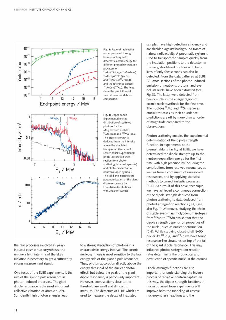
samples have high detection efficiency andare shielded against background traces ofnatural radioactivity. A pneumatic system isused to transport the samples quickly fromthe irradiation positions to the detector. Inthis way, short-lived nuclides with half-lives of only few seconds can also bedetected. From the data gathered at ELBE[2], cross-sections of the photon-inducedemission of neutrons, protons, and evenhelium nuclei have been extracted (seeFig. 3). The latter were detected fromheavy nuclei in the energy region ofcosmic nucleosynthesis for the first time.The nuclides 92Mo and 144Sm serve ascrucial test cases as their abundancepredictions are off by more than an orderof magnitude compared to theobservations.
Photon scattering enables the experimentaldetermination of the dipole strengthfunction. In experiments at thebremsstrahlung facility at ELBE, we havedetermined the dipole strength up to theneutron-separation energy for the firsttime with high precision by including thecontributions from resolved resonances aswell as from a continuum of unresolvedresonances, and by applying statisticalmethods to correct inelastic processes[3,4]. As a result of this novel technique,we have achieved a continuous connectionof the dipole strength deduced fromphoton scattering to data deduced fromphotodisintegration reactions [3,4] (seealso Fig. 4). Moreover, studying the chainof stable even-mass molybdenum isotopesfrom 92Mo to 100Mo has shown that thedipole strength depends on properties ofthe nuclei, such as nuclear deformation[5,6]. While studying closed-shell N=50nuclei like 88Sr [4] and 90Zr, we have foundresonance-like structures on top of the tailof the giant dipole resonance. This mayinfluence photodisintegration reactionrates determining the production anddestruction of specific nuclei in the cosmos.
Dipole-strength functions are alsoimportant for understanding the inverseprocess of radiative neutron capture. Inthis way, the dipole-strength functions innuclei obtained from experiments willimprove both the modeling of cosmicnucleosynthesis reactions and the
RESEARCH INSTITUTE OF RADIATION PHYSICS
18
Fig. 3: Ratio of radioactivenuclei produced throughbremsstrahlung withdifferent electron energy fordifferent photodisintegrationprocesses on 92Mo (92Mo(γ,n)91Mo (blue)92Mo(γ,p)91Nb (green), and 92Mo(γ,α)88Zr (red), and the reference process197Au(γ,n)196Au). The linesshow the predictions of two different models forcomparison.
Fig. 4: Upper panel:Experimental energydistribution of scatteredphotons for theMolybdenum nuclides 98Mo (red) and 100Mo (blue).The dipole strength isdeduced from the intensityabove the simulatedbackground (black line).Lower panel: Experimentalphoto-absorption cross-section from photonscattering data (full symbols)and photo-production ofneutrons (open symbols).The solid line indicates theparameterization of the giantdipole resonance byLorentzian distributions with constant widths.
19
determination of cross sections of neutron-capture reactions which may be used fortransmutation processes. In ourexperiments, atomic nuclei were madevisible through their fluorescence light inthe ELBE bremsstrahlung: they shine with acontinuous spectrum in the ultra-far violetwith a contribution from sharp resonance.
The experiments at ELBE arecomplemented by measurements withradioactive nuclei which are only possibleat the Gesellschaft für Schwerionen-forschung (GSI) in Darmstadt. Thedisintegration of nuclei in the electro-magnetic field of a heavy target nucleus athigh beam energies is used to determinethe electromagnetic-strength function ofnuclei with half-lives down to milliseconds.In conducting these measurements, wecollaborate with GSI Darmstadt, the
Institute of Nuclear Physics atForschungszentrum Karlsruhe, and theInstitute of Nuclear Physics at TechnischeUniversität Darmstadt. The analysis is stillin progress. Collaboration also exists with a group of Konan University in Kobe,Japan, which uses Laser Comptonbackscattered photons to investigatephotodisintegration reactions.
Fostering scientific exchange on thequestions of explosive nuclear synthesisdescribed here, the Institute of RadiationPhysics of the FZD organized theInternational Europhysics Conference“Nuclear Physics in Astrophysics III” inDresden in March 2007. The conferencehighlighted the importance of the input ofnuclear physics to astrophysical modelingand initiated many fruitful scientificdiscussions.
Andreas Wagner preparing an astrophysical experiment.
References[1] The physics of core-collapse supernovae,
S. Woosley, T. Janka, Nature Physics 1, 147 (2006)
[2] Photodissociation of p-process nuclei studied by bremsstrahlung-induced activation, M. Erhard, A.R. Junghans, R. Beyer, E. Grosse1, J. Klug, K. Kosev, C. Nair, N. Nankov, G. Rusev, K.D. Schilling, R. Schwengner, A. Wagner, European Physical Journal A 27, s01, 135 (2006)
[3] Pygmy dipole strength close to particle-separation energies – the case of the Mo isotopes, G. Rusev, E. Grosse1, M. Erhard, A. Junghans, K. Kosev, K.D. Schilling, R. Schwengner, A. Wagner, European Physical Journal A27, s01, 171 (2006)
[4] Dipole response of 88Sr up to the neutron-separation energy, R. Schwengner, G. Rusev, N. Benouaret, R. Beyer, M. Erhard, E. Grosse1, A.R. Junghans, J. Klug, K. Kosev, N. Kostov, C. Nair, N. Nankov, K.D. Schilling, A. Wagner, Physical Review C 76, 034321 (2007)
[5] Systematics of magnetic dipole strength in the stable even-mass Mo isotopes, G. Rusev, R. Schwengner, F. Dönau, M. Erhard, S. Frauendorf, E. Grosse1, A.R. Junghans, L. Käubler, K. Kosev, L.K. Kostov, S. Mallion, K.D. Schilling, A. Wagner, H. von Garrel2, U. Kneissl2, C. Kohstall2, M. Kreutz2, H.H. Pitz2, M. Scheck2, F. Stedile2, P. von Brentano3, J. Jolie3, A. Linnemann3, N. Pietralla3, V. Werner3, Physical Review C 73, 44308 (2006)
[6] Effect of nuclear deformation on the electric-dipole strength in the particle-emission threshold region, F. Dönau, G. Rusev, R. Schwengner, A.R. Junghans, K.D. Schilling, A. Wagner, Physical Review C 76, 014317 (2007)
Project partners1Institute of Nuclear and Particle Physics, Technische Universität Dresden, Germany
2Universität Stuttgart, Germany3University of Cologne, Germany
Charles University in Prague, Czech Republic
Rossendorf Beamline
Environment and Safety
Structure of Matter
Life Sciences
TOPFLOW FacilityHigh Magnetic Field Lab.
PET Center
Ion Beam Center
Radiation Source ELBE
RESEARCH INSTITUTE OF RADIATION PHYSICS · INSTITUTE OF SAFETY RESEARCH
20
Arnd Junghans, Andreas Wagner, Frank-Peter Weiss, Eckart Grosse
One—for many the strongest—of thearguments against a long-term commit-ment to nuclear power as an energy sourceis the need to permanently dispose of thelong-term radioactive waste produced innuclear reactors. Thus, significant effortsare being made worldwide in order tominimize, manage, and dispose of highlyradioactive nuclear waste. Partitioning ofnuclear waste and transmutation of long-lived isotopes into nuclides with a shorterlifetime are being investigated in theEURATOM FP6 program. Several trans-mutation schemes have been proposedand detailed numerical simulations areunderway for an optimal solution.Regarding the development of newconcepts to produce less waste via veryhigh burn-up, different designs involvingcritical reactors or sub-critical accelerator-driven systems (ADS) are being studied in
view of their transmutation capabilities.The Generation IV (Gen-IV) InternationalForum (GIF) has selected six nuclearenergy systems which require additionalresearch and development in order toconfirm their viability. Also, their expectedperformance is to be demonstrated which,among other things, aims at producing lesswaste.
Different schemes have been proposedwhich may considerably reduce theradioactivity of the spent fuel after burn-up. Studies choosing the best optionsmake extensive use of simulation methodsin order to predict the system behavior in agreat variety of possible configurations andrunning conditions. A fundamentalprerequisite for these Monte Carlocomputing techniques is the availability ofreliable cross-section data. This is neededfor processes and operating parameterswhich significantly differ from those ofcurrently used operating systems.
Neutron time-of-flight at ELBEIn particular, accurate knowledge ofneutron-induced nuclear reactions atappropriate energies is crucially importantfor predicting the capabilities of newsystems. This means that for detailedwaste-transmutation research and designwork on Gen-IV systems, energy-dispersive studies are needed. Todetermine neutron energy, the time-of-flight method can be applied to a widerange of energies: starting with a broadspectrum, the neutrons are taggedaccording to their energy by measuringtheir velocity. The FZD Radiation SourceELBE with its ultra-short electron bunchesis especially well suited for this method andtime-of-flight measurements with highresolution can be performed here even forfast neutrons.
Regarding waste reduction, the possibleuse of fast (i.e., un-moderated) neutronsas they come directly from the fissionprocess is highly important. The strongprocesses induced by these fast neutronsare known in principle, but reliablepredictions of the relevant physicalprocesses and phenomena depend on theavailability of high-quality nuclear data. Asthe fission neutron spectrum bears greatresemblance to the neutron distributionoriginating from the nuclear photo effect,a high-intensity electron beam, like theone at ELBE, allows cross-sectionmeasurements for capture and scatteringof fast neutrons by structural materials,fuel and waste from fast reactors. Theneutrons are generated by bombardinghigh atomic number material withelectrons and thus producing brems-strahlung which in turn causes the same material to emit neutrons.
nELBE: Novel research on transmutation of radioactive waste
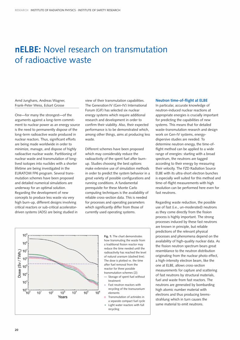
Fig. 1: The chart demonstrateshow transmuting the waste froma traditional fission reactor mayreduce the time needed until theradioactivity has reached the levelof natural uranium (dashed line).The dose is plotted vs. the timeafter fuel removal from thereactor for three possibletransmutation schemes [2]: — Storage of spent fuel without
treatment+ Fast neutron reactors with
recycling of the transuranium elements
o Transmutation of actinides in a separate compact fuel cycle
* Light water reactors with full recycling
21
Obviously the neutron flux, whichdetermines the statistical accuracy of across-section measurement carried out in agiven time, depends on the primary beamintensity and on the amount of convertertarget material put in the beam. At ELBE,flux as a limiting factor is restricted by themaximum beam power accepted on theneutron producing target; however, it isnot limited by the available beam currentfrom the accelerator. A technologicallyinnovative solution for neutron converterssuited for very high beam powerdeposition based on a molten-lead circuit(≈ 5 kW/g) was designed in a collaborativeeffort of the FZD Institutes of RadiationPhysics and Safety Research.
The most important feature of this source,which is advantageous for transmutation-related measurements, is its extremely highflux at a reasonable time resolution: theneutron density of more than 107 n/cm3
produced in the radiator by each micropulse (at ≈ 1 MHz) results in nearly107 n/(s·cm2) at a flight path of roughly
5 m. By making use of the new super-conducting RF-photo-gun at ELBE, therepetition rate can be adjusted to theneutron energy range studied at the givenflight path. Due to the uniquely highbunch charge of up to 2 nC of this electrongun, the full neutron flux is available forneutron energies above 20 keV.
ELBE is the first superconducting electronlinac combined with a neutron time-of-flight facility. A large advantage is that theradio frequency is permanently present,which allows accelerating nearly any pulserepetition rate delivered by the electrongun. At ≈ 1MeV, a resolution ∆E/E of ≈ 2%may be reached with detectors at ≈ 1 nsresolution. The time resolution of the e-beam is much better. Due to its smalldimension of ≈ 1 cm, the radiatorgenerates n-bunches shorter than 1 ns. The setup is devoted to measurements oftransmutation-relevant data for actinidesas well as for fission fragments. Measure-ments with targets of only 10 mg areplanned.
EU-funded collaborationThe Rossendorf neutron time-of-flightsetup called nELBE is part of the EU-funded Integrated Infrastructure Initiative(I3) “European Facilities for Nuclear DataMeasurements” (EFNUDAT). It has beencreated by a consortium of Europeanexperimental facilities for nuclear datameasurements. Joint Research Activities(JRA) within this I3 are concerned with thecompleteness, comparability, and qualityassurance of the nuclear data produced bythe ten participating institutions in sevenEuropean countries. FZD participates inthree JRAs and heads one which isdedicated to neutron generators andtargets. A major task of this JRA is tooptimize the molten-metal radiator withthe electron beam and to investigate howthis design can eventually improve neutronproduction at the other facilities.
Transnational access to nELBE (as well as tothe other neutron facilities) is supported bythis I3, and some of the participatingpartners will perform experiments there.
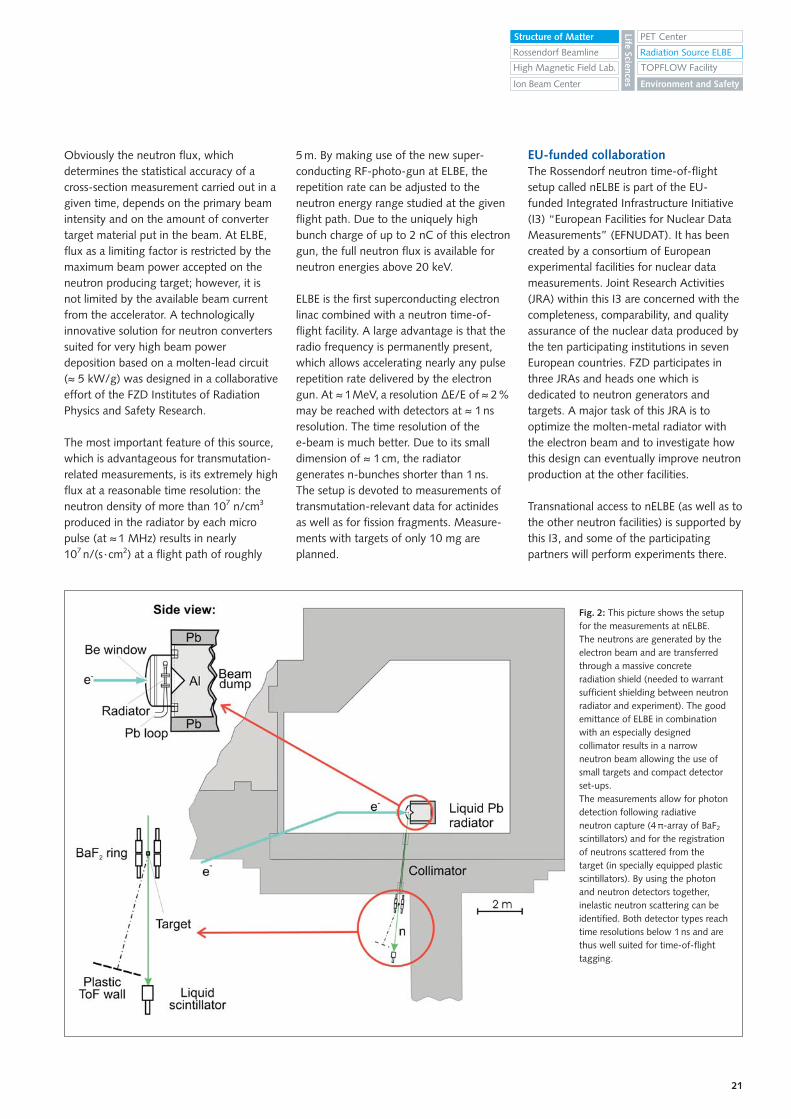
Fig. 2: This picture shows the setupfor the measurements at nELBE. The neutrons are generated by theelectron beam and are transferredthrough a massive concreteradiation shield (needed to warrantsufficient shielding between neutronradiator and experiment). The goodemittance of ELBE in combinationwith an especially designedcollimator results in a narrowneutron beam allowing the use ofsmall targets and compact detectorset-ups.The measurements allow for photondetection following radiativeneutron capture (4 π-array of BaF2
scintillators) and for the registrationof neutrons scattered from thetarget (in specially equipped plasticscintillators). By using the photonand neutron detectors together,inelastic neutron scattering can beidentified. Both detector types reachtime resolutions below 1 ns and arethus well suited for time-of-flighttagging.
Rossendorf Beamline
Environment and Safety
Structure of Matter
Life Sciences
TOPFLOW FacilityHigh Magnetic Field Lab.
PET Center
Ion Beam Center
Radiation Source ELBE
RESEARCH INSTITUTE OF RADIATION PHYSICS · INSTITUTE OF SAFETY RESEARCH
22
The only two other neutron time-of-flightfacilities within EFNUDAT haveconcentrated on slower neutrons in thepast (including moderated, i.e., thermalneutrons). The installation at the EuropeanCommission Institute of ReferenceMaterials and Measurements (IRMM) inGeel has considerably less primary beampower and thus less neutron flux. At theproposed short (20 m) flight path ofCERN/n_TOF, the flux will be somewhatlarger than nELBE in the energy rangeaccessible here, but the energy resolution is expected to be superior at FZD.
The FZD activities in the field of moltenmetal neutron converters parallel similarattempts in the USA and Japan which arecarried out in view of the upcomingSpallation Neutron Source (SNS) and theJapanese Proton Accelerator ResearchComplex J-PARC, respectively. Both arebuilt to deliver significantly higher particlefluxes than available today. The researchperformed at FZD will thus not onlyrepresent a significant step forward toupgrade the nuclear-data measurementswithin the EFNUDAT initiative, but, asmany European scientists in the field ofmaterials research hope, may also lead toresults which can perhaps be used in thefuture European Spallation Source ESS.
References[1] Energiedispersive Untersuchung der
Wechselwirkung schneller Neutronen mit Materie, E. Altstadt, C. Beckert, H. Freiesleben1, V. Galindo, M. Greschner, E. Grosse, A.R. Junghans, B. Naumann, S. Schneider, K. Seidel, F.-P. Weiß, Scientific Technical Report, FZR-426, April 2005; Abschlussbericht DFG-Projekt Gr 1674/2
[2] M. Salvatores, State of the art and perspectives in radioactive waste transmutation; CEA Cadarache 2005
[3] A photo-neutron source for time-of-flight measurements at the radiation source ELBE, E. Altstadt, C. Beckert, E. Grosse, H. Freiesleben1, J. Klug, A.R. Junghans, R. Schlenk, F.-P. Weiss et al., Annals of Nuclear Energy 34, 36 (2007)
[4] Development of a neutron time-of-flight source at the ELBE accelerator, J. Klug, E. Altstadt, C. Beckert, R. Beyer, H. Freiesleben1, V. Galindo, E. Grosse, A.R. Junghans, D. Legrady, B. Naumann, K. Noack, G. Rusev, K.D. Schilling, R. Schlenk, S. Schneider, A. Wagner, F.-P. Weiß, Nuclear Instruments and Methods in Physics Research A 577, 641 (2007)
[5] Proton-recoil detectors for time-of-flight measurements of neutrons with kinetic energies from some tens of keV to a few MeV, R. Beyer, E. Grosse, K. Heidel, J. Hutsch, A.R. Junghans, J. Klug, D. Legrady, R. Nolte, S. Röttger, M. Sobiella, A. Wagner, Nuclear Instruments and Methods in Physics Research A 575, 449 (2007)
Project partners1Institute of Nuclear and Particle Physics, Technische Universität Dresden, Germany
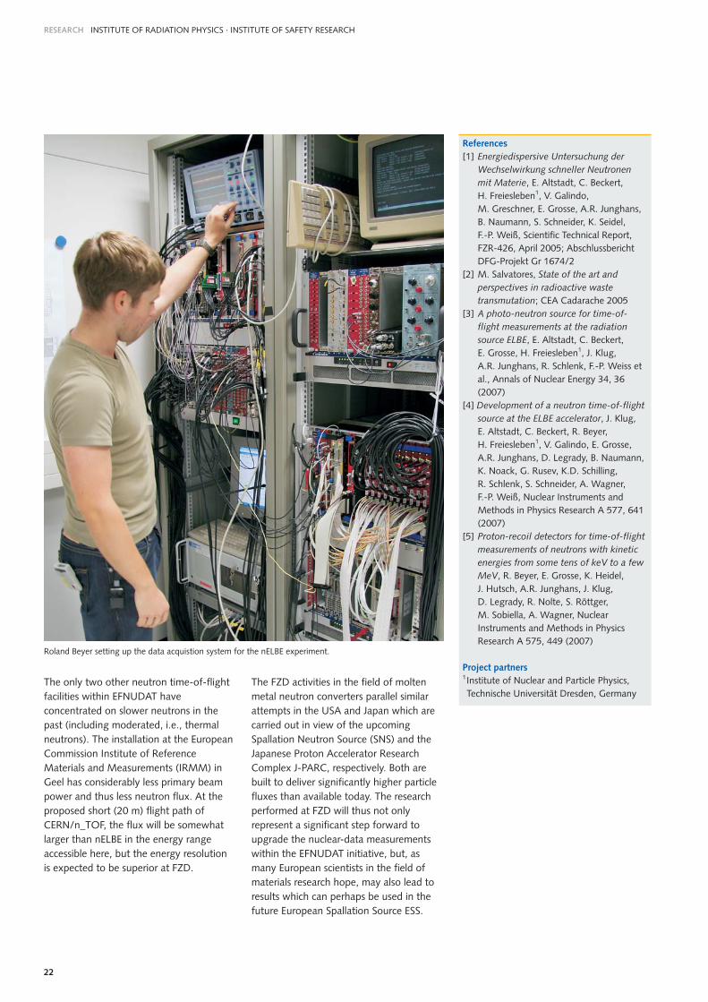
Roland Beyer setting up the data acquistion system for the nELBE experiment.
23
Thomas Herrmannsdörfer
When cooled to low temperatures andexposed to very high magnetic fields, theproperties and behavior of some materialscan dramatically change compared to theirproperties at ambient conditions. Therelevant mechanisms for changing theirelectronic, magnetic, and optical propertiescan be determined better under extremeconditions such as high magnetic fields. Afascinating demonstration of the quantummechanical processes in metallic orsemiconductor materials was performed byW. de Haas, L. Shubnikov, and P. vanAlphen in the early 1930s. Their pioneeringobservation of oscillations of the magneticsusceptibility and electrical resistance of Bias well as other materials in high magneticfields prepared the way for determiningmicroscopic electronic properties ofconductive matter.
Thanks in part to their findings, today weknow in detail how magnetic fields forceconduction electrons in solids or, moreprecisely, in any kind of delocalized chargecarriers on cyclotron orbits. In addition, wehave gained insight into the changes oftheir energy spectrum, previouslyconsidered a continuum, and nowunderstood as a set of quantized highlypopulated energy levels called “Landau”levels. We now understand that anincrease in the magnetic field increases thecyclotron-energy splitting between thelevels linearly as well as the number ofcharge-carrier states per Landau level. As each Landau level passes through theFermi energy at a specific magnetic field, itdepopulates—at the same time increasingthe population of the lower states. Thisperiodic population/depopulation scenarioleads to quantum oscillations of magneticand transport properties. Starting from L.Onsager’s theoretical description in 1952,the monitoring of quantum oscillations in
high magnetic fields has been developedfrom the early days of solid-state physicsto a precise tool for the study of electronicband structures of metallic systems. Withaccess to ever higher magnetic fields, theband structures of more and more classesof materials have been determinedthrough high-field studies. In particular,spectacular changes of the period ofquantum oscillations have been found inthe presence of structural or magneticphase transitions, which also affect theconduction electron density. However,there is plenty still remaining to bediscovered. For example, changes of theband structure, (i.e., of the energydistribution of charge carriers inmomentum space) which are caused solelyby the application of high magnetic fieldshave not yet been observed. In con-ventional materials like copper, silver, orgold, the band structure hardly everchanges—even by applying the highestmagnetic fields.
Quantum phase transitionsin an exotic metal
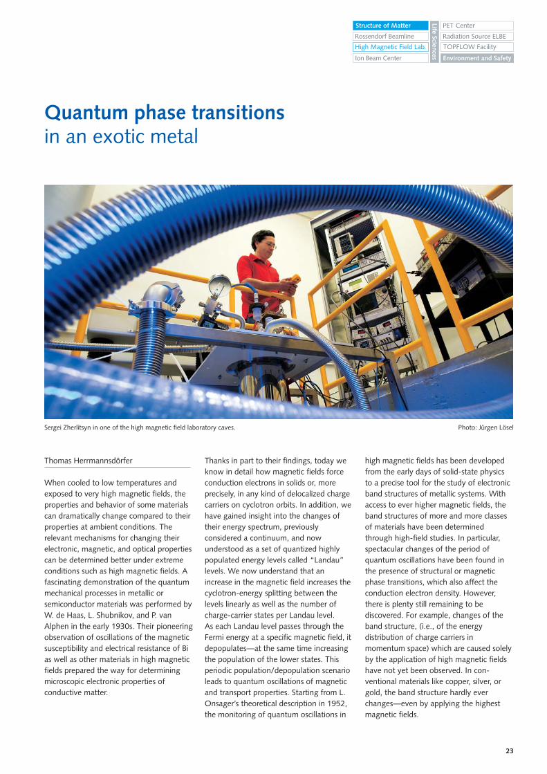
Sergei Zherlitsyn in one of the high magnetic field laboratory caves.
Rossendorf Beamline
Environment and Safety
Structure of Matter
Life Sciences
TOPFLOW FacilityHigh Magnetic Field Lab.
PET Center
Ion Beam Center
Radiation Source ELBE
Photo: Jürgen Lösel
RESEARCH DRESDEN HIGH MAGNETIC FIELD LABORATORY (HLD)
24
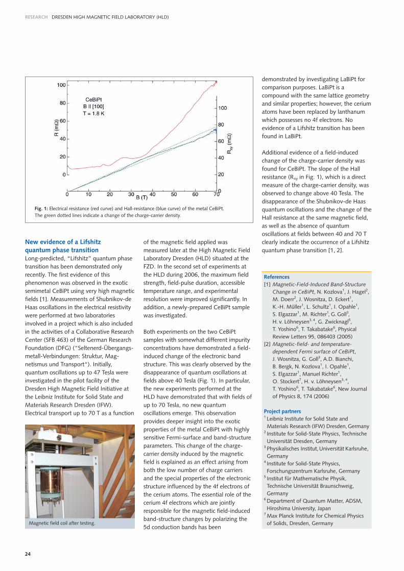
New evidence of a Lifshitz quantum phase transitionLong-predicted, “Lifshitz” quantum phasetransition has been demonstrated onlyrecently. The first evidence of thisphenomenon was observed in the exoticsemimetal CeBiPt using very high magneticfields [1]. Measurements of Shubnikov-deHaas oscillations in the electrical resistivitywere performed at two laboratoriesinvolved in a project which is also includedin the activities of a Collaborative ResearchCenter (SFB 463) of the German ResearchFoundation (DFG) (“Seltenerd-Übergangs-metall-Verbindungen: Struktur, Mag-netismus und Transport“). Initially,quantum oscillations up to 47 Tesla wereinvestigated in the pilot facility of theDresden High Magnetic Field Initiative atthe Leibniz Institute for Solid State andMaterials Research Dresden (IFW).Electrical transport up to 70 T as a function
of the magnetic field applied wasmeasured later at the High Magnetic FieldLaboratory Dresden (HLD) situated at theFZD. In the second set of experiments atthe HLD during 2006, the maximum fieldstrength, field-pulse duration, accessibletemperature range, and experimentalresolution were improved significantly. Inaddition, a newly-prepared CeBiPt samplewas investigated.
Both experiments on the two CeBiPtsamples with somewhat different impurityconcentrations have demonstrated a field-induced change of the electronic bandstructure. This was clearly observed by thedisappearance of quantum oscillations atfields above 40 Tesla (Fig. 1). In particular,the new experiments performed at theHLD have demonstrated that with fields ofup to 70 Tesla, no new quantumoscillations emerge. This observationprovides deeper insight into the exoticproperties of the metal CeBiPt with highlysensitive Fermi-surface and band-structureparameters. This change of the charge-carrier density induced by the magneticfield is explained as an effect arising fromboth the low number of charge carriersand the special properties of the electronicstructure influenced by the 4f electrons ofthe cerium atoms. The essential role of thecerium 4f electrons which are jointlyresponsible for the magnetic field-inducedband-structure changes by polarizing the5d conduction bands has been
demonstrated by investigating LaBiPt forcomparison purposes. LaBiPt is acompound with the same lattice geometryand similar properties; however, the ceriumatoms have been replaced by lanthanumwhich possesses no 4f electrons. Noevidence of a Lifshitz transition has beenfound in LaBiPt.
Additional evidence of a field-inducedchange of the charge-carrier density wasfound for CeBiPt. The slope of the Hallresistance (Rxy in Fig. 1), which is a directmeasure of the charge-carrier density, wasobserved to change above 40 Tesla. Thedisappearance of the Shubnikov-de Haasquantum oscillations and the change of theHall resistance at the same magnetic field,as well as the absence of quantumoscillations at fields between 40 and 70 Tclearly indicate the occurrence of a Lifshitzquantum phase transition [1, 2].
Fig. 1: Electrical resistance (red curve) and Hall-resistance (blue curve) of the metal CeBiPt.The green dotted lines indicate a change of the charge-carrier density.
References[1] Magnetic-Field-Induced Band-Structure
Change in CeBiPt, N. Kozlova1, J. Hagel2,M. Doerr2, J. Wosnitza, D. Eckert1, K.-H. Müller1, L. Schultz1, I. Opahle1, S. Elgazzar1, M. Richter1, G. Goll3,H. v. Löhneysen3, 4, G. Zwicknagl5, T. Yoshino6, T. Takabatake6, Physical Review Letters 95, 086403 (2005)
[2] Magnetic-field- and temperature-dependent Fermi surface of CeBiPt, J. Wosnitza, G. Goll3, A.D. Bianchi, B. Bergk, N. Kozlova1, I. Opahle1, S. Elgazzar1, Manuel Richter1, O. Stockert7, H. v. Löhneysen3, 4, T. Yoshino6, T. Takabatake6, New Journal of Physics 8, 174 (2006)
Project partners1 Leibniz Institute for Solid State and Materials Research (IFW) Dresden, Germany
2 Institute for Solid-State Physics, Technische Universität Dresden, Germany
3 Physikalisches Institut,Universität Karlsruhe, Germany
4 Institute for Solid-State Physics, Forschungszentrum Karlsruhe, Germany
5 Institut für Mathematische Physik, Technische Universität Braunschweig, Germany
6 Department of Quantum Matter, ADSM, Hiroshima University, Japan
7 Max Planck Institute for Chemical Physics of Solids, Dresden, Germany Magnetic field coil after testing.
25
Sergei Zvyagin
Bosons, named after Satyendra Nath Bose,are particles with integer spin. In contrastto fermions (which carry half-integer spin),bosons obey Bose-Einstein statistics. Oneof the most fascinating aspects of theseparticles is the phenomenon of Bose-Einstein condensation (BEC). In this state,an unlimited quantity of bosons can sharethe same quantum state with wavefunctions remaining coherent on themacroscopic scale. The BEC phase, alsoreferred to as the “fifth state of matter”,was first postulated as a consequence ofquantum mechanics by Albert Einstein,building upon the work of Bose in 1925.The Bose-Einstein condensate, and theprocess of condensation itself, waspredicted to have many unusual propertiesand was indeed found to be responsiblefor a number of fascinating phenomena inquantum physics, such as the superfluidityof 4He. For years, scientists have beenlooking for other manifestations of BEC inthe laboratory. Finally, in 1995, conclusiveevidence for BEC in a dilute gas ofrubidium-87 atoms, cooled down totemperatures lower than 1 µK, wasobtained. For this observation, thescientists Cornell, Ketterle, and Wiemanwere awarded the Nobel Prize in Physics in 2001.
Searching for BEC in other bosonicparticles remains a formidable challenge in modern quantum physics. A possibleexample of this phenomenon may befound in the condensation of magneticquasiparticles called magnons intoquantum magnets. For many quantumsystems, the magnetic field tends tosuppress quantum fluctuations, leading toa system with a magnetically well-orderedstate. By changing the magnetic field, themagnon concentration can be controlled.This provides access to a wide range of
Searching for the magnetic Bose-Einstein condensate
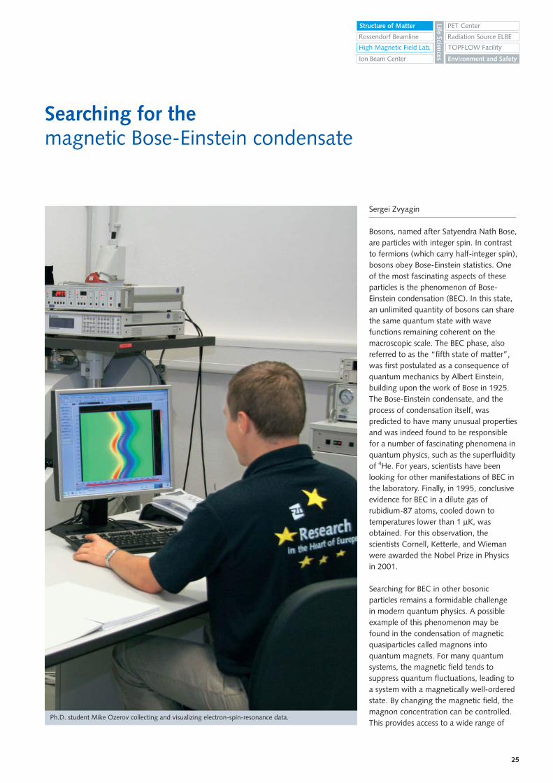
Ph.D. student Mike Ozerov collecting and visualizing electron-spin-resonance data.
Rossendorf Beamline
Environment and Safety
Structure of Matter
Life Sciences
TOPFLOW FacilityHigh Magnetic Field Lab.
PET Center
Ion Beam Center
Radiation Source ELBE
RESEARCH DRESDEN HIGH MAGNETIC FIELD LABORATORY (HLD)
26
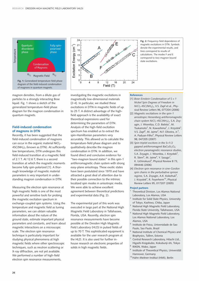
magnon densities, from a dilute gas ofparticles to a strongly interacting Boseliquid. Fig. 1 shows a sketch of thegeneralized temperature-field phasediagram for the magnon condensation inquantum magnets.
Field-induced condensation of magnons in DTNRecently, it has been suggested that thefield-induced condensation of magnonscan occur in the organic material NiCl2-4SC(NH2)2 (known as DTN). At sufficientlylow temperatures, DTN undergoes thisfield-induced transition at a magnetic fieldof 2.1 T. At 12.6 T, there is a secondtransition at which the magnetic momentsbecome fully spin-polarized [1]. A thor-ough knowledge of magnetic materialparameters is very important in under-standing magnon condensation in DTN.
Measuring the electron spin resonance athigh magnetic fields is one of the mostpowerful and sensitive tools for probingthe magnetic excitation spectrum inexchange-coupled spin systems. Using thetemperature and magnetic field as tuningparameters, we can obtain valuableinformation about the nature of theground state, estimate important physicalparameters and constants, and learn aboutmagnetic interactions on a microscopicscale. The electron spin resonancetechnique is particularly important forstudying physical phenomena at highmagnetic fields where other spectroscopictechniques, such as neutron scattering orX-ray diffraction, are not yet available.We performed a number of high-fieldelectron spin resonance measurements,
investigating the magnetic excitations inmagnetically low-dimensional materials [2-4]. In particular, we studied theseexcitations in DTN in magnetic fields of upto 25 T. A distinct advantage of the high-field approach is the availability of exacttheoretical expressions used fordetermining the parameters of DTN.Analysis of the high-field excitationspectrum has enabled us to extract thespin-Hamiltonian parameters veryaccurately. This allowed us to calculate thetemperature-field phase diagram and toqualitatively describe the magnoncondensation in DTN. In addition, wefound direct and conclusive evidence for“two-magnon bound states” in this spin-1antiferromagnetic chain system with strongeasy-plane anisotropy. These exotic stateshave been postulated since 1970 and haveattracted a great deal of attention due totheir possible connection to the intrinsiclocalized spin modes in anisotropic media.We were able to achieve excellentagreement between theoretical predictionsand experimental data (Fig. 2).
The experimental part of this work wasexecuted in large part at the National HighMagnetic Field Laboratory in Tallahassee,Florida, USA. Recently, electron spinresonance measurements have becomepossible at the Dresden High MagneticField Laboratory (HLD) in pulsed fields ofup to 70 T. This sophisticated equipment isavailable for the user research program atthe HLD. It is also used for further in-house research on electronic properties ofsolids in high magnetic fields.
Fig. 1: Generalized temperature-field phasediagram of the field-induced condensationof magnons in quantum magnets.
Fig. 2: Frequency-field dependence ofmagnetic excitations in DTN. Symbolsdenote the experimental results, andlines correspond to results ofcalculations. The modes F and Ecorrespond to two-magnon boundstate excitations.
References[1] Bose-Einstein Condensation of S = 1
Nickel Spin Degrees of Freedom in NiCl2-4SC(NH2)2, V.S. Zapf et al., Phy-sical Review Letters 96, 077204 (2006)
[2] Magnetic excitations in the spin-1 anisotropic Heisenberg antiferromagnetic chain system NiCl2-4SC(NH2)2, S.A. Zvy-agin, J. Wosnitza, C.D. Batista1, M. Tsukamoto2, N. Kawashima2, J. Krzystek3, V.S. Zapf4, M. Jaime4, N.F. Oliveira, Jr.5, A. Paduan-Filho5, Physical Review Letters 98, 047205 (2007)
[3] Spin-triplet excitons in the S=1/2 gapped antiferromagnet BaCuSi2O6: electron paramagnetic resonance studies, S.A. Zvyagin, J. Wosnitza, J. Krzystek3, R. Stern6, M. Jaime4, Y. Sasago7, K. Uchinokura8, Physical Review B 73, 094446 (2006)
[4] Electron spin resonance in sine-Gordon spin chains in the perturbative spinon regime, S.A. Zvyagin, A.K. Kolezhuk9, J. Krzystek3, R. Feyerherm10, Physical Review Letters 95, 017207 (2005)
Project partners1 Theoretical Division, Los Alamos National
Laboratory, Los Alamos, USA2 Institute for Solid State Physics, University
of Tokyo, Kashiwa, Chiba, Japan3 National High Magnetic Field Laboratory,
Florida State University, Tallahassee, USA4 National High Magnetic Field Laboratory,
Los Alamos National Laboratory, Los Alamos, USA
5 Instituto de Fisica, Universidade de Sao Paulo, Sao Paulo, Brazil
6 National Institute of Chemical Physics and Biophysics, Tallinn, Estonia
7 Central Research Laboratory, Hitachi Ltd., Higashi-Koigakubo, Kokubunji-shi, Tokyo
8 RIKEN, Wako, Japan9 Institute of Theoretical Physics, Universität
Hannover, Germany10 Hahn-Meitner-Institut (HMI), Berlin
27
Jürgen Faßbender
The mission of the "nanoscale magnetism"group of the FZD is to understand thefundamental effects which determine themagnetic material properties of nanoscaleelements. For their creation and modi-fication, ion beam technologies are used.In addition to conventional topographicpatterning approaches, pure magneticmaterial modifications on the nanoscaleare emphasized. This way, devices withnew functionalities can be created whichcould be applied in the fields of sensorsand magneto-logic devices. The largevariety of research topics in this area canbe illustrated by three different exampleson which we have been focusing.
Hybrid magnetic materials: microscopic origin – macroscopic resultsWe are investigating the correlationbetween artificially-generated magnetic-domain configurations and effectivemagnetic properties, i. e., magneticanisotropy, exchange coupling, andinterlayer-exchange coupling [1 – 5].Artificial domain structures are producedby means of ion-irradiation techniqueswhich allow modification of the magneticparameters on a length scale similar to oreven below the exchange-correlationlength (typically ~ 10 – 1000 nm). In doingso, completely new domain walls anddomain configurations, which are notpossible in conventional thin films, arecreated. When they are furtherminiaturized, the domains vanish and an“effective” material with new properties,observed neither in fully irradiated nor innon-irradiated films, is designed. These arecalled hybrid materials. Fig. 1 shows anexample of such an artificial magneticdomain configuration. Fig. 1 a) displays a
Ions meet magnets – tailor-made properties on the nano-scale
Kay Potzger adjusting the magnetic force microscope (MFM).
Rossendorf Beamline
Environment and Safety
Structure of Matter
Life Sciences
TOPFLOW FacilityHigh Magnetic Field Lab.
PET Center
Ion Beam Center
Radiation Source ELBE
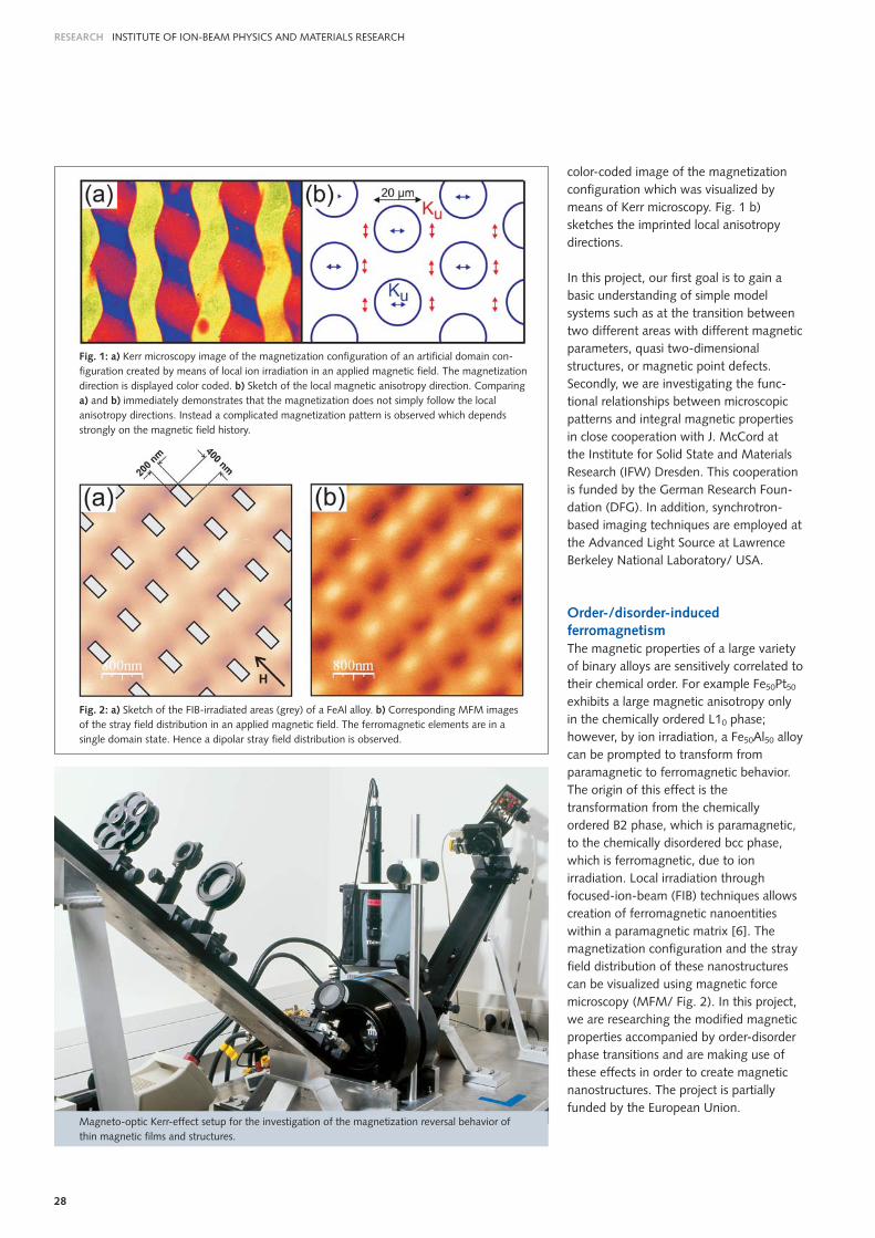
RESEARCH INSTITUTE OF ION-BEAM PHYSICS AND MATERIALS RESEARCH
28
color-coded image of the magnetizationconfiguration which was visualized bymeans of Kerr microscopy. Fig. 1 b)sketches the imprinted local anisotropydirections.
In this project, our first goal is to gain abasic understanding of simple modelsystems such as at the transition betweentwo different areas with different magneticparameters, quasi two-dimensionalstructures, or magnetic point defects.Secondly, we are investigating the func-tional relationships between microscopicpatterns and integral magnetic propertiesin close cooperation with J. McCord at the Institute for Solid State and MaterialsResearch (IFW) Dresden. This cooperationis funded by the German Research Foun-dation (DFG). In addition, synchrotron-based imaging techniques are employed atthe Advanced Light Source at LawrenceBerkeley National Laboratory/ USA.
Order-/disorder-inducedferromagnetismThe magnetic properties of a large varietyof binary alloys are sensitively correlated totheir chemical order. For example Fe50Pt50
exhibits a large magnetic anisotropy onlyin the chemically ordered L10 phase;however, by ion irradiation, a Fe50Al50 alloycan be prompted to transform fromparamagnetic to ferromagnetic behavior.The origin of this effect is thetransformation from the chemicallyordered B2 phase, which is paramagnetic,to the chemically disordered bcc phase,which is ferromagnetic, due to ionirradiation. Local irradiation throughfocused-ion-beam (FIB) techniques allowscreation of ferromagnetic nanoentitieswithin a paramagnetic matrix [6]. Themagnetization configuration and the strayfield distribution of these nanostructurescan be visualized using magnetic forcemicroscopy (MFM/ Fig. 2). In this project,we are researching the modified magneticproperties accompanied by order-disorderphase transitions and are making use ofthese effects in order to create magneticnanostructures. The project is partiallyfunded by the European Union.
Magneto-optic Kerr-effect setup for the investigation of the magnetization reversal behavior ofthin magnetic films and structures.
Fig. 1: a) Kerr microscopy image of the magnetization configuration of an artificial domain con-figuration created by means of local ion irradiation in an applied magnetic field. The magnetizationdirection is displayed color coded. b) Sketch of the local magnetic anisotropy direction. Comparinga) and b) immediately demonstrates that the magnetization does not simply follow the localanisotropy directions. Instead a complicated magnetization pattern is observed which dependsstrongly on the magnetic field history.
Fig. 2: a) Sketch of the FIB-irradiated areas (grey) of a FeAl alloy. b) Corresponding MFM imagesof the stray field distribution in an applied magnetic field. The ferromagnetic elements are in asingle domain state. Hence a dipolar stray field distribution is observed.
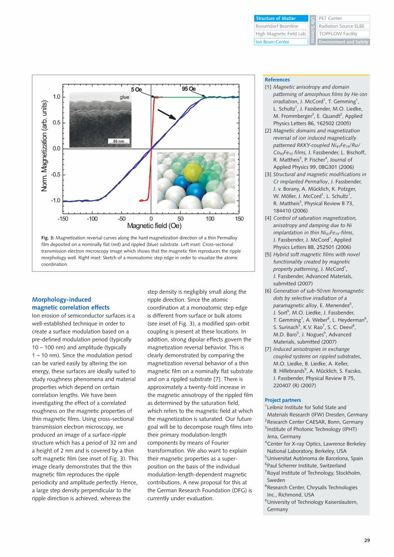
29
Morphology-induced magnetic correlation effectsIon erosion of semiconductor surfaces is awell-established technique in order tocreate a surface modulation based on apre-defined modulation period (typically10 – 100 nm) and amplitude (typically 1 – 10 nm). Since the modulation periodcan be varied easily by altering the ionenergy, these surfaces are ideally suited tostudy roughness phenomena and materialproperties which depend on certaincorrelation lengths. We have beeninvestigating the effect of a correlatedroughness on the magnetic properties ofthin magnetic films. Using cross-sectionaltransmission electron microscopy, weproduced an image of a surface-ripplestructure which has a period of 32 nm anda height of 2 nm and is covered by a thinsoft magnetic film (see inset of Fig. 3). Thisimage clearly demonstrates that the thinmagnetic film reproduces the rippleperiodicity and amplitude perfectly. Hence,a large step density perpendicular to theripple direction is achieved, whereas the
step density is negligibly small along theripple direction. Since the atomiccoordination at a monoatomic step edge is different from surface or bulk atoms (see inset of Fig. 3), a modified spin-orbitcoupling is present at these locations. Inaddition, strong dipolar effects govern themagnetization reversal behavior. This isclearly demonstrated by comparing themagnetization reversal behavior of a thinmagnetic film on a nominally flat substrateand on a rippled substrate [7]. There isapproximately a twenty-fold increase inthe magnetic anisotropy of the rippled filmas determined by the saturation field,which refers to the magnetic field at whichthe magnetization is saturated. Our futuregoal will be to decompose rough films intotheir primary modulation-lengthcomponents by means of Fouriertransformation. We also want to explaintheir magnetic properties as a super-position on the basis of the individualmodulation-length-dependent magneticcontributions. A new proposal for this atthe German Research Foundation (DFG) iscurrently under evaluation.
Fig. 3: Magnetization reversal curves along the hard magnetization direction of a thin Permalloyfilm deposited on a nominally flat (red) and rippled (blue) substrate. Left inset: Cross-sectionaltransmission electron microscopy image which shows that the magnetic film reproduces the ripplemorphology well. Right inset: Sketch of a monoatomic step edge in order to visualize the atomiccoordination.
References[1] Magnetic anisotropy and domain
patterning of amorphous films by He-ion irradiation, J. McCord1, T. Gemming1, L. Schultz1, J. Fassbender, M.O. Liedke, M. Frommberger2, E. Quandt2, Applied Physics Letters 86, 162502 (2005)
[2] Magnetic domains and magnetization reversal of ion induced magnetically patterned RKKY-coupled Ni81Fe19/Ru/Co90Fe10 films, J. Fassbender, L. Bischoff, R. Mattheis3, P. Fischer4, Journal of Applied Physics 99, 08G301 (2006)
[3] Structural and magnetic modifications in Cr implanted Permalloy, J. Fassbender, J. v. Borany, A. Mücklich, K. Potzger, W. Möller, J. McCord1, L. Schultz1, R. Mattheis3, Physical Review B 73, 184410 (2006)
[4] Control of saturation magnetization, anisotropy and damping due to Ni implantation in thin Ni81Fe19-films, J. Fassbender, J. McCord1, Applied Physics Letters 88, 252501 (2006)
[5] Hybrid soft magnetic films with novel functionality created by magnetic property patterning, J. McCord1, J. Fassbender, Advanced Materials, submitted (2007)
[6] Generation of sub-50 nm ferromagnetic dots by selective irradiation of a paramagnetic alloy, E. Menendez5, J. Sort5, M.O. Liedke, J. Fassbender, T. Gemming1, A. Weber6, L. Heyderman6, S. Surinach5, K.V. Rao7, S. C. Deevi8, M.D. Baro5, J. Nogues5, Advanced Materials, submitted (2007)
[7] Induced anisotropies in exchange coupled systems on rippled substrates, M.O. Liedke, B. Liedke, A. Keller, B. Hillebrands9, A. Mücklich, S. Facsko, J. Fassbender, Physical Review B 75, 220407 (R) (2007)
Project partners1Leibniz Institute for Solid State and Materials Research (IFW) Dresden, Germany
2Research Center CAESAR, Bonn, Germany3Institute of Photonic Technology (IPHT) Jena, Germany
4Center for X-ray Optics, Lawrence Berkeley National Laboratory, Berkeley, USA
5Universitat Autònoma de Barcelona, Spain6Paul Scherrer Institute, Switzerland7Royal Institute of Technology, Stockholm, Sweden
8Research Center, Chrysalis Technologies Inc., Richmond, USA
9University of Technology Kaiserslautern, Germany
Rossendorf Beamline
Environment and Safety
Structure of Matter
Life Sciences
TOPFLOW FacilityHigh Magnetic Field Lab.
PET Center
Ion Beam Center
Radiation Source ELBE
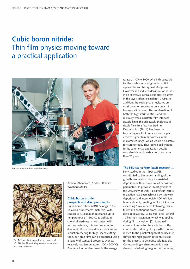
RESEARCH INSTITUTE OF ION-BEAM PHYSICS AND MATERIALS RESEARCH
30
Barbara Abendroth, Andreas Kolitsch,Wolfhard Möller
Cubic boron nitride: prospects and disappointmentsCubic boron nitride (cBN) belongs to theso-called “superhard” materials. Withrespect to its oxidation resistance up totemperatures of 1300 °C as well as itschemical inertness in hot contact withferrous materials, it is even superior todiamond. Thus it would be an ideal wear-reduction coating for high-speed cuttingtools. cBN thin films can be produced usinga variety of standard processes even atrelatively low temperatures (100 – 500 °C).Energetic ion bombardment in the energy
range of 100 to 1000 eV is indispensablefor the nucleation and growth of cBNagainst the soft hexagonal hBN phase.However, ion-induced densification resultsin an excessive intrinsic compressive stressin the layers often exceeding 10 GPa. Inaddition, the cubic phase nucleates onmost common substrates only on a thinhexagonal interlayer. The combination ofboth the high intrinsic stress and therelatively weak substrate/film interfaceusually limits the achievable thickness ofstable films to a few hundred nm.Delamination (Fig. 1) has been thefrustrating result of numerous attempts toachieve higher film thicknesses in themicrometer range, which would be suitablefor cutting tools. Thus, cBN is still waitingfor its commercial application despiteconsiderable worldwide efforts for morethan 20 years.
The FZD story: From basic research…Early studies in the 1990s at FZDcontributed to the understanding of thegrowth mechanism using ion-assisteddeposition with well-controlled depositionparameters. In previous investigations atthe University of Ulm [1], significant stressrelaxation had been achieved by stepwisedeposition and intermediate 300 keV ionbombardment, resulting in film thicknessesexceeding 1 micrometer. Following this, afaster and continuous process wasdeveloped at FZD, using mid-level (several10 keV) ion irradiation, which was appliedduring film deposition [2]. It provedessential to monitor the evolution of theintrinsic stress during film growth. This wasrelated to the practical application becausesufficiently high growth rates must existfor the process to be industrially feasible.Correspondingly, stress relaxation wasdemonstrated using magnetron sputtering
Cubic boron nitride: Thin film physics moving toward a practical application
Barbara Abendroth in her laboratory.
Fig. 1: Optical micrograph of a typical peeled-off cBN thin film with high compressive stressand poor adhesion.
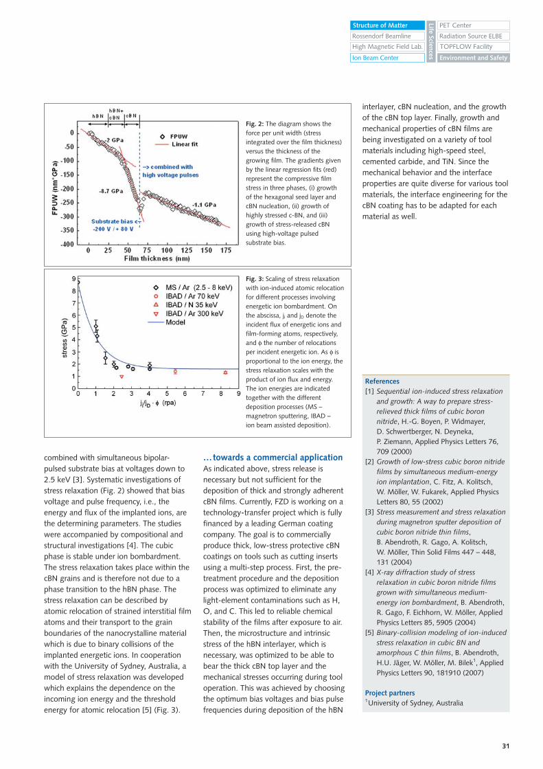
31
combined with simultaneous bipolar-pulsed substrate bias at voltages down to2.5 keV [3]. Systematic investigations ofstress relaxation (Fig. 2) showed that biasvoltage and pulse frequency, i.e., theenergy and flux of the implanted ions, arethe determining parameters. The studieswere accompanied by compositional andstructural investigations [4]. The cubicphase is stable under ion bombardment.The stress relaxation takes place within thecBN grains and is therefore not due to aphase transition to the hBN phase. Thestress relaxation can be described byatomic relocation of strained interstitial filmatoms and their transport to the grainboundaries of the nanocrystalline materialwhich is due to binary collisions of theimplanted energetic ions. In cooperationwith the University of Sydney, Australia, amodel of stress relaxation was developedwhich explains the dependence on theincoming ion energy and the thresholdenergy for atomic relocation [5] (Fig. 3).
…towards a commercial applicationAs indicated above, stress release isnecessary but not sufficient for thedeposition of thick and strongly adherentcBN films. Currently, FZD is working on atechnology-transfer project which is fullyfinanced by a leading German coatingcompany. The goal is to commerciallyproduce thick, low-stress protective cBNcoatings on tools such as cutting insertsusing a multi-step process. First, the pre-treatment procedure and the depositionprocess was optimized to eliminate anylight-element contaminations such as H,O, and C. This led to reliable chemicalstability of the films after exposure to air.Then, the microstructure and intrinsicstress of the hBN interlayer, which isnecessary, was optimized to be able tobear the thick cBN top layer and themechanical stresses occurring during tooloperation. This was achieved by choosingthe optimum bias voltages and bias pulsefrequencies during deposition of the hBN
interlayer, cBN nucleation, and the growthof the cBN top layer. Finally, growth andmechanical properties of cBN films arebeing investigated on a variety of toolmaterials including high-speed steel,cemented carbide, and TiN. Since themechanical behavior and the interfaceproperties are quite diverse for various toolmaterials, the interface engineering for thecBN coating has to be adapted for eachmaterial as well.
References[1] Sequential ion-induced stress relaxation
and growth: A way to prepare stress-relieved thick films of cubic boron nitride, H.-G. Boyen, P. Widmayer, D. Schwertberger, N. Deyneka, P. Ziemann, Applied Physics Letters 76, 709 (2000)
[2] Growth of low-stress cubic boron nitride films by simultaneous medium-energy ion implantation, C. Fitz, A. Kolitsch, W. Möller, W. Fukarek, Applied Physics Letters 80, 55 (2002)
[3] Stress measurement and stress relaxation during magnetron sputter deposition of cubic boron nitride thin films, B. Abendroth, R. Gago, A. Kolitsch, W. Möller, Thin Solid Films 447 – 448, 131 (2004)
[4] X-ray diffraction study of stress relaxation in cubic boron nitride films grown with simultaneous medium-energy ion bombardment, B. Abendroth, R. Gago, F. Eichhorn, W. Möller, Applied Physics Letters 85, 5905 (2004)
[5] Binary-collision modeling of ion-induced stress relaxation in cubic BN and amorphous C thin films, B. Abendroth, H.U. Jäger, W. Möller, M. Bilek1, Applied Physics Letters 90, 181910 (2007)
Project partners1University of Sydney, Australia
Fig. 2: The diagram shows theforce per unit width (stressintegrated over the film thickness)versus the thickness of thegrowing film. The gradients givenby the linear regression fits (red)represent the compressive filmstress in three phases, (i) growthof the hexagonal seed layer andcBN nucleation, (ii) growth ofhighly stressed c-BN, and (iii)growth of stress-released cBNusing high-voltage pulsedsubstrate bias.
Rossendorf Beamline
Environment and Safety
Structure of Matter
Life Sciences
TOPFLOW FacilityHigh Magnetic Field Lab.
PET Center
Ion Beam Center
Radiation Source ELBE
Fig. 3: Scaling of stress relaxationwith ion-induced atomic relocationfor different processes involvingenergetic ion bombardment. Onthe abscissa, ji and jD denote theincident flux of energetic ions andfilm-forming atoms, respectively,and φ the number of relocationsper incident energetic ion. As φ isproportional to the ion energy, thestress relaxation scales with theproduct of ion flux and energy.The ion energies are indicatedtogether with the differentdeposition processes (MS –magnetron sputtering, IBAD – ion beam assisted deposition).
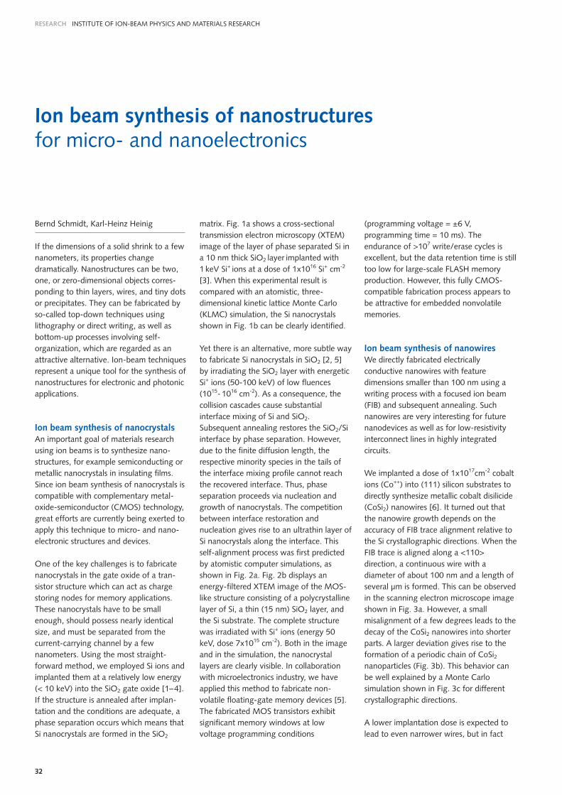
RESEARCH INSTITUTE OF ION-BEAM PHYSICS AND MATERIALS RESEARCH
32
Bernd Schmidt, Karl-Heinz Heinig
If the dimensions of a solid shrink to a fewnanometers, its properties changedramatically. Nanostructures can be two,one, or zero-dimensional objects corres-ponding to thin layers, wires, and tiny dotsor precipitates. They can be fabricated byso-called top-down techniques usinglithography or direct writing, as well asbottom-up processes involving self-organization, which are regarded as anattractive alternative. Ion-beam techniquesrepresent a unique tool for the synthesis ofnanostructures for electronic and photonicapplications.
Ion beam synthesis of nanocrystalsAn important goal of materials researchusing ion beams is to synthesize nano-structures, for example semiconducting ormetallic nanocrystals in insulating films.Since ion beam synthesis of nanocrystals iscompatible with complementary metal-oxide-semiconductor (CMOS) technology,great efforts are currently being exerted toapply this technique to micro- and nano-electronic structures and devices.
One of the key challenges is to fabricatenanocrystals in the gate oxide of a tran-sistor structure which can act as chargestoring nodes for memory applications.These nanocrystals have to be smallenough, should possess nearly identicalsize, and must be separated from thecurrent-carrying channel by a fewnanometers. Using the most straight-forward method, we employed Si ions andimplanted them at a relatively low energy(< 10 keV) into the SiO2 gate oxide [1–4].If the structure is annealed after implan-tation and the conditions are adequate, aphase separation occurs which means thatSi nanocrystals are formed in the SiO2
matrix. Fig. 1a shows a cross-sectionaltransmission electron microscopy (XTEM)image of the layer of phase separated Si ina 10 nm thick SiO2 layer implanted with1 keV Si+ ions at a dose of 1x10¹⁶ Si+ cm-2
[3]. When this experimental result iscompared with an atomistic, three-dimensional kinetic lattice Monte Carlo(KLMC) simulation, the Si nanocrystalsshown in Fig. 1b can be clearly identified.
Yet there is an alternative, more subtle wayto fabricate Si nanocrystals in SiO2 [2, 5]by irradiating the SiO2 layer with energeticSi+ ions (50-100 keV) of low fluences(1015- 1016 cm-2). As a consequence, thecollision cascades cause substantialinterface mixing of Si and SiO2.Subsequent annealing restores the SiO2/Siinterface by phase separation. However,due to the finite diffusion length, therespective minority species in the tails ofthe interface mixing profile cannot reachthe recovered interface. Thus, phaseseparation proceeds via nucleation andgrowth of nanocrystals. The competitionbetween interface restoration andnucleation gives rise to an ultrathin layer ofSi nanocrystals along the interface. Thisself-alignment process was first predictedby atomistic computer simulations, asshown in Fig. 2a. Fig. 2b displays anenergy-filtered XTEM image of the MOS-like structure consisting of a polycrystallinelayer of Si, a thin (15 nm) SiO2 layer, andthe Si substrate. The complete structurewas irradiated with Si+ ions (energy 50keV, dose 7x1015 cm-2). Both in the imageand in the simulation, the nanocrystallayers are clearly visible. In collaborationwith microelectronics industry, we haveapplied this method to fabricate non-volatile floating-gate memory devices [5].The fabricated MOS transistors exhibitsignificant memory windows at lowvoltage programming conditions
(programming voltage = ±6 V,programming time = 10 ms). Theendurance of >107 write/erase cycles isexcellent, but the data retention time is stilltoo low for large-scale FLASH memoryproduction. However, this fully CMOS-compatible fabrication process appears tobe attractive for embedded nonvolatilememories.
Ion beam synthesis of nanowiresWe directly fabricated electricallyconductive nanowires with featuredimensions smaller than 100 nm using awriting process with a focused ion beam(FIB) and subsequent annealing. Suchnanowires are very interesting for futurenanodevices as well as for low-resistivityinterconnect lines in highly integratedcircuits.
We implanted a dose of 1x1017cm-2 cobaltions (Co++) into (111) silicon substrates todirectly synthesize metallic cobalt disilicide(CoSi2) nanowires [6]. It turned out thatthe nanowire growth depends on theaccuracy of FIB trace alignment relative tothe Si crystallographic directions. When theFIB trace is aligned along a <110>direction, a continuous wire with adiameter of about 100 nm and a length ofseveral µm is formed. This can be observedin the scanning electron microscope imageshown in Fig. 3a. However, a smallmisalignment of a few degrees leads to thedecay of the CoSi2 nanowires into shorterparts. A larger deviation gives rise to theformation of a periodic chain of CoSi2nanoparticles (Fig. 3b). This behavior canbe well explained by a Monte Carlosimulation shown in Fig. 3c for differentcrystallographic directions.
A lower implantation dose is expected tolead to even narrower wires, but in fact
Ion beam synthesis of nanostructuresfor micro- and nanoelectronics
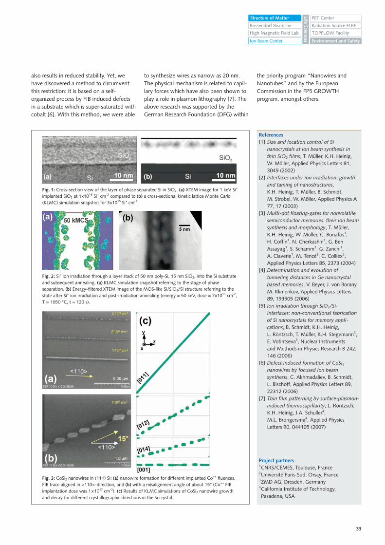
33
also results in reduced stability. Yet, wehave discovered a method to circumventthis restriction: it is based on a self-organized process by FIB induced defectsin a substrate which is super-saturated withcobalt [6]. With this method, we were able
to synthesize wires as narrow as 20 nm.The physical mechanism is related to capil-lary forces which have also been shown toplay a role in plasmon lithography [7]. Theabove research was supported by theGerman Research Foundation (DFG) within
the priority program “Nanowires andNanotubes” and by the EuropeanCommission in the FP5 GROWTHprogram, amongst others.
Fig. 3: CoSi2 nanowires in (111) Si: (a) nanowire formation for different implanted Co++ fluences,FIB trace aligned in <110>-direction, and (b) with a misalignment angle of about 15° (Co++ FIBimplantation dose was 1x1017 cm-2). (c) Results of KLMC simulations of CoSi2 nanowire growthand decay for different crystallographic directions in the Si crystal.
Fig. 1: Cross-section view of the layer of phase separated Si in SiO2. (a) XTEM image for 1 keV Si+
implanted SiO2 at 1x10¹⁶ Si+ cm-2 compared to (b) a cross-sectional kinetic lattice Monte Carlo(KLMC) simulation snapshot for 3x10¹⁵ Si+ cm-2.
References[1] Size and location control of Si
nanocrystals at ion beam synthesis in thin SiO2 films, T. Müller, K.H. Heinig, W. Möller, Applied Physics Letters 81, 3049 (2002)
[2] Interfaces under ion irradiation: growth and taming of nanostructures, K.H. Heinig, T. Müller, B. Schmidt, M. Strobel, W. Möller, Applied Physics A 77, 17 (2003)
[3] Multi-dot floating-gates for nonvolatile semiconductor memories: their ion beam synthesis and morphology, T. Müller, K.H. Heinig, W. Möller, C. Bonafos1, H. Coffin1, N. Cherkashin1, G. Ben Assayag1, S. Schamm1, G. Zanchi1, A. Claverie1, M. Tencé2, C. Colliex2, Applied Physics Letters 85, 2373 (2004)
[4] Determination and evolution of tunneling distances in Ge nanocrystal based memories, V. Beyer, J. von Borany, M. Klimenkov, Applied Physics Letters 89, 193505 (2006)
[5] Ion irradiation through SiO2/Si-interfaces: non-conventional fabrication of Si nanocrystals for memory appli-cations, B. Schmidt, K.H. Heinig, L. Röntzsch, T. Müller, K.H. Stegemann3, E. Votintseva3, Nuclear Instruments and Methods in Physics Research B 242, 146 (2006)
[6] Defect induced formation of CoSi2nanowires by focused ion beam synthesis, C. Akhmadaliev, B. Schmidt, L. Bischoff, Applied Physics Letters 89, 22312 (2006)
[7] Thin film patterning by surface-plasmon-induced thermocapillarity, L. Röntzsch, K.H. Heinig, J.A. Schuller4, M.L. Brongersma4, Applied Physics Letters 90, 044105 (2007)
Project partners1CNRS/CEMES, Toulouse, France2Université Paris-Sud, Orsay, France3ZMD AG, Dresden, Germany4California Institute of Technology, Pasadena, USA
Rossendorf Beamline
Environment and Safety
Structure of Matter
Life Sciences
TOPFLOW FacilityHigh Magnetic Field Lab.
PET Center
Ion Beam Center
Radiation Source ELBE
Fig. 2: Si+ ion irradiation through a layer stack of 50 nm poly-Si, 15 nm SiO2, into the Si substrateand subsequent annealing. (a) KLMC simulation snapshot referring to the stage of phaseseparation. (b) Energy-filtered XTEM image of the MOS-like Si/SiO2/Si structure referring to thestate after Si+ ion irradiation and post-irradiation annealing (energy = 50 keV, dose = 7x1015 cm-2,T = 1050 °C, t = 120 s).
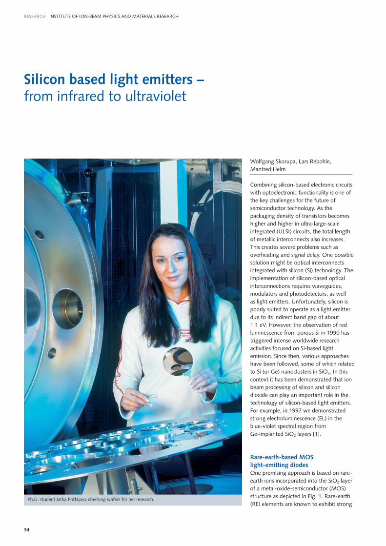
RESEARCH INSTITUTE OF ION-BEAM PHYSICS AND MATERIALS RESEARCH
34
Wolfgang Skorupa, Lars Rebohle, Manfred Helm
Combining silicon-based electronic circuitswith optoelectronic functionality is one ofthe key challenges for the future ofsemiconductor technology. As thepackaging density of transistors becomeshigher and higher in ultra-large-scaleintegrated (ULSI) circuits, the total lengthof metallic interconnects also increases.This creates severe problems such asoverheating and signal delay. One possiblesolution might be optical interconnectsintegrated with silicon (Si) technology. Theimplementation of silicon-based opticalinterconnections requires waveguides,modulators and photodetectors, as well as light emitters. Unfortunately, silicon ispoorly suited to operate as a light emitterdue to its indirect band gap of about 1.1 eV. However, the observation of redluminescence from porous Si in 1990 hastriggered intense worldwide researchactivities focused on Si-based lightemission. Since then, various approacheshave been followed, some of which relatedto Si (or Ge) nanoclusters in SiO2. In thiscontext it has been demonstrated that ionbeam processing of silicon and silicondioxide can play an important role in thetechnology of silicon-based light emitters.For example, in 1997 we demonstratedstrong electroluminescence (EL) in theblue-violet spectral region from Ge-implanted SiO2 layers [1].
Rare-earth-based MOS light-emitting diodesOne promising approach is based on rare-earth ions incorporated into the SiO2 layerof a metal-oxide-semiconductor (MOS)structure as depicted in Fig. 1. Rare-earth(RE) elements are known to exhibit strong
Silicon based light emitters – from infrared to ultraviolet
Ph.D. student Jarka Potfajova checking wafers for her research.
35
and sharp luminescence lines related totransitions between levels within theunfilled 4f shell. The most famous andwidely used example is trivalent erbium(Er3+), which is commonly employed forfiber amplifiers operating in thetelecommunication band at 1.54 µm.Other RE ions, due to their differentenergy level structure, can generatedifferent wavelengths throughout thespectrum from the infrared (IR) to the
ultraviolet (UV). These ions can beconveniently incorporated into the SiO2
matrix by means of ion implantation.When applying a bias between the gateand the substrate of the MOS structure,the RE ions are impact-excited by hotelectrons, which are accelerated in the SiO2
conduction band by the high electric fieldafter Fowler-Nordheim tunneling throughthe oxide barrier.
In Fig. 2, electroluminescence spectra ofMOS devices doped with different rare-earth elements are shown. Emitterstructures doped with gadolinium (Gd, toppanel) are quite remarkable since theyexhibit a single, sharp emission line at a UVwavelength as short as 316 nm [2]. Thisspectral range cannot be reached easily byother semiconductor devices and may berelevant for exciting fluorescence inbiosensing applications.
Terbium (Tb), which emits intense greenlight mainly at a wavelength of 541 nm[3], is the element among the rare earthswith the highest external quantumefficiency of up to 15 %. Since thiswavelength also matches the peaksensitivity of the human eye it could beapplied for micro-displays. We alsoinvestigated the interaction of different REelements implanted in the same oxidelayer. If the emission band of one elementmatches the absorption band of the other,the EL intensity of the latter can bestrongly increased. This is caused by aresonant energy transfer from one rareearth to the other. This phenomenon wasdemonstrated with cerium (Ce) implantedlayers co-doped with Gd, where theexcited Gd ions transfer their energy to theCe ions [4]. The spectrum of a Ce-dopedSiO2 structure is also shown in Fig. 2,where the broad blue emission band isimmediately noticeable. This stands incontrast to the sharp emission lines of theother RE elements. This is owed to the factthat the blue Ce luminescence does notderive from a 4f intra-shell but rather froman inter-configurational 5d-4f transition.
A very interesting phenomenon isobserved with europium (Eu)-dopedstructures. While most rare earths occur inthe RE3+ oxidation state when incorporatedinto a matrix, Eu exists in both the Eu3+
and Eu2+ state. While the former shows ared intra-4f luminescence, the latter givesrise to blue 5d-4f emission. Both areobserved in our EL spectrum as seen in thebottom panel of Fig. 2. We have recentlyshown that the relative strength of theemission bands, and thus the color of theemitted light, changes with the excitationcurrent. Hence, we have constructed aswitchable multi-color light emitter [5].
Fig. 1: Scheme of a rare-earth-doped MOS light-emitting structure.
Fig. 2: Electroluminescence spectrafrom various rare-earth-implantedMOS devices. The transitions of themain emission lines are given in thediagrams.
Rossendorf Beamline
Environment and Safety
Structure of Matter
Life Sciences
TOPFLOW FacilityHigh Magnetic Field Lab.
PET Center
Ion Beam Center
Radiation Source ELBE
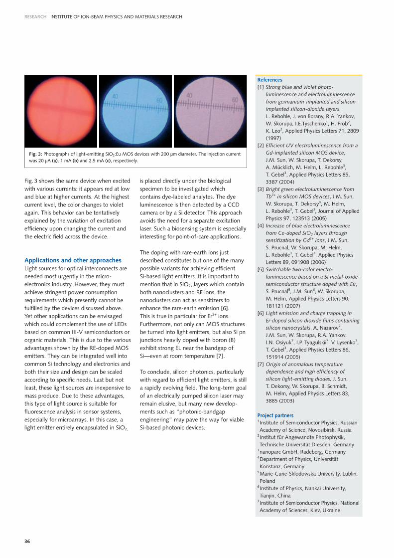
RESEARCH INSTITUTE OF ION-BEAM PHYSICS AND MATERIALS RESEARCH
36
Fig. 3 shows the same device when excitedwith various currents: it appears red at lowand blue at higher currents. At the highestcurrent level, the color changes to violetagain. This behavior can be tentativelyexplained by the variation of excitationefficiency upon changing the current andthe electric field across the device.
Applications and other approachesLight sources for optical interconnects areneeded most urgently in the micro-electronics industry. However, they mustachieve stringent power consumptionrequirements which presently cannot befulfilled by the devices discussed above.Yet other applications can be envisagedwhich could complement the use of LEDsbased on common III-V semiconductors ororganic materials. This is due to the variousadvantages shown by the RE-doped MOSemitters. They can be integrated well intocommon Si technology and electronics andboth their size and design can be scaledaccording to specific needs. Last but notleast, these light sources are inexpensive tomass produce. Due to these advantages,this type of light source is suitable forfluorescence analysis in sensor systems,especially for microarrays. In this case, alight emitter entirely encapsulated in SiO2,
is placed directly under the biologicalspecimen to be investigated whichcontains dye-labeled analytes. The dyeluminescence is then detected by a CCDcamera or by a Si detector. This approachavoids the need for a separate excitationlaser. Such a biosensing system is especiallyinteresting for point-of-care applications.
The doping with rare-earth ions justdescribed constitutes but one of the manypossible variants for achieving efficient Si-based light emitters. It is important tomention that in SiO2, layers which containboth nanoclusters and RE ions, thenanoclusters can act as sensitizers toenhance the rare-earth emission [6]. This is true in particular for Er3+ ions.Furthermore, not only can MOS structuresbe turned into light emitters, but also Si pnjunctions heavily doped with boron (B)exhibit strong EL near the bandgap of Si—even at room temperature [7].
To conclude, silicon photonics, particularlywith regard to efficient light emitters, is stilla rapidly evolving field. The long-term goalof an electrically pumped silicon laser mayremain elusive, but many new develop-ments such as “photonic-bandgapengineering” may pave the way for viableSi-based photonic devices.
Fig. 3: Photographs of light-emitting SiO2:Eu MOS devices with 200 µm diameter. The injection currentwas 20 µA (a), 1 mA (b) and 2.5 mA (c), respectively.
References[1] Strong blue and violet photo-
luminescence and electroluminescence from germanium-implanted and silicon-implanted silicon-dioxide layers, L. Rebohle, J. von Borany, R.A. Yankov, W. Skorupa, I.E.Tyschenko1, H. Fröb2, K. Leo2, Applied Physics Letters 71, 2809 (1997)
[2] Efficient UV electroluminescence from a Gd-implanted silicon MOS device, J.M. Sun, W. Skorupa, T. Dekorsy, A. Mücklich, M. Helm, L. Rebohle3, T. Gebel3, Applied Physics Letters 85, 3387 (2004)
[3] Bright green electroluminescence from Tb3+ in silicon MOS devices, J.M. Sun, W. Skorupa, T. Dekorsy4, M. Helm, L. Rebohle3, T. Gebel3, Journal of Applied Physics 97, 123513 (2005)
[4] Increase of blue electroluminescence from Ce-doped SiO2 layers through sensitization by Gd3+ ions, J.M. Sun, S. Prucnal, W. Skorupa, M. Helm, L. Rebohle3, T. Gebel3, Applied Physics Letters 89, 091908 (2006)
[5] Switchable two-color electro-luminescence based on a Si metal-oxide-semiconductor structure doped with Eu, S. Prucnal5, J.M. Sun6, W. Skorupa, M. Helm, Applied Physics Letters 90, 181121 (2007)
[6] Light emission and charge trapping in Er-doped silicon dioxide films containing silicon nanocrystals, A. Nazarov7, J.M. Sun, W. Skorupa, R.A. Yankov, I.N. Osiyuk7, I.P. Tyagulskii7, V. Lysenko7, T. Gebel3, Applied Physics Letters 86, 151914 (2005)
[7] Origin of anomalous temperature dependence and high efficiency of silicon light-emitting diodes, J. Sun, T. Dekorsy, W. Skorupa, B. Schmidt, M. Helm, Applied Physics Letters 83, 3885 (2003)
Project partners1Institute of Semiconductor Physics, Russian Academy of Science, Novosibirsk, Russia
2Institut für Angewandte Photophysik, Technische Universität Dresden, Germany
3nanoparc GmbH, Radeberg, Germany4Department of Physics, Universität Konstanz, Germany
5Marie-Curie-Sklodowska University, Lublin, Poland
6Institute of Physics, Nankai University, Tianjin, China
7Institute of Semiconductor Physics, National Academy of Sciences, Kiev, Ukraine
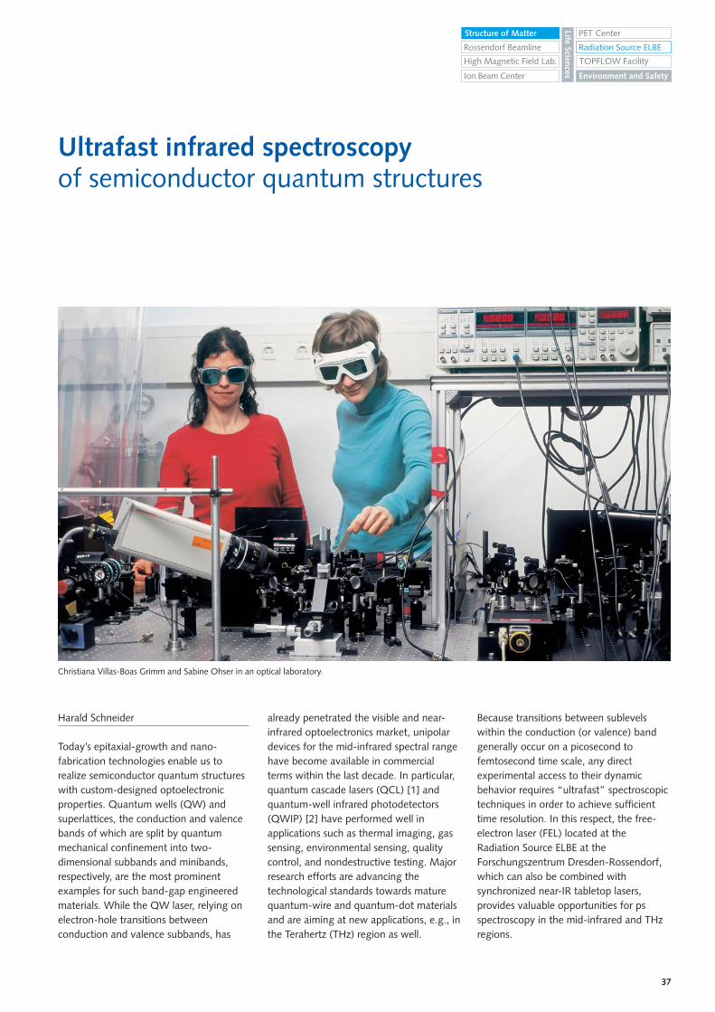
37
Harald Schneider
Today’s epitaxial-growth and nano-fabrication technologies enable us torealize semiconductor quantum structureswith custom-designed optoelectronicproperties. Quantum wells (QW) andsuperlattices, the conduction and valencebands of which are split by quantummechanical confinement into two-dimensional subbands and minibands,respectively, are the most prominentexamples for such band-gap engineeredmaterials. While the QW laser, relying onelectron-hole transitions betweenconduction and valence subbands, has
already penetrated the visible and near-infrared optoelectronics market, unipolardevices for the mid-infrared spectral rangehave become available in commercialterms within the last decade. In particular,quantum cascade lasers (QCL) [1] andquantum-well infrared photodetectors(QWIP) [2] have performed well inapplications such as thermal imaging, gassensing, environmental sensing, qualitycontrol, and nondestructive testing. Majorresearch efforts are advancing thetechnological standards towards maturequantum-wire and quantum-dot materialsand are aiming at new applications, e.g., inthe Terahertz (THz) region as well.
Because transitions between sublevelswithin the conduction (or valence) bandgenerally occur on a picosecond tofemtosecond time scale, any directexperimental access to their dynamicbehavior requires “ultrafast” spectroscopictechniques in order to achieve sufficienttime resolution. In this respect, the free-electron laser (FEL) located at theRadiation Source ELBE at theForschungszentrum Dresden-Rossendorf,which can also be combined withsynchronized near-IR tabletop lasers,provides valuable opportunities for psspectroscopy in the mid-infrared and THzregions.
Ultrafast infrared spectroscopy of semiconductor quantum structures
Christiana Villas-Boas Grimm and Sabine Ohser in an optical laboratory.
Rossendorf Beamline
Environment and Safety
Structure of Matter
Life Sciences
TOPFLOW FacilityHigh Magnetic Field Lab.
PET Center
Ion Beam Center
Radiation Source ELBE
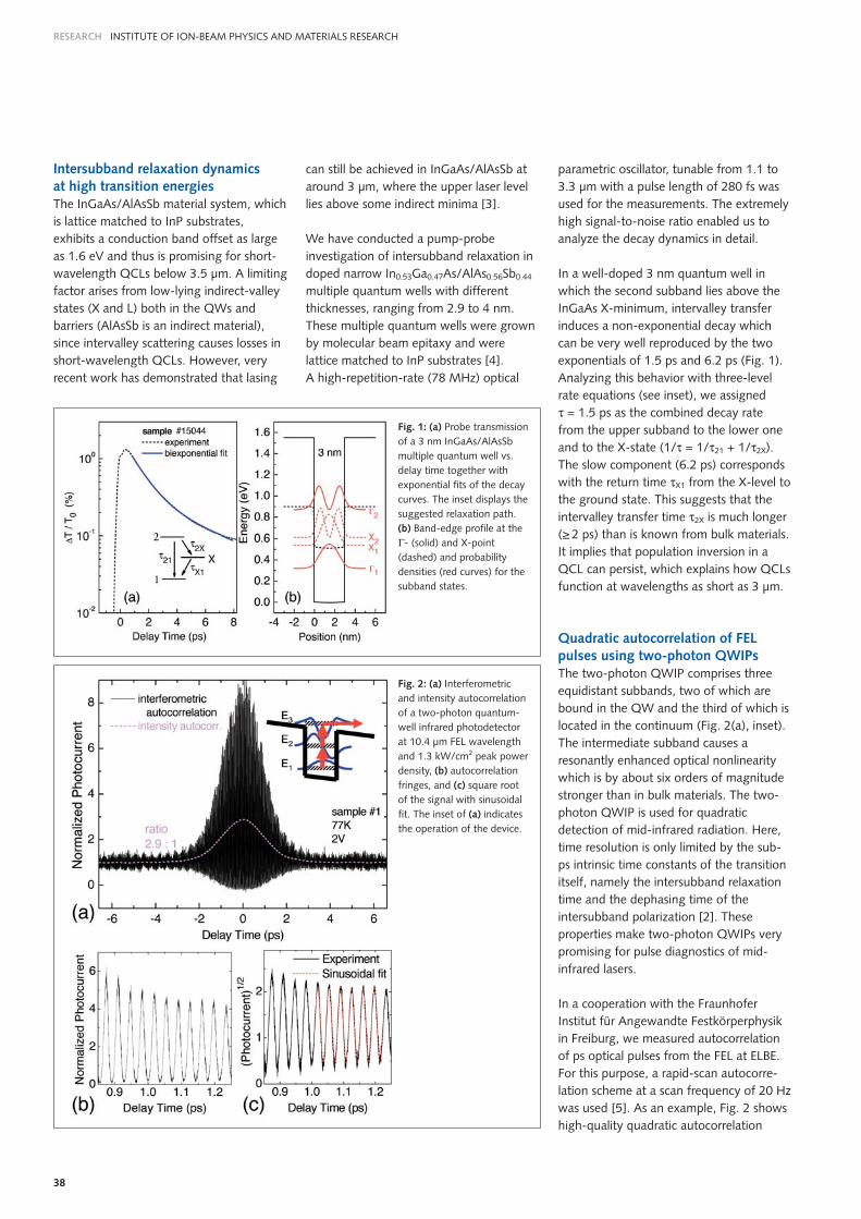
RESEARCH INSTITUTE OF ION-BEAM PHYSICS AND MATERIALS RESEARCH
38
Intersubband relaxation dynamics at high transition energiesThe InGaAs/AlAsSb material system, whichis lattice matched to InP substrates,exhibits a conduction band offset as largeas 1.6 eV and thus is promising for short-wavelength QCLs below 3.5 µm. A limitingfactor arises from low-lying indirect-valleystates (X and L) both in the QWs andbarriers (AlAsSb is an indirect material),since intervalley scattering causes losses inshort-wavelength QCLs. However, veryrecent work has demonstrated that lasing
can still be achieved in InGaAs/AlAsSb ataround 3 µm, where the upper laser levellies above some indirect minima [3].
We have conducted a pump-probeinvestigation of intersubband relaxation indoped narrow In0.53Ga0.47As/AlAs0.56Sb0.44
multiple quantum wells with differentthicknesses, ranging from 2.9 to 4 nm.These multiple quantum wells were grownby molecular beam epitaxy and werelattice matched to InP substrates [4]. A high-repetition-rate (78 MHz) optical
parametric oscillator, tunable from 1.1 to3.3 µm with a pulse length of 280 fs wasused for the measurements. The extremelyhigh signal-to-noise ratio enabled us toanalyze the decay dynamics in detail.
In a well-doped 3 nm quantum well inwhich the second subband lies above theInGaAs X-minimum, intervalley transferinduces a non-exponential decay whichcan be very well reproduced by the twoexponentials of 1.5 ps and 6.2 ps (Fig. 1).Analyzing this behavior with three-levelrate equations (see inset), we assigned τ = 1.5 ps as the combined decay ratefrom the upper subband to the lower oneand to the X-state (1/τ = 1/τ21 + 1/τ2X).The slow component (6.2 ps) correspondswith the return time τX1 from the X-level tothe ground state. This suggests that theintervalley transfer time τ2X is much longer(≥ 2 ps) than is known from bulk materials.It implies that population inversion in aQCL can persist, which explains how QCLsfunction at wavelengths as short as 3 µm.
Quadratic autocorrelation of FELpulses using two-photon QWIPs The two-photon QWIP comprises threeequidistant subbands, two of which arebound in the QW and the third of which islocated in the continuum (Fig. 2(a), inset).The intermediate subband causes aresonantly enhanced optical nonlinearitywhich is by about six orders of magnitudestronger than in bulk materials. The two-photon QWIP is used for quadraticdetection of mid-infrared radiation. Here,time resolution is only limited by the sub-ps intrinsic time constants of the transitionitself, namely the intersubband relaxationtime and the dephasing time of theintersubband polarization [2]. Theseproperties make two-photon QWIPs verypromising for pulse diagnostics of mid-infrared lasers.
In a cooperation with the FraunhoferInstitut für Angewandte Festkörperphysikin Freiburg, we measured autocorrelationof ps optical pulses from the FEL at ELBE.For this purpose, a rapid-scan autocorre-lation scheme at a scan frequency of 20 Hzwas used [5]. As an example, Fig. 2 showshigh-quality quadratic autocorrelation
Fig. 1: (a) Probe transmissionof a 3 nm InGaAs/AlAsSbmultiple quantum well vs.delay time together withexponential fits of the decaycurves. The inset displays thesuggested relaxation path.(b) Band-edge profile at theΓ- (solid) and X-point(dashed) and probabilitydensities (red curves) for thesubband states.
Fig. 2: (a) Interferometricand intensity autocorrelationof a two-photon quantum-well infrared photodetectorat 10.4 µm FEL wavelengthand 1.3 kW/cm2 peak powerdensity, (b) autocorrelationfringes, and (c) square rootof the signal with sinusoidalfit. The inset of (a) indicatesthe operation of the device.
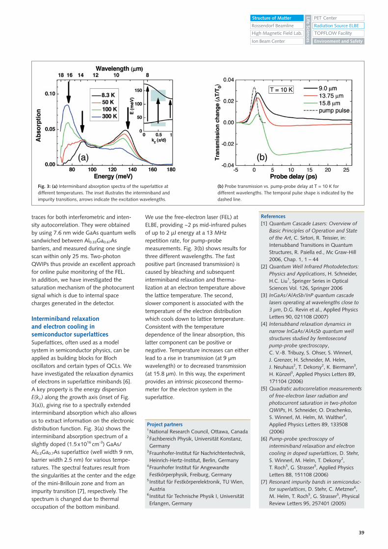
39
traces for both interferometric and inten-sity autocorrelation. They were obtainedby using 7.6 nm wide GaAs quantum wellssandwiched between Al0.33Ga0.67Asbarriers, and measured during one singlescan within only 25 ms. Two-photonQWIPs thus provide an excellent approachfor online pulse monitoring of the FEL. In addition, we have investigated thesaturation mechanism of the photocurrentsignal which is due to internal spacecharges generated in the detector.
Interminiband relaxation and electron cooling insemiconductor superlattices Superlattices, often used as a modelsystem in semiconductor physics, can beapplied as building blocks for Blochoscillators and certain types of QCLs. Wehave investigated the relaxation dynamicsof electrons in superlattice minibands [6].A key property is the energy dispersionE(kz) along the growth axis (inset of Fig.3(a)), giving rise to a spectrally extendedinterminiband absorption which also allowsus to extract information on the electronicdistribution function. Fig. 3(a) shows theinterminiband absorption spectrum of aslightly doped (1.5x1016 cm-3) GaAs/Al0.3Ga0.7As superlattice (well width 9 nm,barrier width 2.5 nm) for various tempe-ratures. The spectral features result fromthe singularities at the center and the edgeof the mini-Brillouin zone and from animpurity transition [7], respectively. Thespectrum is changed due to thermaloccupation of the bottom miniband.
We use the free-electron laser (FEL) atELBE, providing ~2 ps mid-infrared pulsesof up to 2 µJ energy at a 13 MHzrepetition rate, for pump-probemeasurements. Fig. 3(b) shows results forthree different wavelengths. The fastpositive part (increased transmission) iscaused by bleaching and subsequentinterminiband relaxation and therma-lization at an electron temperature abovethe lattice temperature. The second, slower component is associated with thetemperature of the electron distributionwhich cools down to lattice temperature.Consistent with the temperaturedependence of the linear absorption, thislatter component can be positive ornegative. Temperature increases can eitherlead to a rise in transmission (at 9 µmwavelength) or to decreased transmission(at 15.8 µm). In this way, the experimentprovides an intrinsic picosecond thermo-meter for the electron system in thesuperlattice.
Fig. 3: (a) Interminiband absorption spectra of the superlattice atdifferent temperatures. The inset illustrates the interminiband andimpurity transitions, arrows indicate the excitation wavelengths.
(b) Probe transmission vs. pump-probe delay at T = 10 K fordifferent wavelengths. The temporal pulse shape is indicated by thedashed line.
Project partners1National Research Council, Ottawa, Canada2Fachbereich Physik, Universität Konstanz, Germany
3Fraunhofer-Institut für Nachrichtentechnik, Heinrich-Hertz-Institut, Berlin, Germany
4Fraunhofer Institut für Angewandte Festkörperphysik, Freiburg, Germany
5Institut für Festkörperelektronik, TU Wien, Austria
6 Institut für Technische Physik I, Universität Erlangen, Germany
References[1] Quantum Cascade Lasers: Overview of
Basic Principles of Operation and State of the Art, C. Sirtori, R. Teissier, in: Intersubband Transitions in Quantum Structures, R. Paiella ed., Mc Graw-Hill 2006, Chap. 1, 1 – 44
[2] Quantum Well Infrared Photodetectors: Physics and Applications, H. Schneider, H.C. Liu1, Springer Series in Optical Sciences Vol. 126, Springer 2006
[3] InGaAs/AlAsSb/InP quantum cascade lasers operating at wavelengths close to 3 µm, D.G. Revin et al., Applied Physics Letters 90, 021108 (2007)
[4] Intersubband relaxation dynamics in narrow InGaAs/AlAsSb quantum well structures studied by femtosecond pump-probe spectroscopy, C. V.-B. Tribuzy, S. Ohser, S. Winnerl, J. Grenzer, H. Schneider, M. Helm, J. Neuhaus2, T. Dekorsy2, K. Biermann3, H. Künzel3, Applied Physics Letters 89, 171104 (2006)
[5] Quadratic autocorrelation measurements of free-electron laser radiation and photocurrent saturation in two-photon QWIPs, H. Schneider, O. Drachenko, S. Winnerl, M. Helm, M. Walther4, Applied Physics Letters 89, 133508 (2006)
[6] Pump-probe spectroscopy of interminiband relaxation and electron cooling in doped superlattices, D. Stehr, S. Winnerl, M. Helm, T. Dekorsy2, T. Roch5, G. Strasser5, Applied Physics Letters 88, 151108 (2006)
[7] Resonant impurity bands in semiconduc-tor superlattices, D. Stehr, C. Metzner6, M. Helm, T. Roch5, G. Strasser5, Physical Review Letters 95, 257401 (2005)
Rossendorf Beamline
Environment and Safety
Structure of Matter
Life Sciences
TOPFLOW FacilityHigh Magnetic Field Lab.
PET Center
Ion Beam Center
Radiation Source ELBE
40
FACTS & FIGURES
41
The Forschungszentrum Dresden-Rossendorf (FZD) is a multi-disciplinary research centerfor natural sciences and technology. It is the largest institute of the Leibniz Associationand is equally funded by the Federal Republic of Germany and the Federal States, inparticular by the Free State of Saxony. At the FZD, around 225 scientists are engaged inthree different research programs of basic and application-oriented research. Scientistsworking in the Structure of Matter program investigate the reactions of matter wheninfluenced by high fields and minuscule dimensions. Research and development in theLife Sciences program is focused on the imaging of tumors and the effective radiationtreatment of cancer. How can humankind and the environment be protected fromtechnical risks? – This question is in the center of research in the Environment and Safetyprogram of the FZD.
In the following Facts & Figures section data presenting the scientific output in theStructure of Matter research program are given as well as information on staff andfunding at the FZD.
Facts & Figures

42
2004 2005 2006
Research Programs
Structure of Matter
Life Sciences
Environment and Safety
Facilities
Sum
Public FundingT€
13.858
8.241
13.005
20.721
55.825
Project FundingT€
1.190
801
3.180
911
6.082
Public FundingT€
14.209
6.266
12.950
20.428
53.853
Project FundingT€
1.259
645
3.656
756
6.316
Public FundingT€
19.575
8.191
11.866
17.988
57.620
Project FundingT€
1.405
784
3.990
1.643
7.822
Structure of Matter Life Sciences Environment and Safety
10
8
6
4
2
02004 2005 2006
250
200
150
100
50
02004 2005 2006
Patents
Publications
staff scientists third-party funded scientistsguest scientists postdocs
50
40
30
20
10
02004 2005 2006
Scientific staff
Budget
This figure shows the number of applications for a patent filed in eachresearch program of the FZD during the last years. National andinternational applications for a patent of one and the same inventionare only counted once.
This chart displays the evolution of peer-reviewed articles by scientistsfrom the FZD’s Structure of Matter program.
This table displays the share of each research program as well as the experimental facilities located at the FZD of both public and projectfunding during the last three years.
This chart shows the evolution of posts occupied by scientificpersonnel in the Structure of Matter program of the FZD. Third-party funded scientists, guest scientists, and postdocsrepresented by the corresponding figures are given in units ofpaid full-time posts.
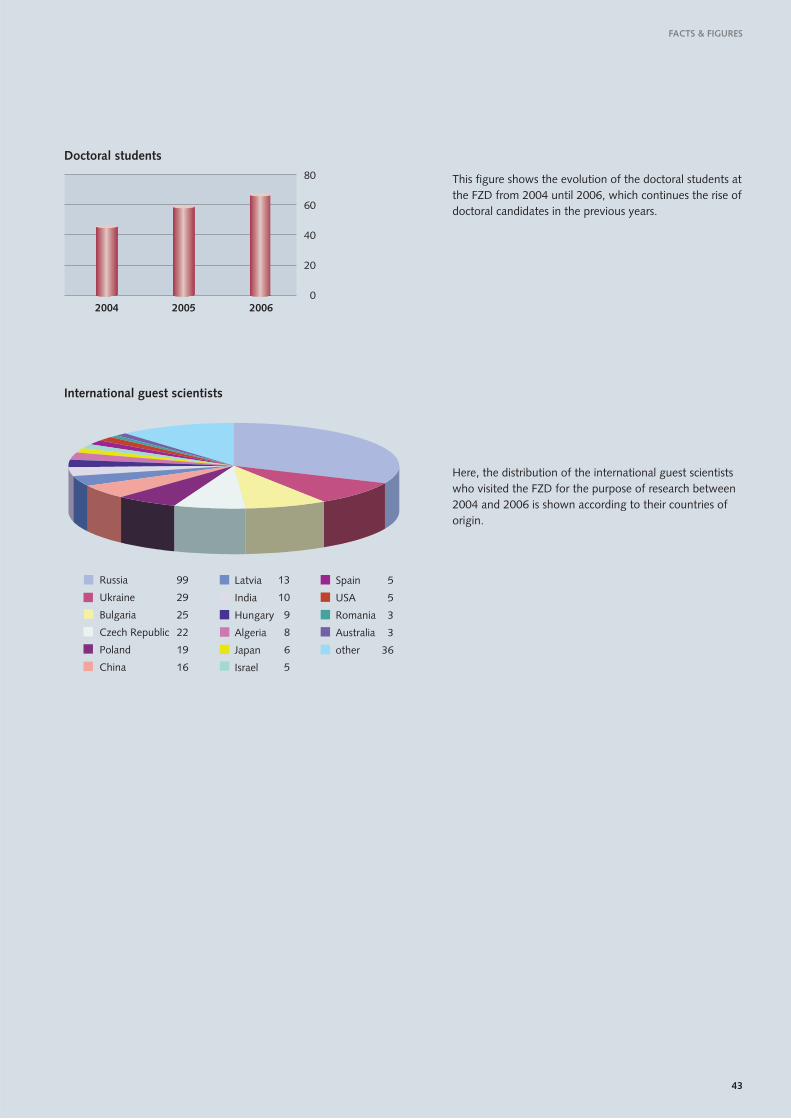
FACTS & FIGURES
43
Latvia
India
Hungary
Algeria
Japan
Israel
Spain
USA
Romania
Australia
other
5
5
3
3
36
13
10
9
8
6
5
Russia
Ukraine
Bulgaria
Czech Republic
Poland
China
99
29
25
22
19
16
80
60
40
20
02004 2005 2006
Doctoral students
International guest scientists
This figure shows the evolution of the doctoral students atthe FZD from 2004 until 2006, which continues the rise ofdoctoral candidates in the previous years.
Here, the distribution of the international guest scientistswho visited the FZD for the purpose of research between2004 and 2006 is shown according to their countries oforigin.
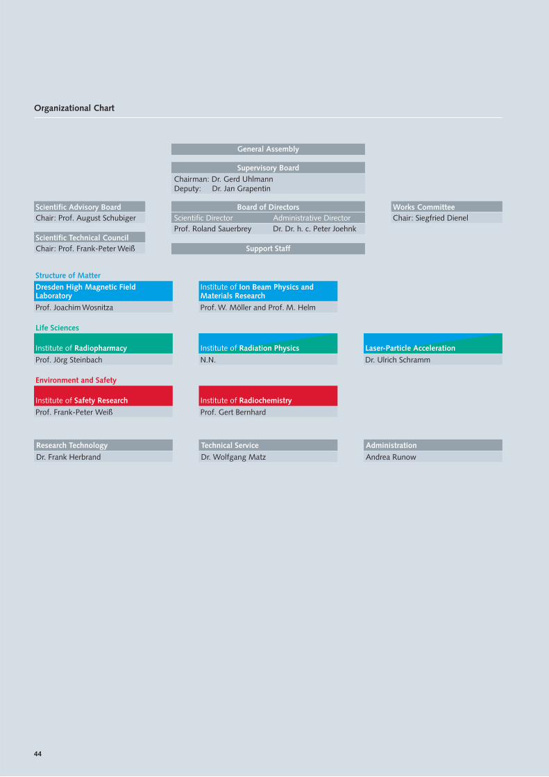
44
Structure of Matter
Life Sciences
Research Technology
Dr. Frank Herbrand
Administration
Andrea Runow
Technical Service
Dr. Wolfgang Matz
Institute of Ion Beam Physics andMaterials Research
Prof. W. Möller and Prof. M. Helm
Institute of Radiopharmacy
Prof. Jörg Steinbach
Dresden High Magnetic FieldLaboratory
Prof. Joachim Wosnitza
Institute of Radiation Physics
N.N.
Laser-Particle Acceleration
Dr. Ulrich Schramm
Environment and Safety
Institute of Safety Research
Prof. Frank-Peter Weiß
Institute of Radiochemistry
Prof. Gert Bernhard
General Assembly
Scientific Advisory Board Chair: Prof. August Schubiger
Supervisory BoardChairman: Dr. Gerd UhlmannDeputy: Dr. Jan Grapentin
Scientific Technical Council Chair: Prof. Frank-Peter Weiß
Works Committee Chair: Siegfried Dienel
Support Staff
Board of Directors Scientific Director Administrative DirectorProf. Roland Sauerbrey Dr. Dr. h. c. Peter Joehnk
Organizational Chart

IMPRINT
FZD Triennial Scientific Report 2004-2007 I Volume 1Volume 1 Structure of MatterVolume 2 Environment and SafetyVolume 3 Life Sciences
Published by Forschungszentrum Dresden-RossendorfConcept and editorial work Dr. Christine Bohnet & Anja Bartho, FZDDesign and layout WA Preußel, CoswigPhotos C. Preußel & FZD employeesAvailable from Forschungszentrum Dresden-Rossendorf
Public RelationsBautzner Landstr. 12801328 Dresden / GermanyPhone: +49 351 260 2450Email: [email protected]://www.fzd.de
ISSN 1437-322XWissenschaftlich-Technische BerichteFZD-470, October 2007
Copying is welcomed, provided the source is quoted.
Forschungszentrum Dresden-RossendorfP.O. Box 51 01 19 I 01314 Dresden/GermanyScientific Director I Prof. Dr. Roland SauerbreyPhone +49 351 260 2625Fax +49 351 260 2700Email [email protected]
Member of the Leibniz Association