Lecture 19. Sensors of Structure Matter Waves and the deBroglie wavelength Heisenberg uncertainty...
144
Lecture 19
-
date post
21-Dec-2015 -
Category
Documents
-
view
215 -
download
0
Transcript of Lecture 19. Sensors of Structure Matter Waves and the deBroglie wavelength Heisenberg uncertainty...
Lecture 19
Sensors of Structure
• Matter Waves and the deBroglie wavelength
• Heisenberg uncertainty principle
• Electron diffraction
• Transmission electron microscopy
• Atomic-resolution sensors
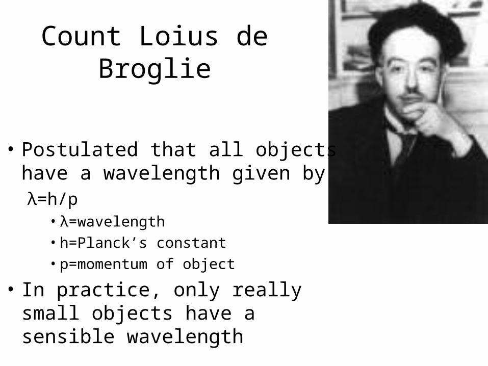
Count Loius de Broglie
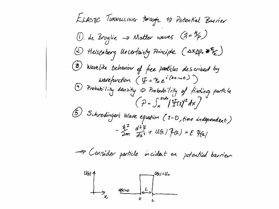
• Postulated that all objects have a wavelength given by λ=h/p
• λ=wavelength
• h=Planck’s constant
• p=momentum of object
• In practice, only really small objects have a sensible wavelength
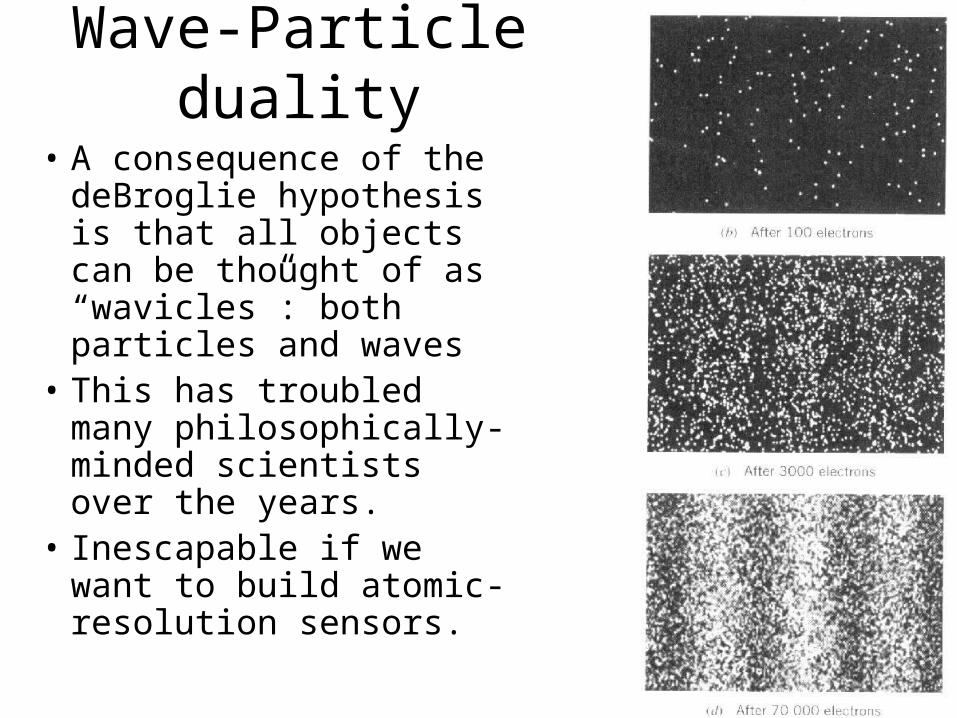
Wave-Particle duality
• A consequence of the deBroglie hypothesis is that all objects can be thought of as “wavicles”: both particles and waves
• This has troubled many philosophically-minded scientists over the years.
• Inescapable if we want to build atomic-resolution sensors.
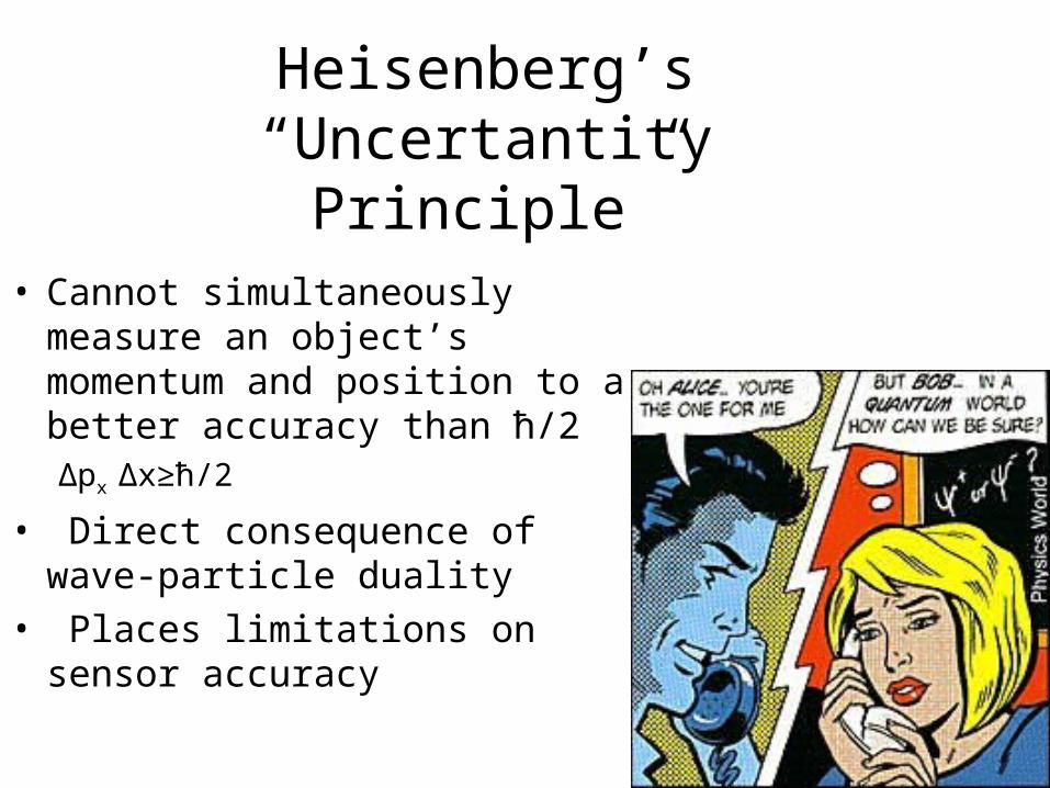
Heisenberg’s “Uncertantity Principle”
• Cannot simultaneously measure an object’s momentum and position to a better accuracy than ħ/2Δpx Δx≥ħ/2
• Direct consequence of wave-particle duality
• Places limitations on sensor accuracy
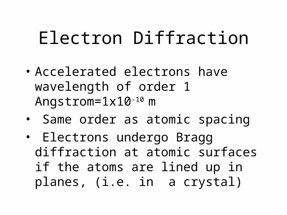
Electron Diffraction
• Accelerated electrons have wavelength of order 1 Angstrom=1x10⁻¹⁰ m
• Same order as atomic spacing
• Electrons undergo Bragg diffraction at atomic surfaces if the atoms are lined up in planes, (i.e. in a crystal)
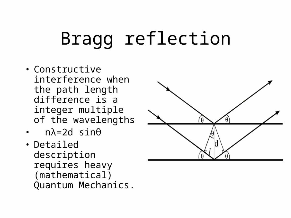
Bragg reflection
• Constructive interference when the path length difference is a integer multiple of the wavelengths
• nλ=2d sinθ• Detailed description
requires heavy (mathematical) Quantum Mechanics.
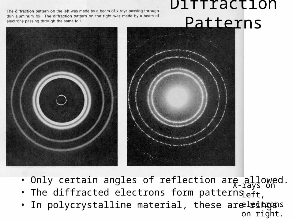
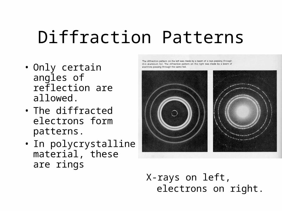
X-rays on left, electrons on right.
Diffraction Patterns
• Only certain angles of reflection are allowed.• The diffracted electrons form patterns.• In polycrystalline material, these are rings
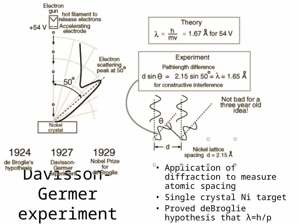
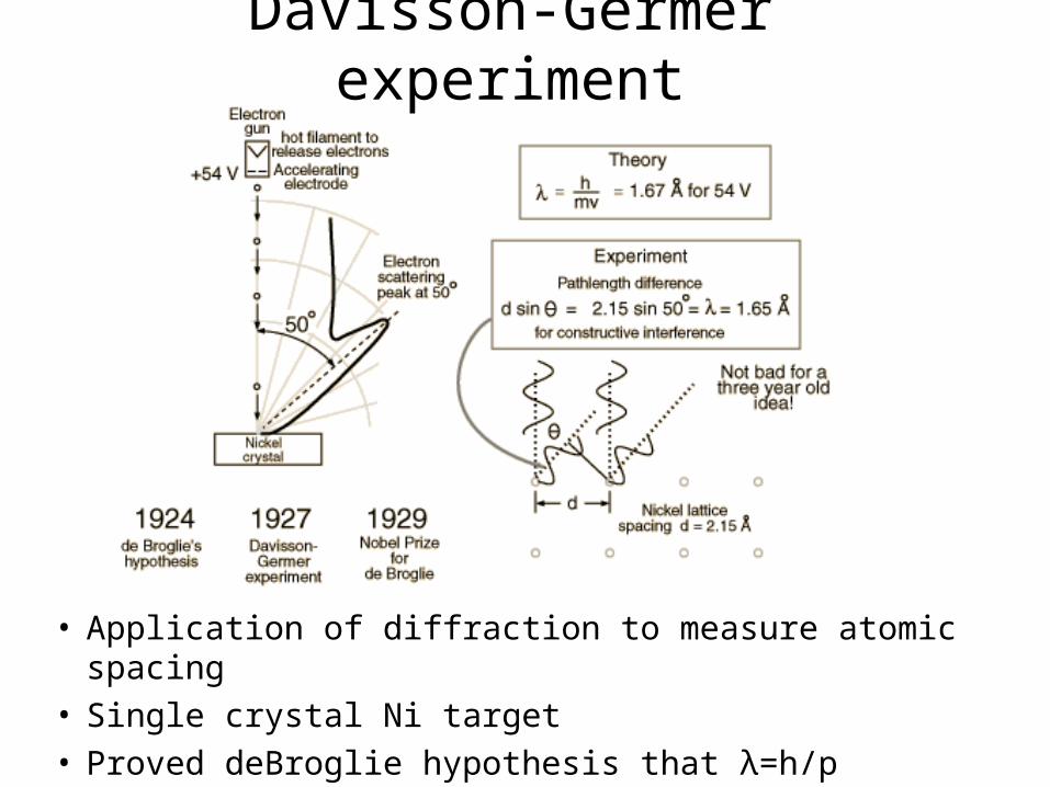
Davisson-Germer experiment
• Application of diffraction to measure atomic spacing
• Single crystal Ni target• Proved deBroglie hypothesis
that λ=h/p

Proof that λ=h/pAccelerated electrons have energy eV:
eV= ½ mv2 => v = (2Ve/m)1/2
de Broglie said:λ=h/p=h/(mv)=h/(2mVe)1/2=1.67 Å
Davisson-Germer found lattice spacing: λ=dsinθ=1.65 Å
Excellent agreement between theory and experiment!
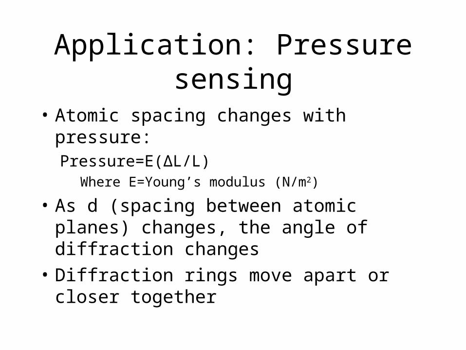
Application: Pressure sensing
• Atomic spacing changes with pressure:Pressure=E(ΔL/L)
Where E=Young’s modulus (N/m2)
• As d (spacing between atomic planes) changes, the angle of diffraction changes
• Diffraction rings move apart or closer together

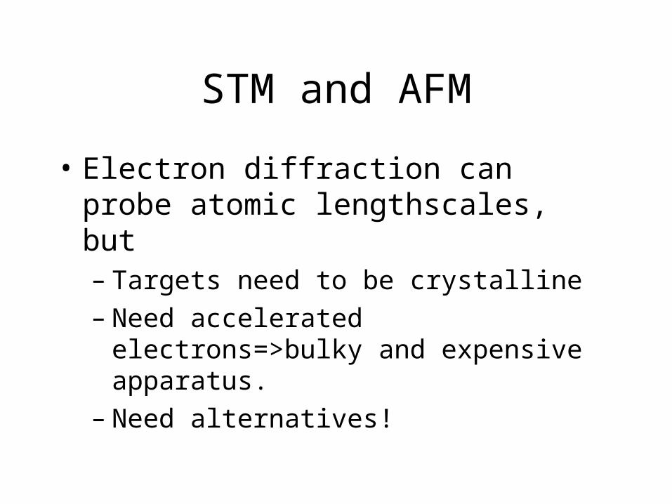
STM and AFM
• Electron diffraction can probe atomic lengthscales, but– Targets need to be crystalline– Need accelerated electrons=>bulky and
expensive apparatus.– Need alternatives!
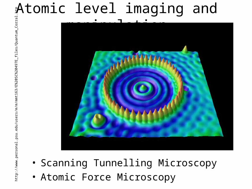
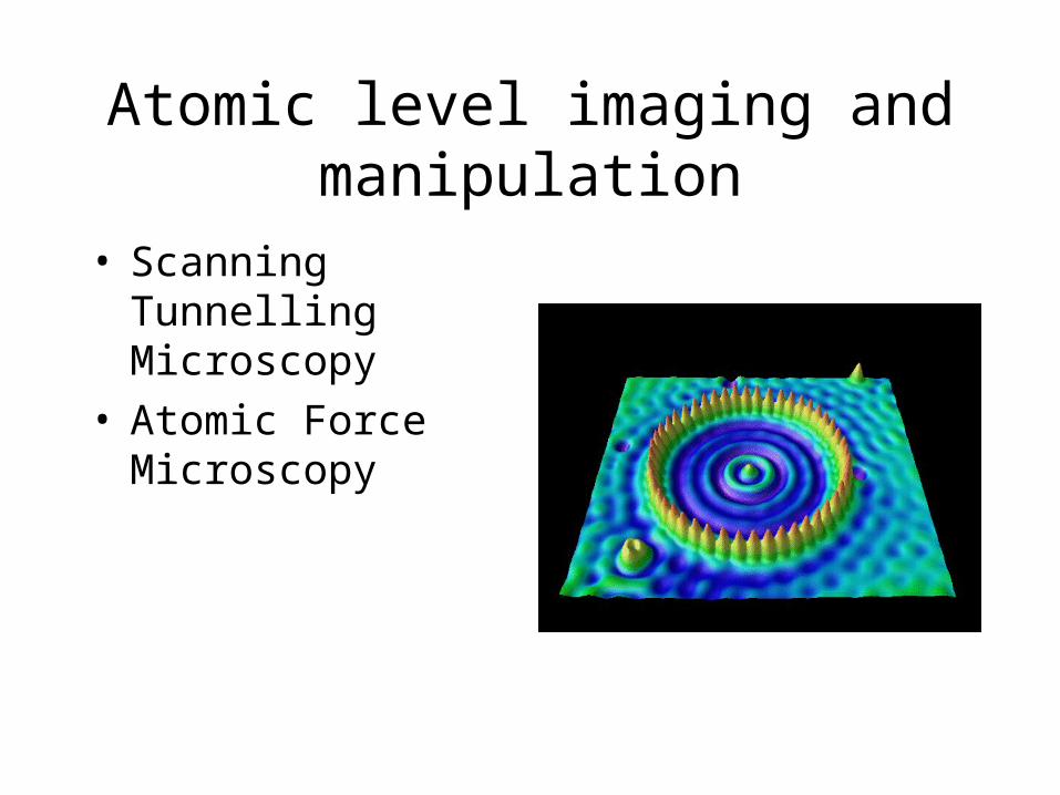
Atomic level imaging and manipulation
• Scanning Tunnelling Microscopy • Atomic Force Microscopy
http
://w
ww
.per
sona
l.psu
.edu
/use
rs/m
/m/m
mt1
63/E
%20
SC%
2049
7E_f
iles/
Qua
ntum
_Cor
ral.h
tm
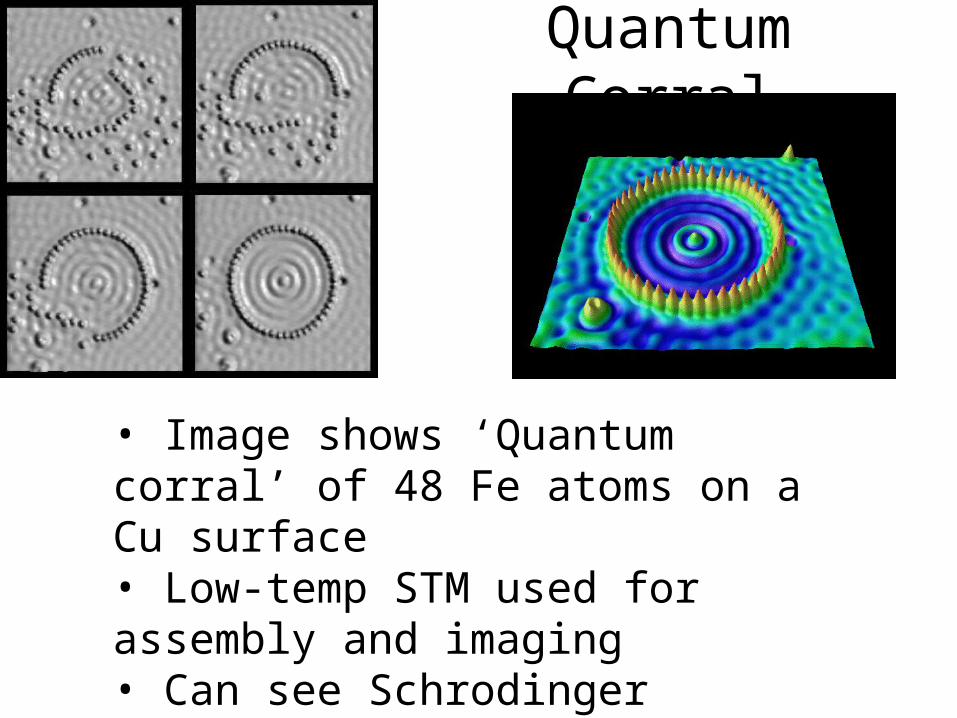
• Image shows ‘Quantum corral’ of 48 Fe atoms on a Cu surface• Low-temp STM used for assembly and imaging• Can see Schrodinger standing waves• Colors artificial
Quantum Corral
Quantum Mechanics
• STM and AFM inherently quantum-mechanical in operation
• Need to understand the electron wavefunction to understand their operation
• We need some QM first

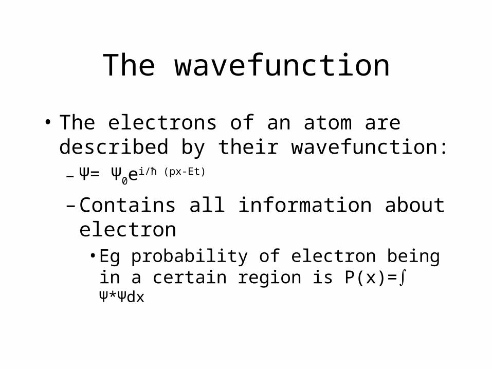
The wavefunction
• The electrons of an atom are described by their wavefunction:– Ψ= Ψ0ei/ħ (px-Et)
– Contains all information about electron• Eg probability of electron being in a certain
region is P(x)=∫ Ψ*Ψdx

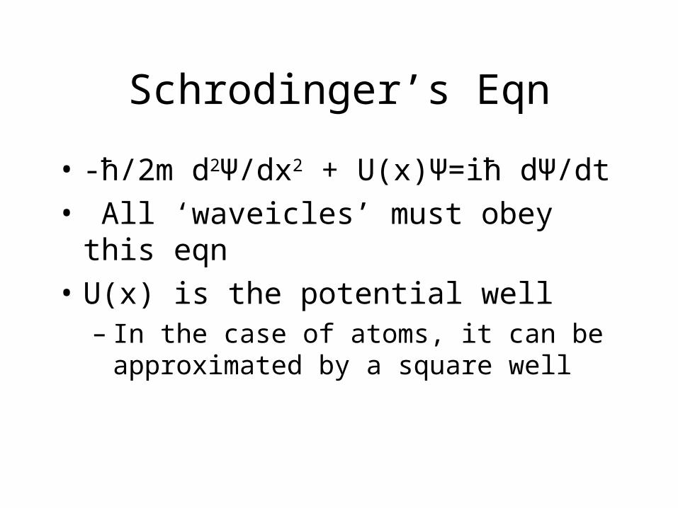
Schrodinger’s Eqn
• -ħ/2m d2Ψ/dx2 + U(x)Ψ=iħ dΨ/dt
• All ‘waveicles’ must obey this eqn
• U(x) is the potential well– In the case of atoms, it can be approximated by
a square well
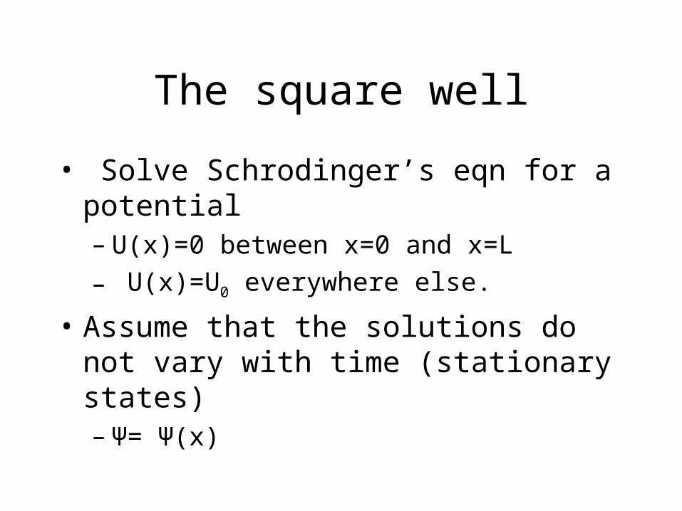
The square well
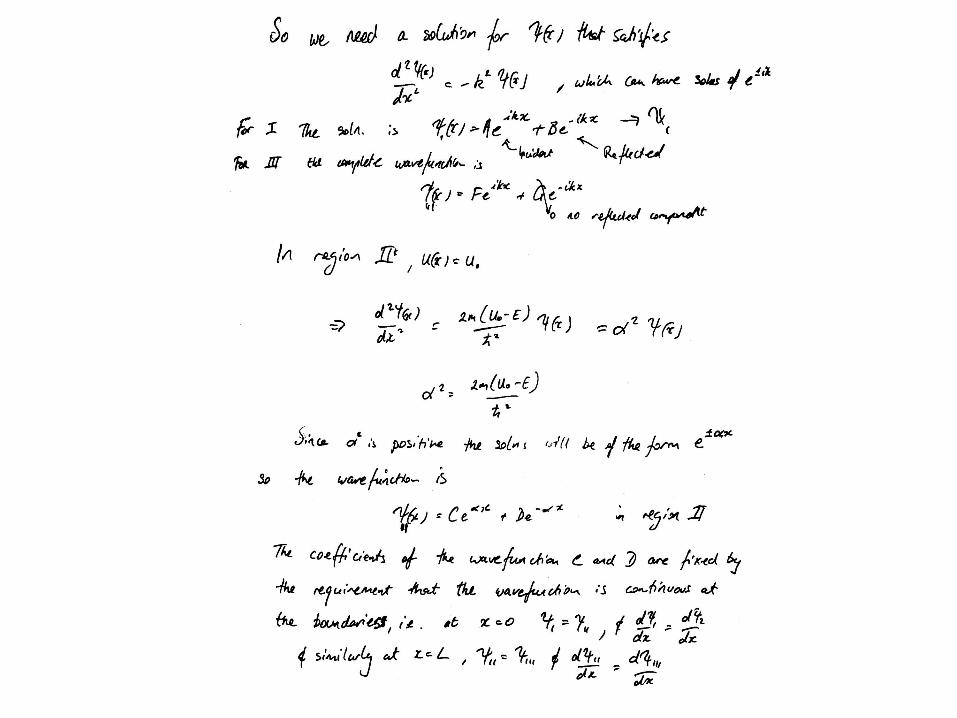
• Solve Schrodinger’s eqn for a potential– U(x)=0 between x=0 and x=L
– U(x)=U0 everywhere else.
• Assume that the solutions do not vary with time (stationary states)– Ψ= Ψ(x)
Solutions for a square well
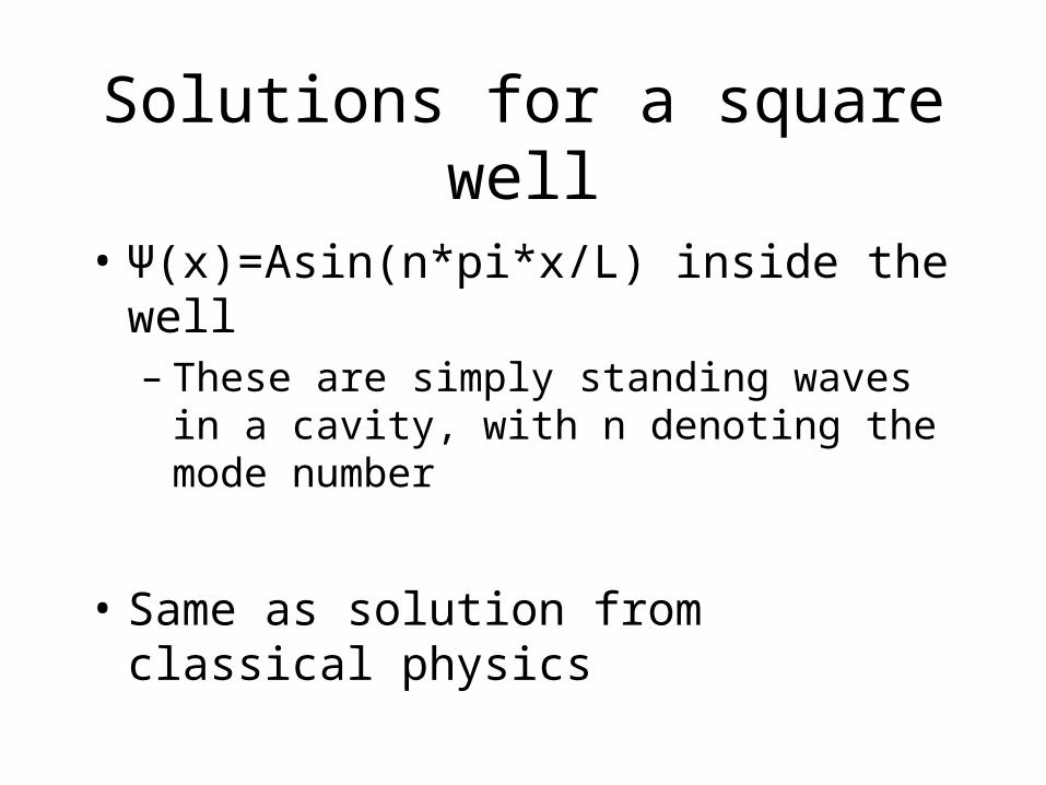
• Ψ(x)=Asin(n*pi*x/L) inside the well– These are simply standing waves in a cavity,
with n denoting the mode number
• Same as solution from classical physics
Wavefunction trails
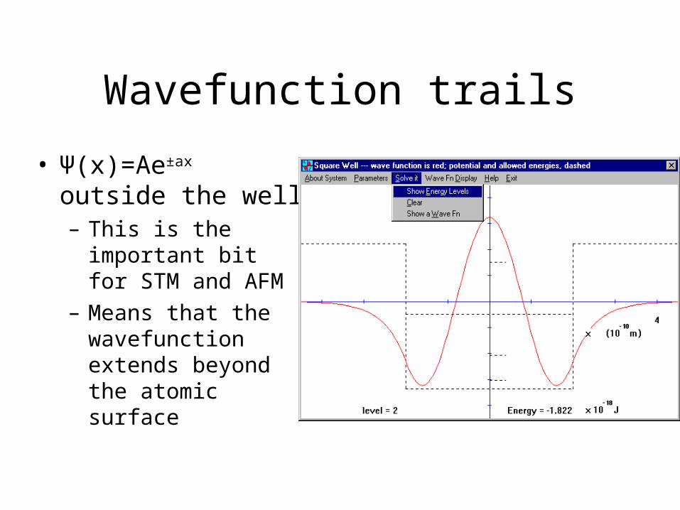
• Ψ(x)=Ae±ax outside the well– This is the important
bit for STM and AFM
– Means that the wavefunction extends beyond the atomic surface
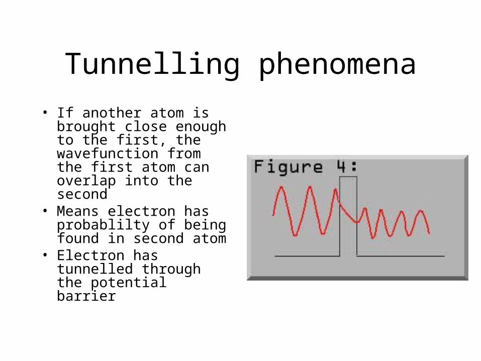
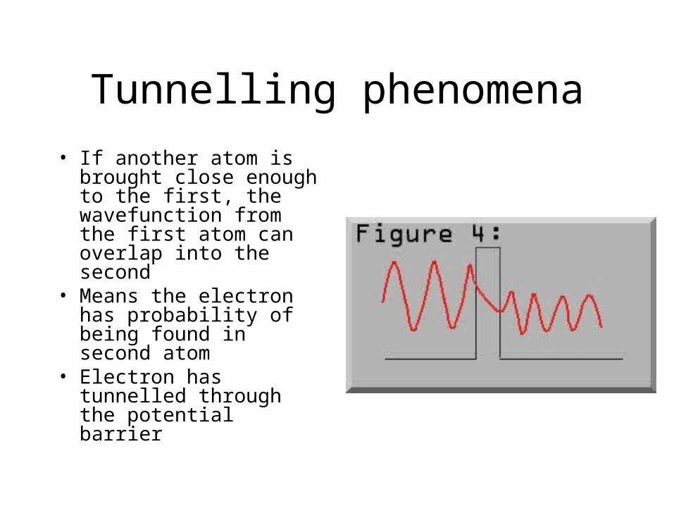
Tunnelling phenomena
• If another atom is brought close enough to the first, the wavefunction from the first atom can overlap into the second
• Means electron has probablilty of being found in second atom
• Electron has tunnelled through the potential barrier
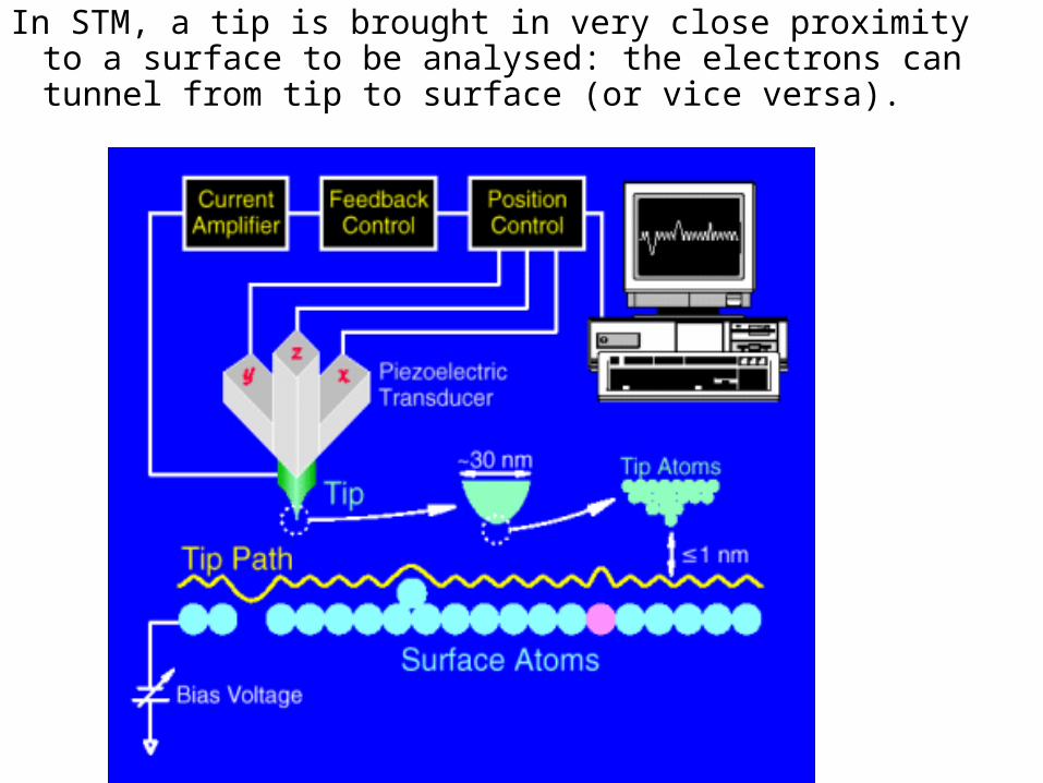
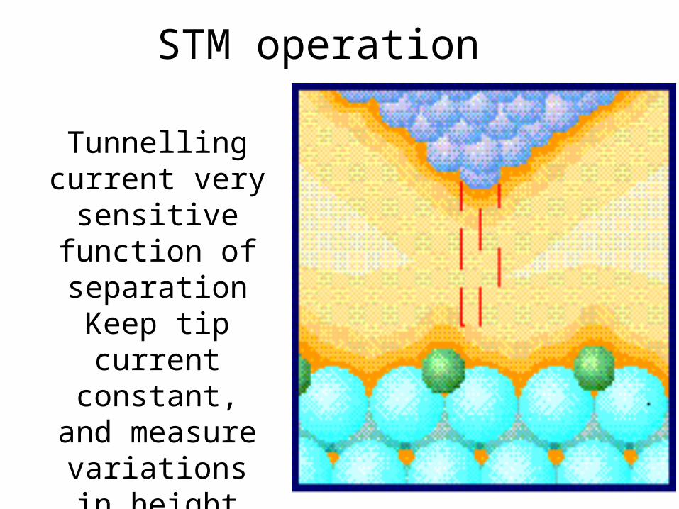
In STM, a tip is brought in very close proximity to a surface to be analysed: the electrons can tunnel from tip to surface (or vice versa).
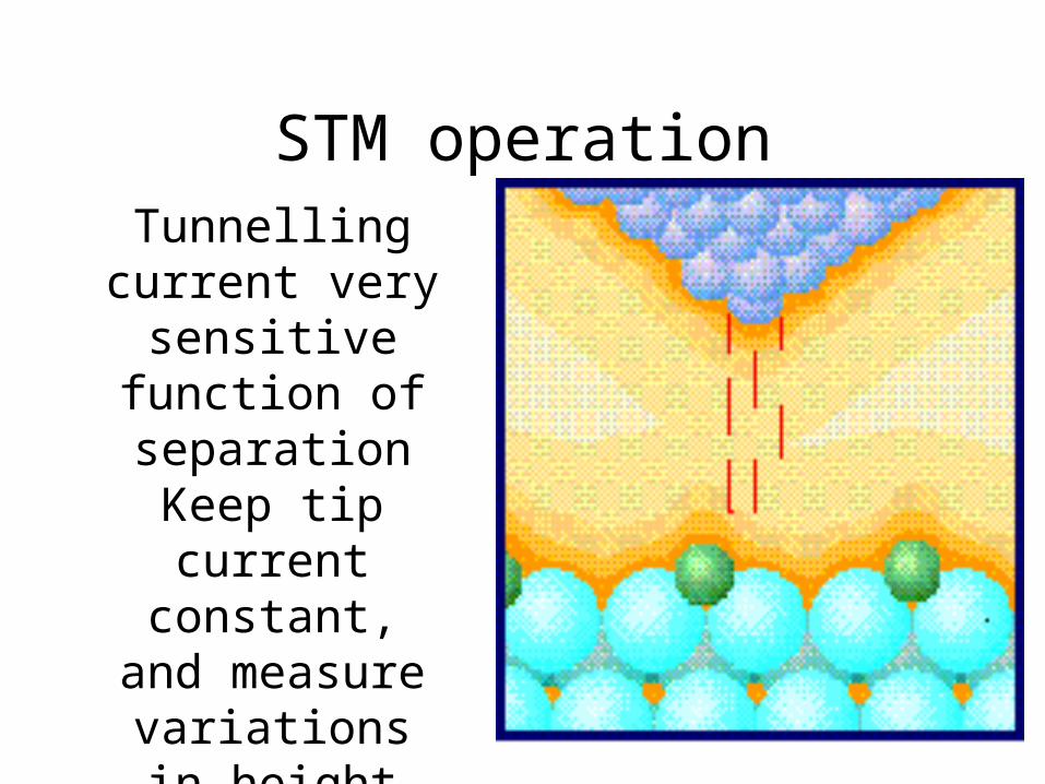
STM operationTunnelling current
very sensitive function of separation
Keep tip current constant, and
measure variations in height with a
piezoelectric crystal
Lecture 20

Sensors of Structure
• Matter Waves and the deBroglie wavelength
• Heisenberg uncertainty principle
• Electron diffraction
• Transmission electron microscopy
• Atomic-resolution sensors
deBroglie
• Postulated that all objects have a wavelength given by – λ=h/p
• λ=wavelength
• h=Planck’s constant
• p=momentum of object
• In practice, only really small objects have a sensible wavelength
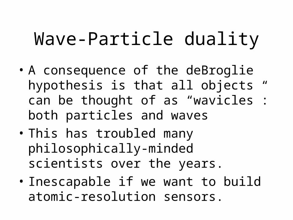
Wave-Particle duality
• A consequence of the deBroglie hypothesis is that all objects can be thought of as “wavicles”: both particles and waves
• This has troubled many philosophically-minded scientists over the years.
• Inescapable if we want to build atomic-resolution sensors.
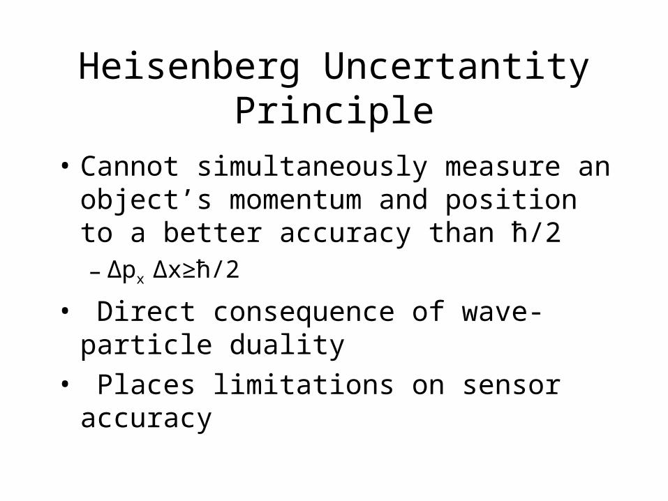
Heisenberg Uncertantity Principle
• Cannot simultaneously measure an object’s momentum and position to a better accuracy than ħ/2– Δpx Δx≥ħ/2
• Direct consequence of wave-particle duality
• Places limitations on sensor accuracy
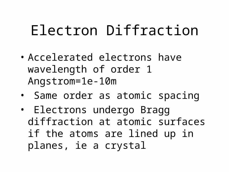
Electron Diffraction
• Accelerated electrons have wavelength of order 1 Angstrom=1e-10m
• Same order as atomic spacing
• Electrons undergo Bragg diffraction at atomic surfaces if the atoms are lined up in planes, ie a crystal
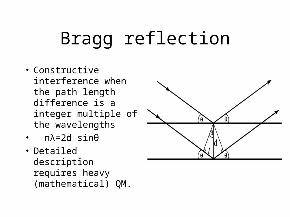
Bragg reflection
• Constructive interference when the path length difference is a integer multiple of the wavelengths
• nλ=2d sinθ• Detailed description
requires heavy (mathematical) QM.
Diffraction Patterns
• Only certain angles of reflection are allowed.
• The diffracted electrons form patterns.
• In polycrystalline material, these are rings
X-rays on left, electrons on right.
Davisson-Germer experiment
• Application of diffraction to measure atomic spacing• Single crystal Ni target• Proved deBroglie hypothesis that λ=h/p
Proof that λ=h/pAccelerated electrons have energy eV:
eV= ½ mv2 => v = (2Ve/m)1/2
de Broglie said:λ=h/p=h/(mv)=h/(2mVe)1/2=1.67 Å
Davisson-Germer found lattice spacing: λ=dsinθ=1.65 Å
Excellent agreement between theory and experiment!
Pressure sensing
• Atomic spacing changes with pressure:– Pressure=E(ΔL/L)
• E=Youngs modulus (N/m2)
• As d changes, angle of diffraction changes
• Rings move apart or closer together
STM and AFM
• Electron diffraction can probe atomic lengthscales, but– Targets need to be crystalline– Need accelerated electrons=>bulky and
expensive apparatus.– Need alternatives!

Atomic level imaging and manipulation
• Scanning Tunnelling Microscopy • Atomic Force Microscopy
http
://w
ww
.per
sona
l.psu
.edu
/use
rs/m
/m/m
mt1
63/E
%20
SC%
2049
7E_f
iles/
Qua
ntum
_Cor
ral.h
tm

• Image shows ‘Quantum corral’ of 48 Fe atoms on a Cu surface• Low-temp STM used for assembly and imaging• Can see Schrodinger standing waves• Colors artificial
Quantum Corral

Quantum Mechanics
• STM and AFM inherently quantum-mechanical in operation
• Need to understand the electron wavefunction to understand their operation
• We need some QM first
The wavefunction
• The electrons of an atom are described by their wavefunction:– Ψ= Ψ0ei/ħ (px-Et)
– Contains all information about electron• Eg probability of electron being in a certain
region is P(x)=∫ Ψ*Ψdx
Schrodinger’s Eqn
• -ħ/2m d2Ψ/dx2 + U(x)Ψ=iħ dΨ/dt
• All ‘waveicles’ must obey this eqn
• U(x) is the potential well– In the case of atoms, it can be approximated by
a square well

The square well
• Solve Schrodinger’s eqn for a potential– U(x)=0 between x=0 and x=L
– U(x)=U0 everywhere else.
• Assume that the solutions do not vary with time (stationary states)– Ψ= Ψ(x)

Solutions for a square well
• Ψ(x)=Asin(n*pi*x/L) inside the well– These are simply standing waves in a cavity,
with n denoting the mode number
• Same as solution from classical physics

Wavefunction trails
• Ψ(x)=Ae±ax outside the well– This is the important
bit for STM and AFM
– Means that the wavefunction extends beyond the atomic surface
Atomic level imaging and manipulation
• Scanning Tunnelling Microscopy
• Atomic Force Microscopy
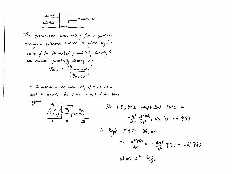
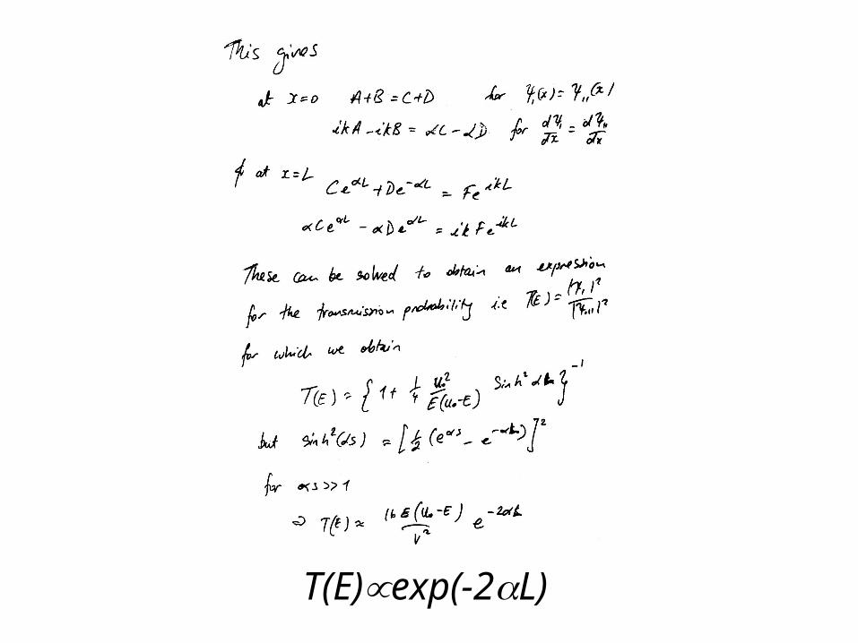
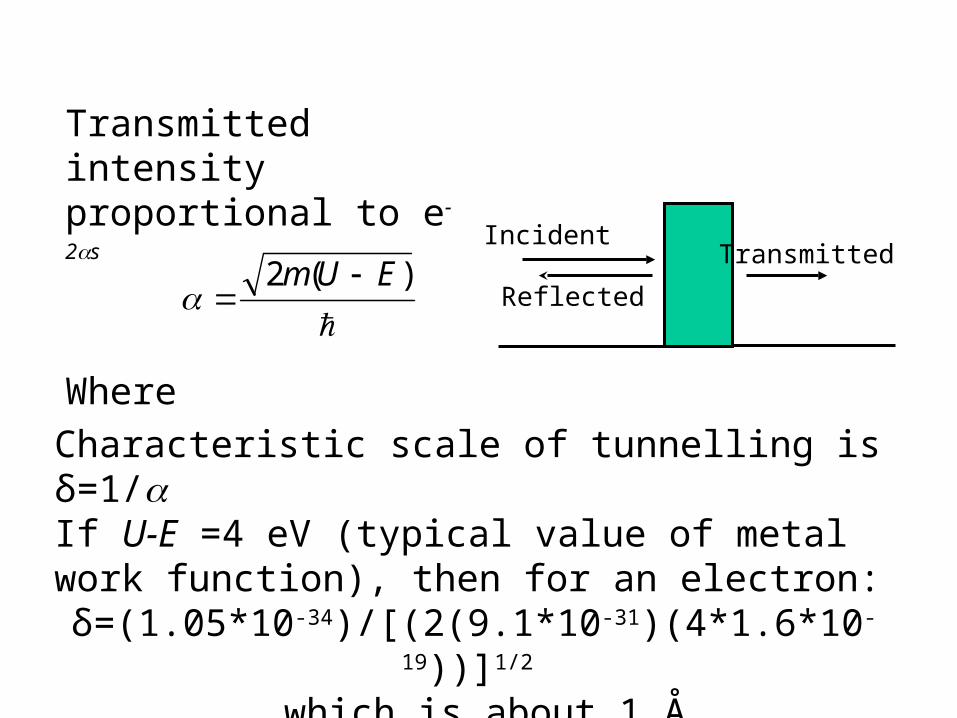
T(E)exp(-2L)
Tunnelling phenomena
• If another atom is brought close enough to the first, the wavefunction from the first atom can overlap into the second
• Means the electron has probability of being found in second atom
• Electron has tunnelled through the potential barrier
Incident
Reflected
Transmitted
Transmitted intensityproportional to e-2s
Where )(2 EUm
Characteristic scale of tunnelling is δ=1/If U-E =4 eV (typical value of metal work function), then for an electron:
δ=(1.05*10-34)/[(2(9.1*10-31)(4*1.6*10-19))]1/2
which is about 1 Å

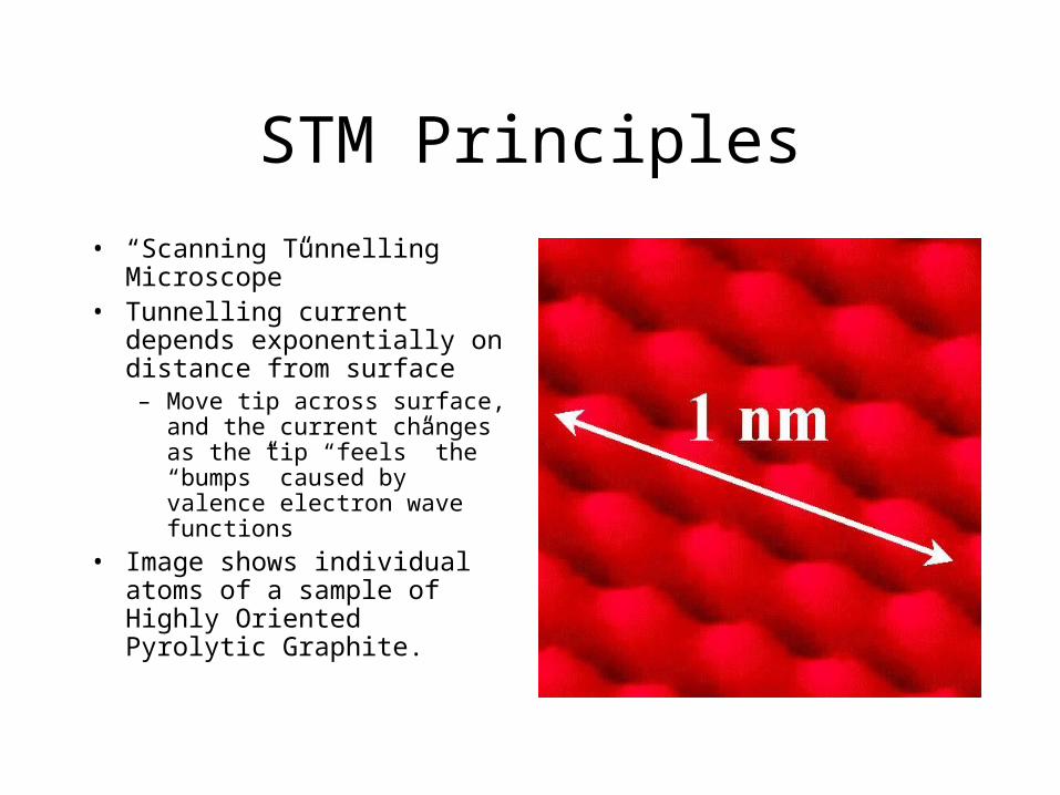
STM Principles
• “Scanning Tunnelling Microscope”
• Tunnelling current depends exponentially on distance from surface– Move tip across surface, and
the current changes as the tip “feels” the “bumps” caused by valence electron wave functions
• Image shows individual atoms of a sample of Highly Oriented Pyrolytic Graphite.

In STM, a tip is brought in very close proximity to a surface to be analysed: the electrons can tunnel from tip to surface (or vice versa).
STM operation
Tunnelling current very sensitive
function of separation
Keep tip current constant, and
measure variations in height with a
piezoelectric crystal
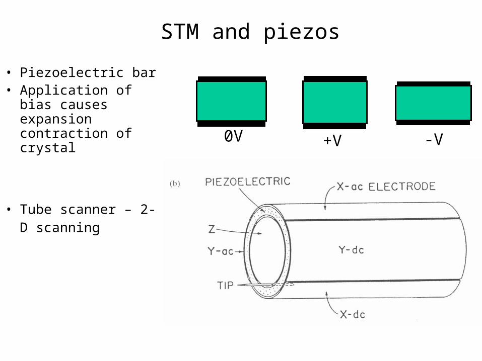
• Piezoelectric bar• Application of bias
causes expansion contraction of crystal
• Tube scanner – 2-D scanning
0V -V+V
STM and piezos
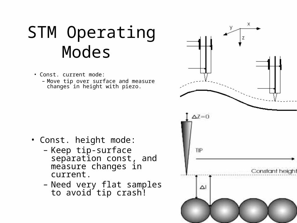
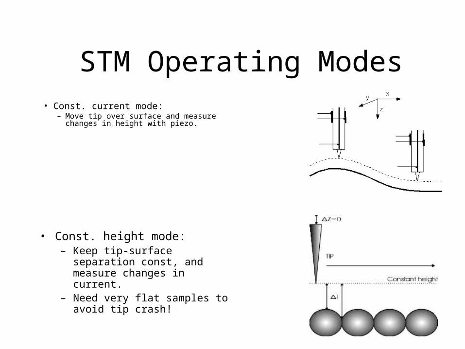
STM Operating Modes
• Const. height mode:– Keep tip-surface separation
const, and measure changes in current.
– Need very flat samples to avoid tip crash!
• Const. current mode:– Move tip over surface and measure changes
in height with piezo.
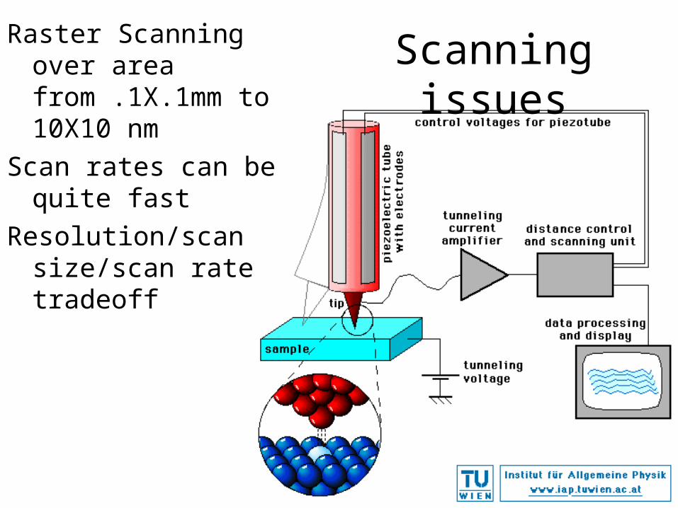
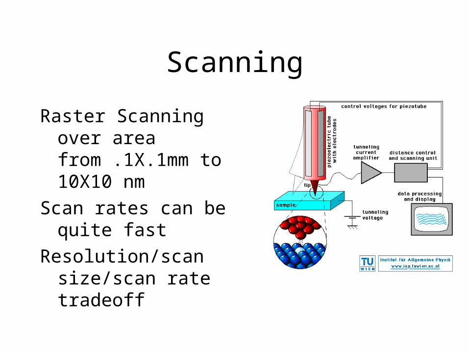
Scanning issuesRaster Scanning over
area from .1X.1mm to 10X10 nm
Scan rates can be quite fast
Resolution/scan size/scan rate tradeoff
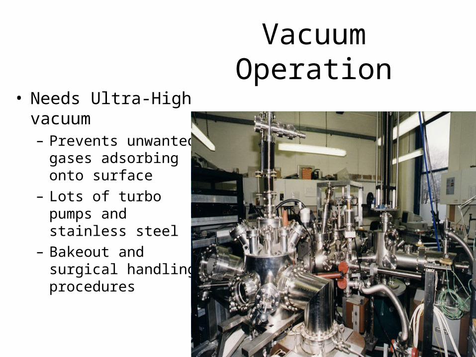
Vacuum Operation
• Needs Ultra-High vacuum– Prevents unwanted
gases adsorbing onto surface
– Lots of turbo pumps and stainless steel
– Bakeout and surgical handling procedures
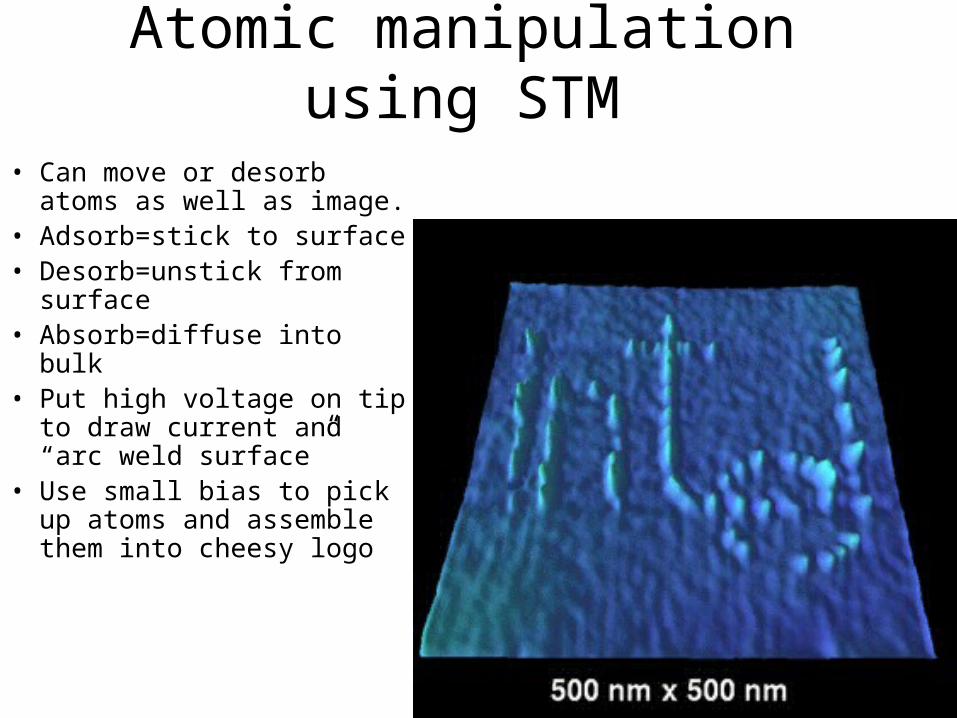
Atomic manipulation using STM
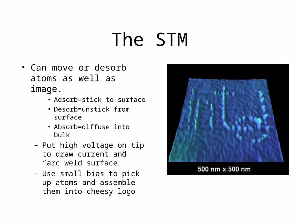
• Can move or desorb atoms as well as image.
• Adsorb=stick to surface• Desorb=unstick from
surface• Absorb=diffuse into bulk• Put high voltage on tip to
draw current and “arc weld surface”
• Use small bias to pick up atoms and assemble them into cheesy logo

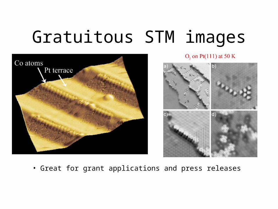
Some gratuitous STM images
• Great for grant applications and press releases!
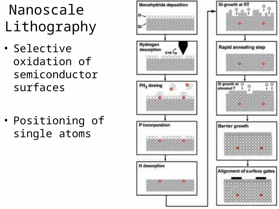
Nanoscale Lithography
• Selective oxidation of semiconductor surfaces
• Positioning of single atoms
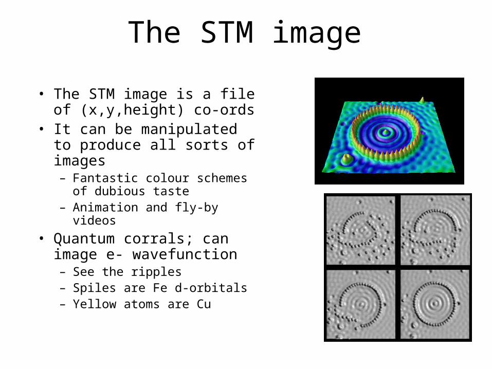
The STM image
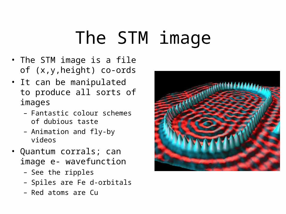
• The STM image is a file of (x,y,height) co-ords
• It can be manipulated to produce all sorts of images– Fantastic colour schemes of
dubious taste– Animation and fly-by videos
• Quantum corrals; can image e- wavefunction– See the ripples– Spiles are Fe d-orbitals– Yellow atoms are Cu
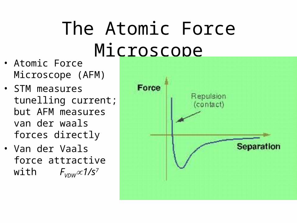
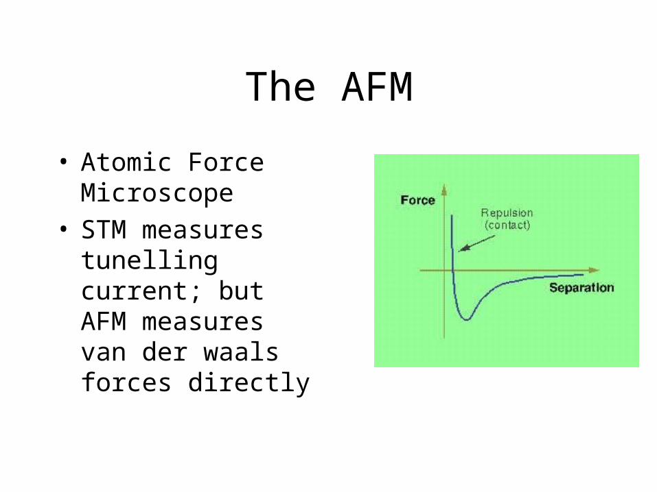
The Atomic Force Microscope• Atomic Force Microscope
(AFM)
• STM measures tunelling current; but AFM measures van der waals forces directly
• Van der Vaals force attractive with FVDW1/s7
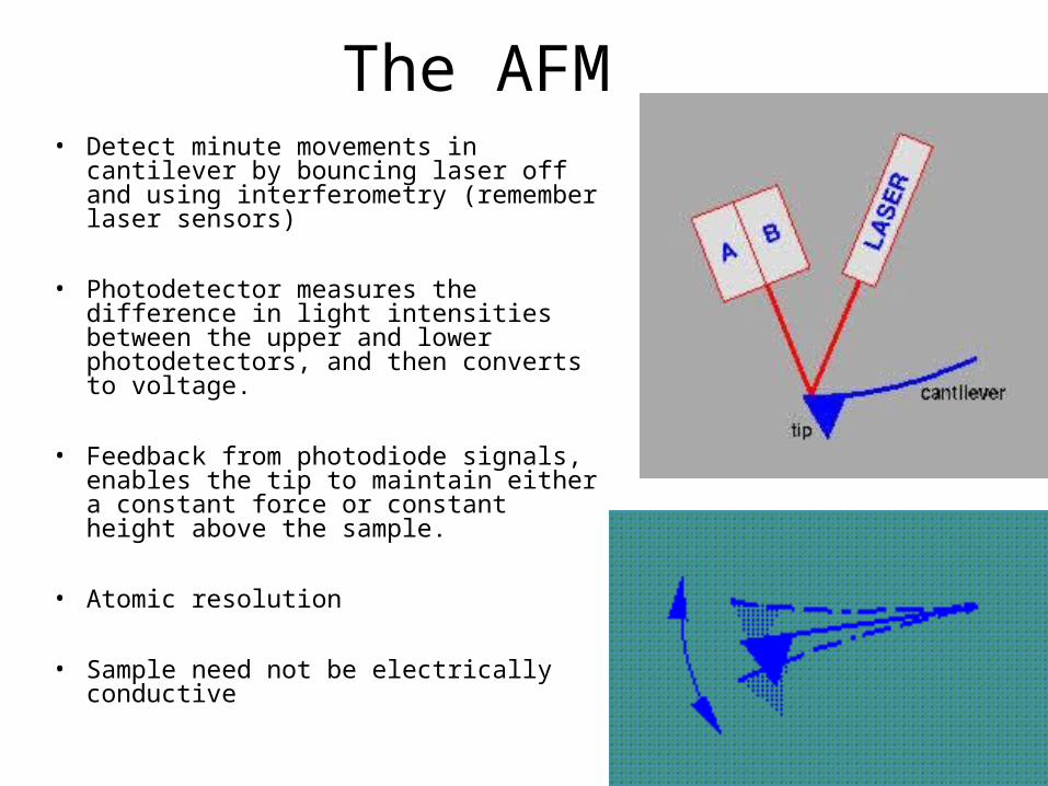
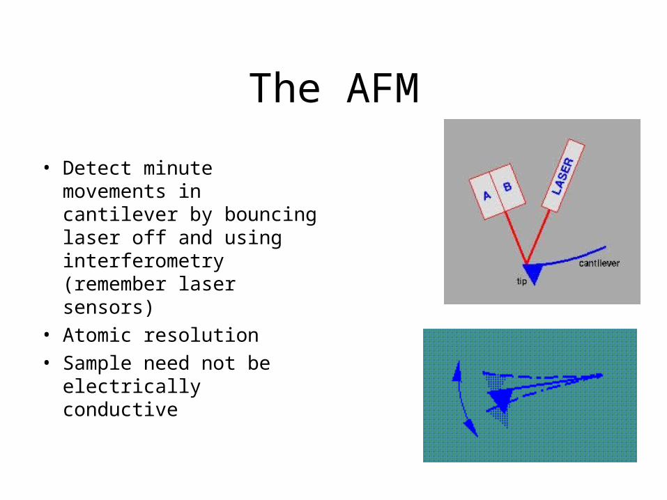
The AFM• Detect minute movements in cantilever by
bouncing laser off and using interferometry (remember laser sensors)
• Photodetector measures the difference in light intensities between the upper and lower photodetectors, and then converts to voltage.
• Feedback from photodiode signals, enables the tip to maintain either a constant force or constant height above the sample.
• Atomic resolution
• Sample need not be electrically conductive
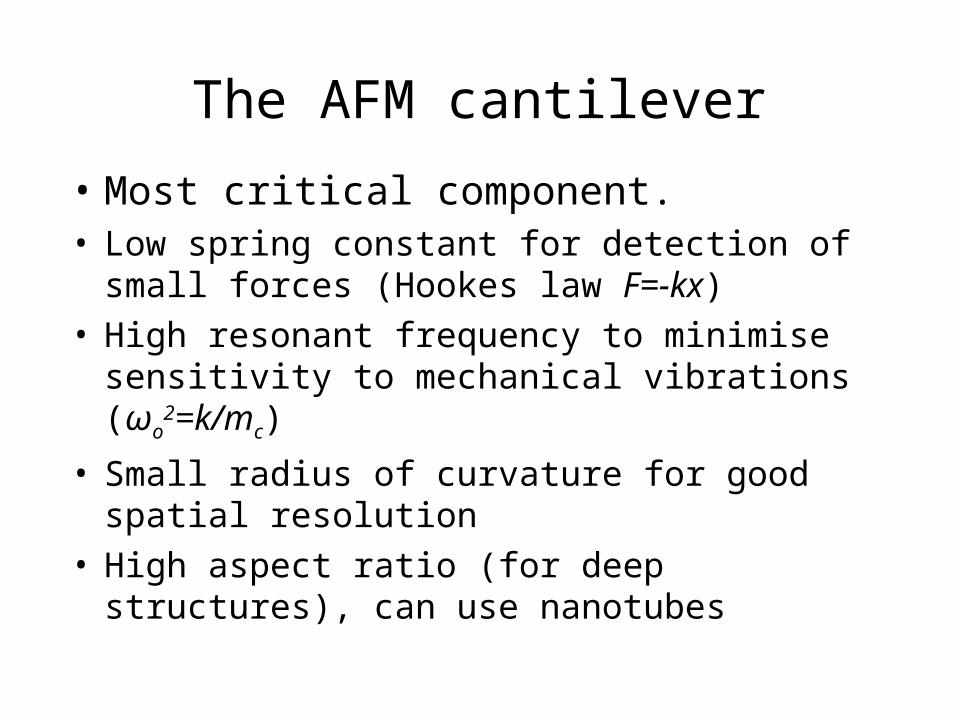
The AFM cantilever
• Most critical component.• Low spring constant for detection of small forces
(Hookes law F=-kx) • High resonant frequency to minimise sensitivity to
mechanical vibrations (ωo2=k/mc)
• Small radius of curvature for good spatial resolution
• High aspect ratio (for deep structures), can use nanotubes
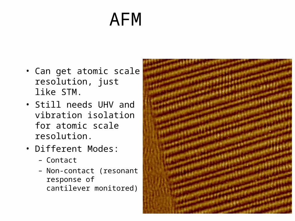
AFM
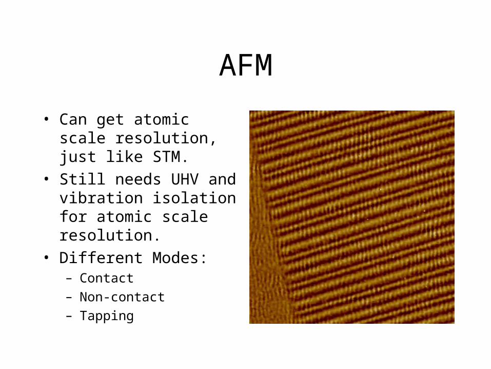
• Can get atomic scale resolution, just like STM.
• Still needs UHV and vibration isolation for atomic scale resolution.
• Different Modes:– Contact
– Non-contact (resonant response of cantilever monitored)
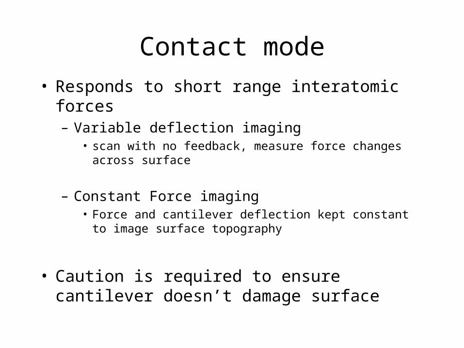
Contact mode
• Responds to short range interatomic forces– Variable deflection imaging
• scan with no feedback, measure force changes across surface
– Constant Force imaging• Force and cantilever deflection kept constant to image surface
topography
• Caution is required to ensure cantilever doesn’t damage surface
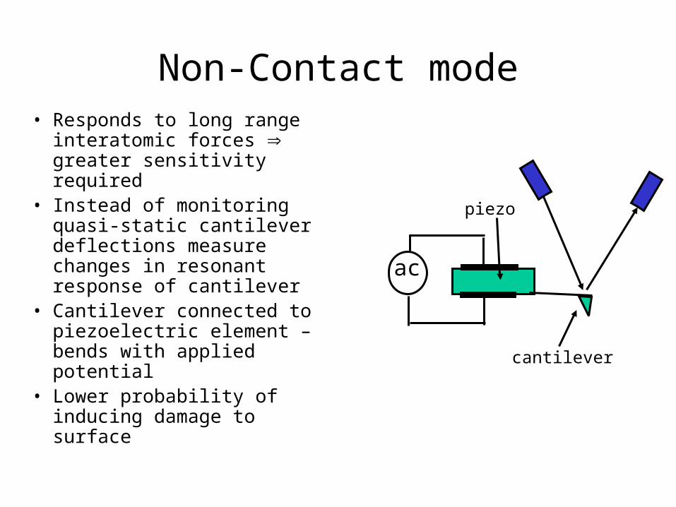
Non-Contact mode• Responds to long range
interatomic forces greater sensitivity required
• Instead of monitoring quasi-static cantilever deflections measure changes in resonant response of cantilever
• Cantilever connected to piezoelectric element – bends with applied potential
• Lower probability of inducing damage to surface
ac
cantilever
piezo
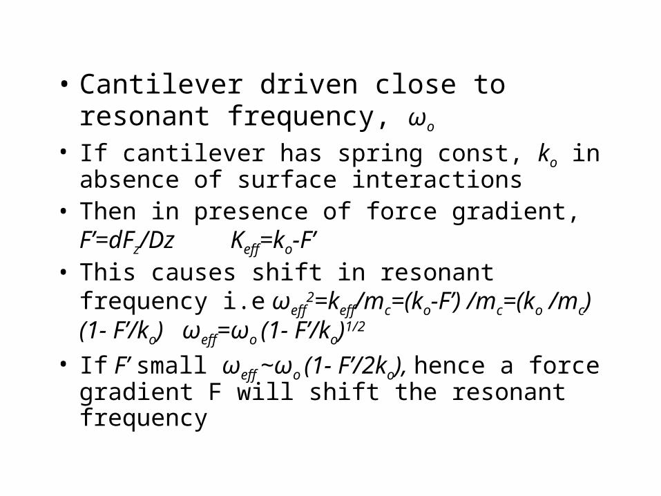
• Cantilever driven close to resonant frequency, ωo
• If cantilever has spring const, ko in absence of surface interactions
• Then in presence of force gradient, F’=dFz/Dz Keff=ko-F’
• This causes shift in resonant frequency i.e ωeff
2=keff/mc=(ko-F’) /mc=(ko /mc)(1- F’/ko) ωeff=ωo (1- F’/ko)1/2
• If F’ small ωeff ~ωo (1- F’/2ko), hence a force gradient F will shift the resonant frequency
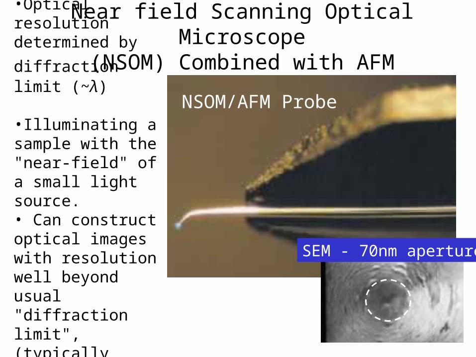
Near field Scanning Optical Microscope(NSOM) Combined with AFM
SEM - 70nm aperture
NSOM/AFM Probe•Optical resolution determined by
diffraction limit (~λ) •Illuminating a sample with the "near-field" of a small light source.• Can construct optical images with resolution well beyond usual "diffraction limit", (typically ~50 nm.)
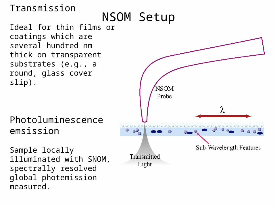
NSOM SetupTransmission
Ideal for thin films or coatings which are several hundred nm thick on transparent substrates (e.g., a round, glass cover slip).
Photoluminescence emsission
Sample locally illuminated with SNOM, spectrally resolved global photemission measured.
Lecture 21
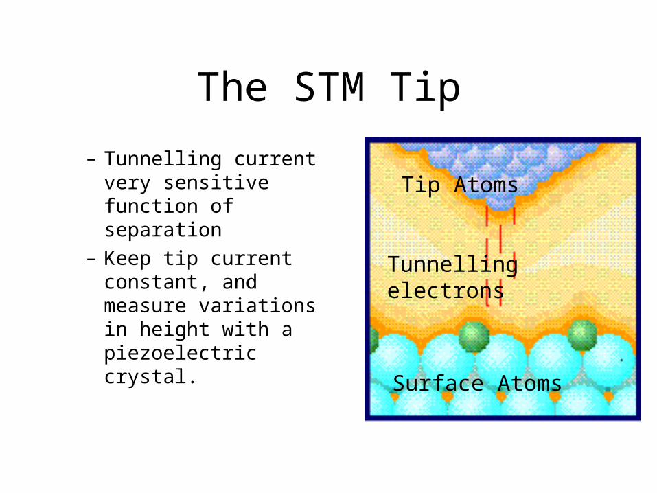
The STM Tip
– Tunnelling current very sensitive function of separation
– Keep tip current constant, and measure variations in height with a piezoelectric crystal.
Tip Atoms
Surface Atoms
Tunnelling electrons
STM Principles
• “Scanning Tunnelling Microscope”
• Tunnelling current depends exponentially on distance from surface– Move tip across surface, and
the current changes as the tip “feels” the “bumps” caused by valence electron wave functions
• Image shows individual atoms of a sample of Highly Oriented Pyrolytic Graphite.
STM Operating Modes
• Const. height mode:– Keep tip-surface separation const,
and measure changes in current.– Need very flat samples to avoid
tip crash!
• Const. current mode:– Move tip over surface and measure changes in
height with piezo.
Scanning
Raster Scanning over area from .1X.1mm to 10X10 nm
Scan rates can be quite fast
Resolution/scan size/scan rate tradeoff

Vacuum Sucks
• Needs Ultra-High vacuum– Otherwise unwanted
gases adsorb onto surface
– Lots of turbo pumps and stainless steel
– Bakeout and surgical handling procedures
The STM• Can move or desorb atoms
as well as image.• Adsorb=stick to surface
• Desorb=unstick from surface
• Absorb=diffuse into bulk
– Put high voltage on tip to draw current and “arc weld surface”
– Use small bias to pick up atoms and assemble them into cheesy logo
The STM image• The STM image is a file of
(x,y,height) co-ords
• It can be manipulated to produce all sorts of images– Fantastic colour schemes of
dubious taste
– Animation and fly-by videos
• Quantum corrals; can image e- wavefunction– See the ripples
– Spiles are Fe d-orbitals
– Red atoms are Cu
Gratuitous STM images
• Great for grant applications and press releases
The AFM
• Atomic Force Microscope
• STM measures tunelling current; but AFM measures van der waals forces directly
The AFM
• Detect minute movements in cantilever by bouncing laser off and using interferometry (remember laser sensors)
• Atomic resolution
• Sample need not be electrically conductive
AFM
• Can get atomic scale resolution, just like STM.
• Still needs UHV and vibration isolation for atomic scale resolution.
• Different Modes:– Contact
– Non-contact
– Tapping
Lecture 22

Lecture 23
Remember Dielectric Materials?
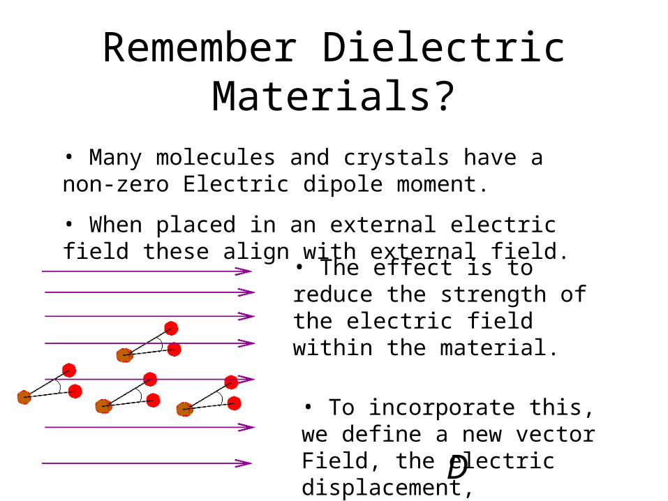
• Many molecules and crystals have a non-zero Electric dipole moment.
• When placed in an external electric field these align with external field.
• The effect is to reduce the strength of the electric field within the material.
• To incorporate this, we define a new vector Field, the electric displacement, D
Diamagnetism
• Polarisation of dielectrics involves the creation of induced electric dipoles by an external electric field
• The equivalent effect for magnetic materials is diamagnetism
• The atoms in a diamagnet alter their electron orbits in order to oppose the field
• Diamagnet acts like a bar magnet and repels external field
• Water is a diamagnet-hence the levitating frog!
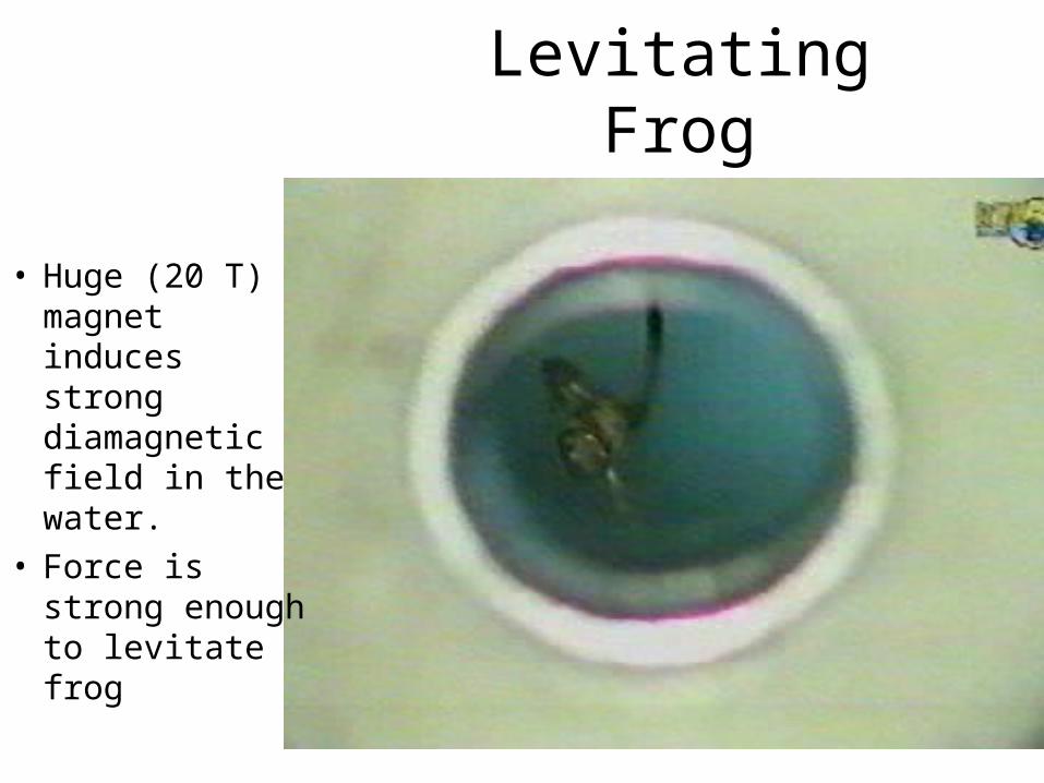
Levitating Frog
• Huge (20 T) magnet induces strong diamagnetic field in the water.
• Force is strong enough to levitate frog
Paramagnetism
• In some materials, there are permanent magnetic moments.
• When an external magnetic field is applied, these line up with the field to reinforce it
• This is a much stronger effect than diamagnetism, and in the opposite effect
• Ferromagnetism is a form of paramagnetism• Where do these permanent magnetic moments
originate from?
Magnetisation
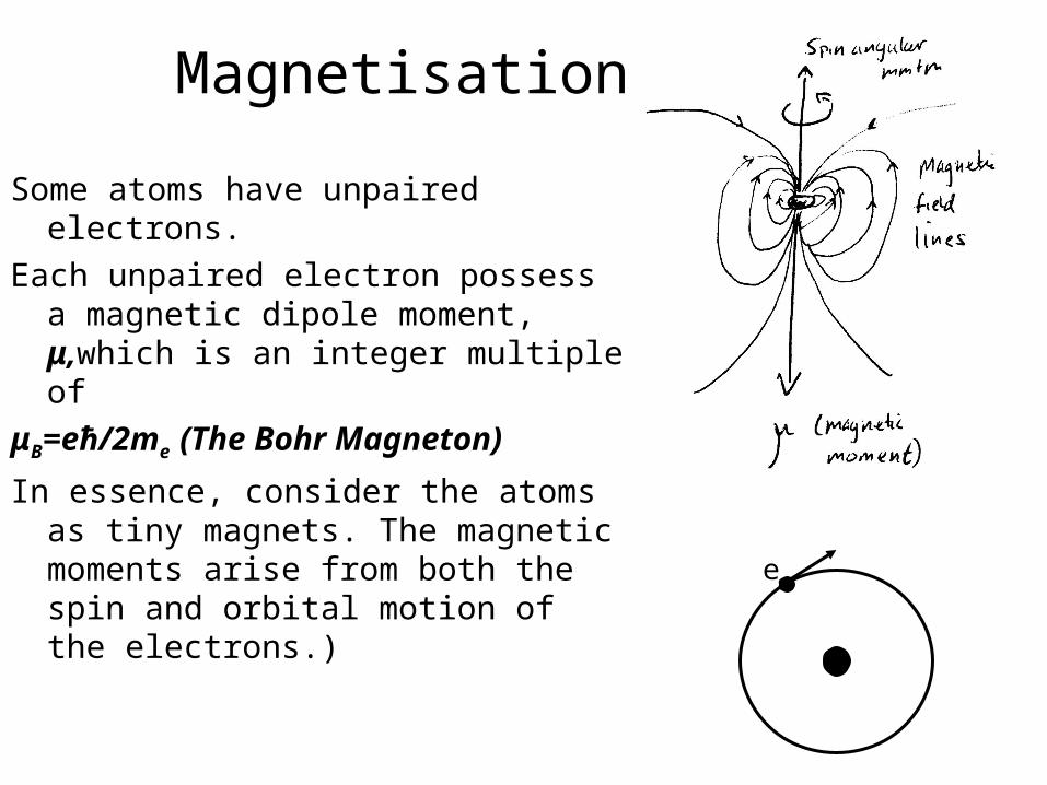
Some atoms have unpaired electrons.
Each unpaired electron possess a magnetic dipole moment, μ,which is an integer multiple of
μB=eħ/2me (The Bohr Magneton)
In essence, consider the atoms as tiny magnets. The magnetic moments arise from both the spin and orbital motion of the electrons.) e
Magnetisation
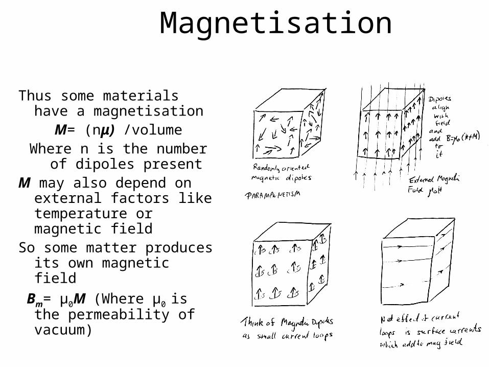
Thus some materials have a magnetisation
M= (nμ) /volumeWhere n is the number of
dipoles presentM may also depend on
external factors like temperature or magnetic field
So some matter produces its own magnetic field
Bm= μ0M (Where μ0 is the permeability of vacuum)
More magnetisation
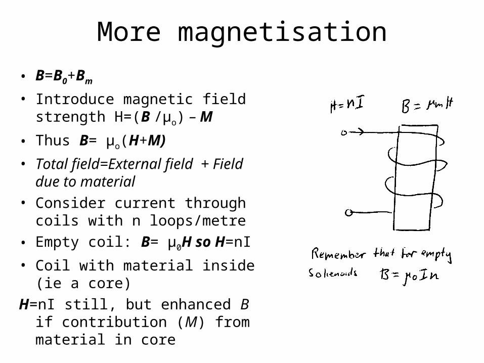
• B=B0+Bm
• Introduce magnetic field strength H=(B /μo) – M
• Thus B= μo(H+M)
• Total field=External field + Field due to material
• Consider current through coils with n loops/metre
• Empty coil: B= μ0H so H=nI
• Coil with material inside (ie a core)
H=nI still, but enhanced B if contribution (M) from material in core
Dia-, Para-, Ferro-,…• Magnetisation M depends on magnetic field
strength H via M=χHχ =magnetic susceptibility
• χ >0 =>paramagnetic (boosts applied field)
• χ <0 =>diamagnetic (reduces applied field)
Ferromagnetism can be thought of as an extreme case of paramagnetism with a variable χ (typically χ>>0 for Ferromagnetic material).
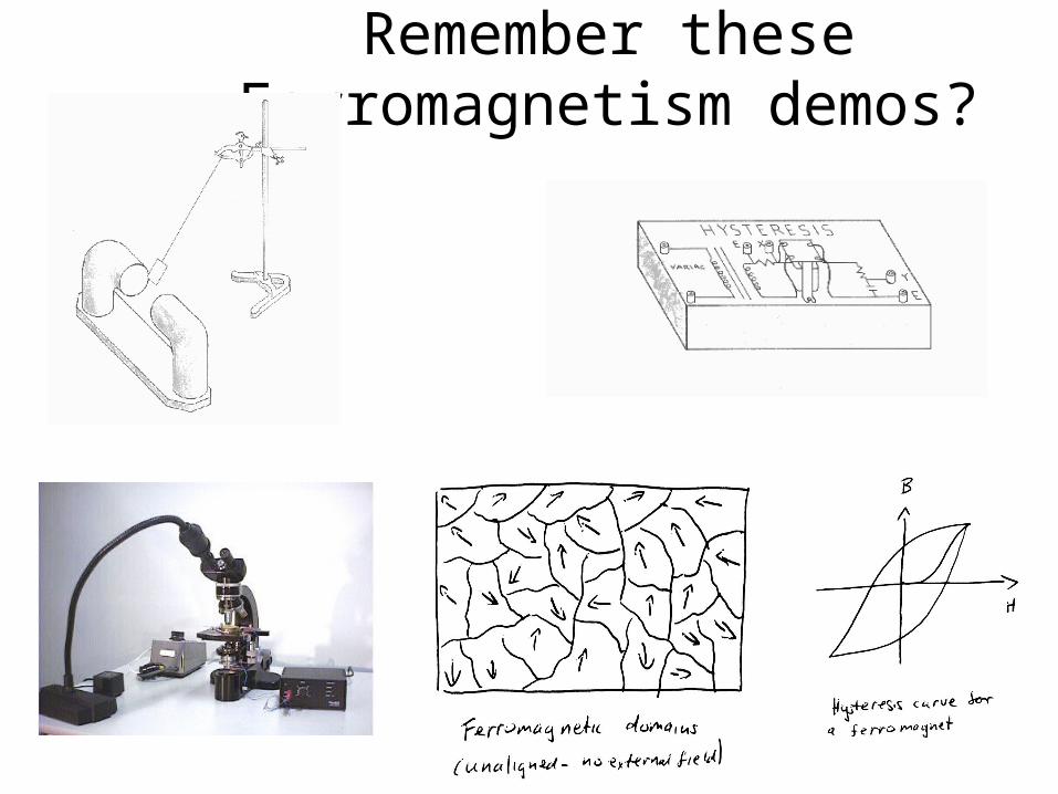
Remember these Ferromagnetism demos?
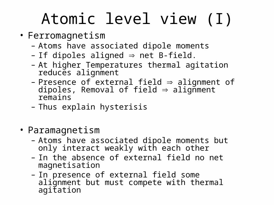
Atomic level view (I)• Ferromagnetism
– Atoms have associated dipole moments– If dipoles aligned net B-field.– At higher Temperatures thermal agitation reduces
alignment– Presence of external field alignment of dipoles,
Removal of field alignment remains– Thus explain hysterisis
• Paramagnetism– Atoms have associated dipole moments but only
interact weakly with each other – In the absence of external field no net magnetisation– In presence of external field some alignment but must
compete with thermal agitation
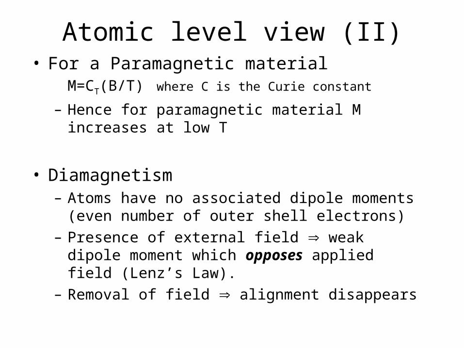
Atomic level view (II)• For a Paramagnetic material
M=CT(B/T) where C is the Curie constant
– Hence for paramagnetic material M increases at low T
• Diamagnetism– Atoms have no associated dipole moments (even
number of outer shell electrons)
– Presence of external field weak dipole moment which opposes applied field (Lenz’s Law).
– Removal of field alignment disappears

Superconductivity: A Historical introduction
• 1908: He first liquefied ( by Onnes)
• 1911:Observed that resistance of liquid Hg plummets at 4.2 K
• This ultra-low resistance termed superconductivity
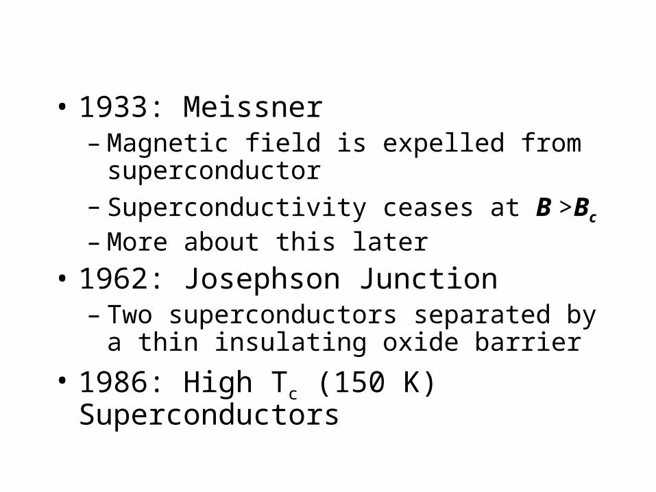
• 1933: Meissner– Magnetic field is expelled from superconductor– Superconductivity ceases at B >Bc
– More about this later
• 1962: Josephson Junction– Two superconductors separated by a thin
insulating oxide barrier
• 1986: High Tc (150 K) Superconductors
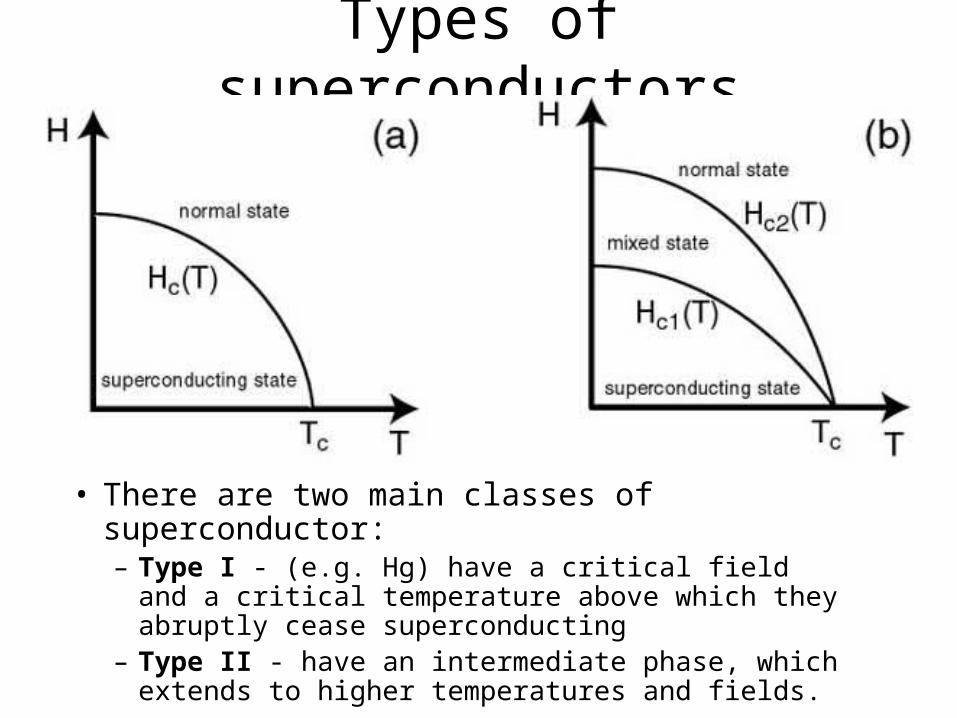
Types of superconductors
• There are two main classes of superconductor:– Type I - (e.g. Hg) have a critical field and a critical
temperature above which they abruptly cease superconducting
– Type II - have an intermediate phase, which extends to higher temperatures and fields.
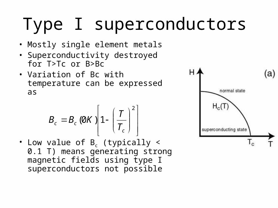
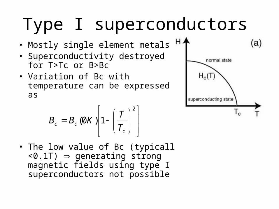
Type I superconductors• Mostly single element metals• Superconductivity destroyed for T>Tc
or B>Bc• Variation of Bc with temperature can
be expressed as
• Low value of Bc (typically < 0.1 T) means generating strong magnetic fields using type I superconductors not possible
2
1)0(c
cc T
TKBB
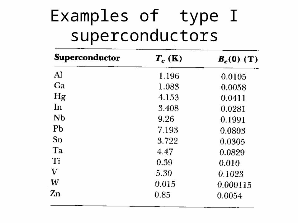
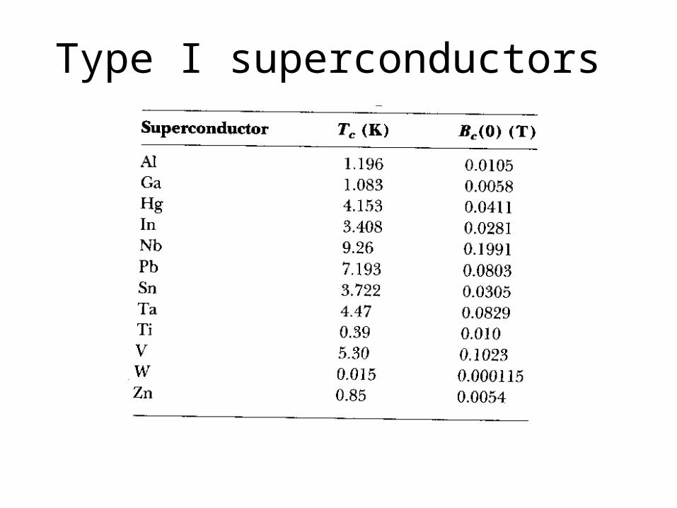
Examples of type I superconductors

Meissner Effect
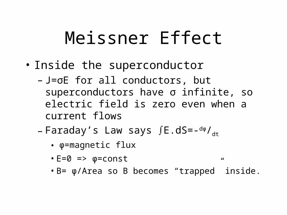
• Inside the superconductor– J=σE for all conductors, but superconductors
have σ infinite, so electric field is zero even when a current flows
– Faraday’s Law says ∫E.dS=-dφ/dt
where φ=magnetic flux• E=0 => φ=const
• B= φ/Area so B becomes “trapped” inside.
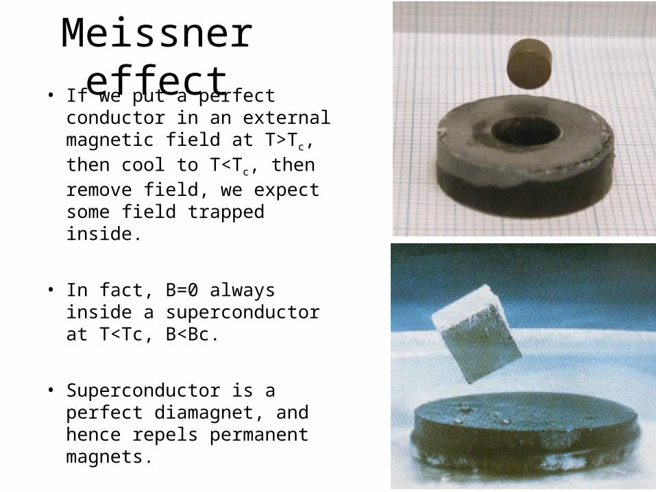
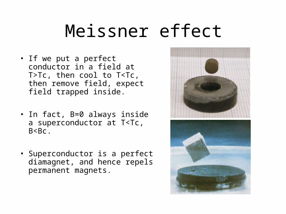
Meissner effect• If we put a perfect conductor in
an external magnetic field at T>Tc, then cool to T<Tc, then remove field, we expect some field trapped inside.
• In fact, B=0 always inside a superconductor at T<Tc, B<Bc.
• Superconductor is a perfect diamagnet, and hence repels permanent magnets.
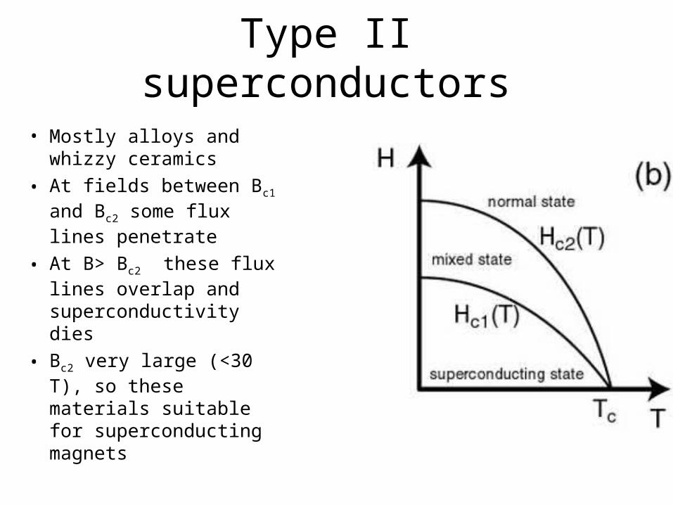
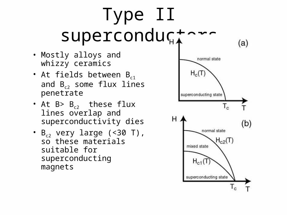
Type II superconductors
• Mostly alloys and whizzy ceramics
• At fields between Bc1 and Bc2 some flux lines penetrate
• At B> Bc2 these flux lines overlap and superconductivity dies
• Bc2 very large (<30 T), so these materials suitable for superconducting magnets
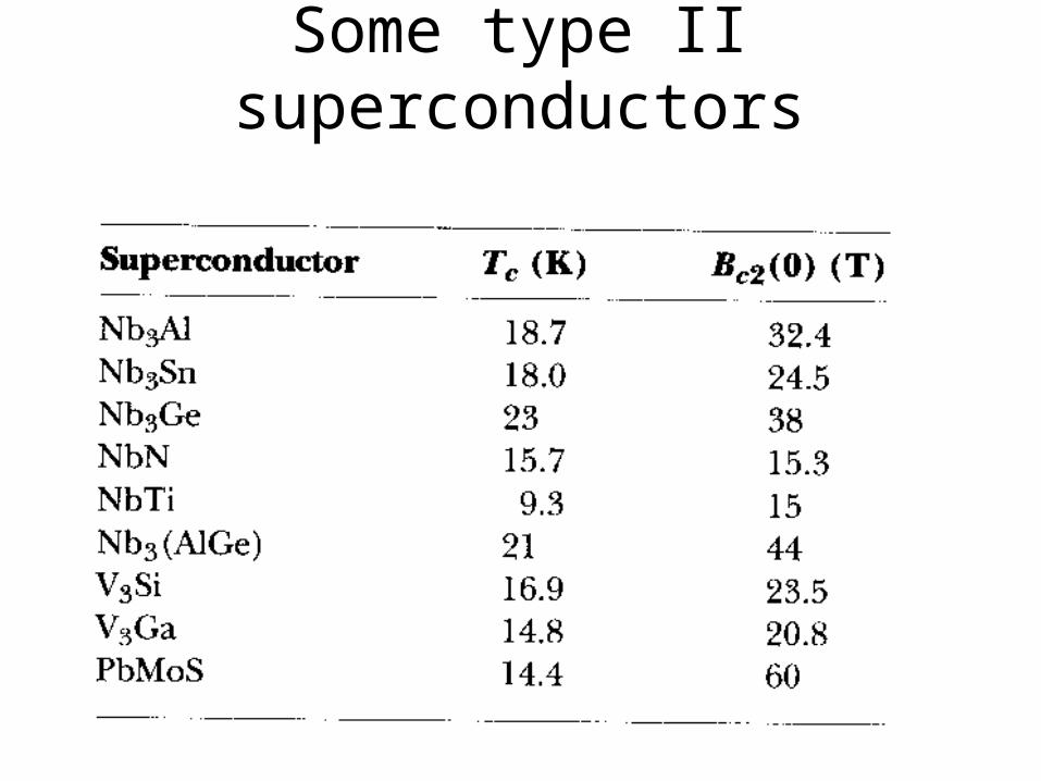
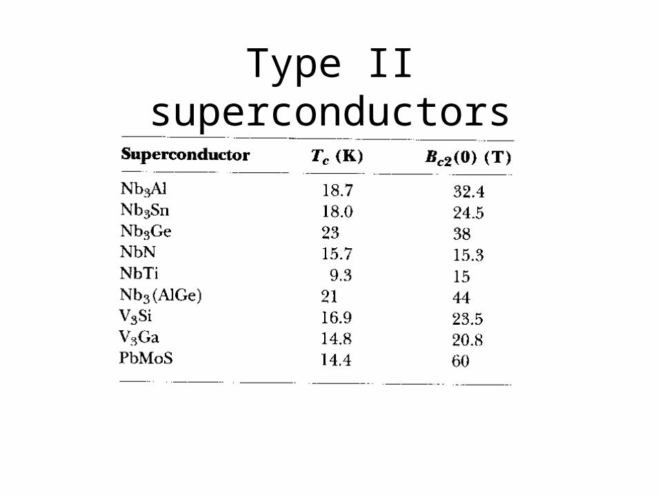
Some type II superconductors
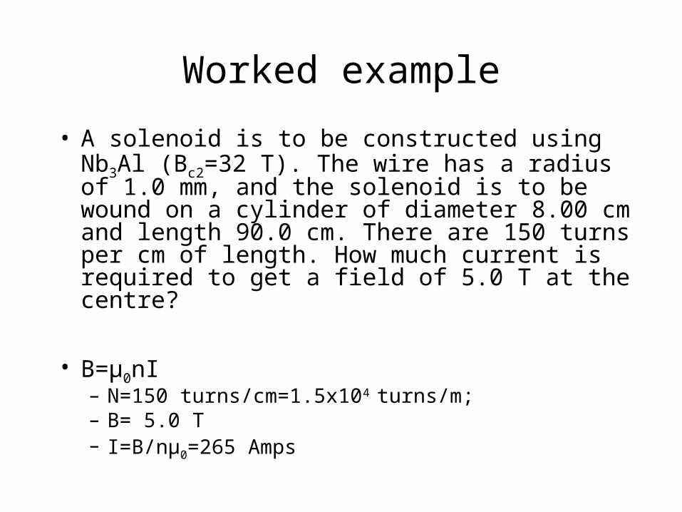
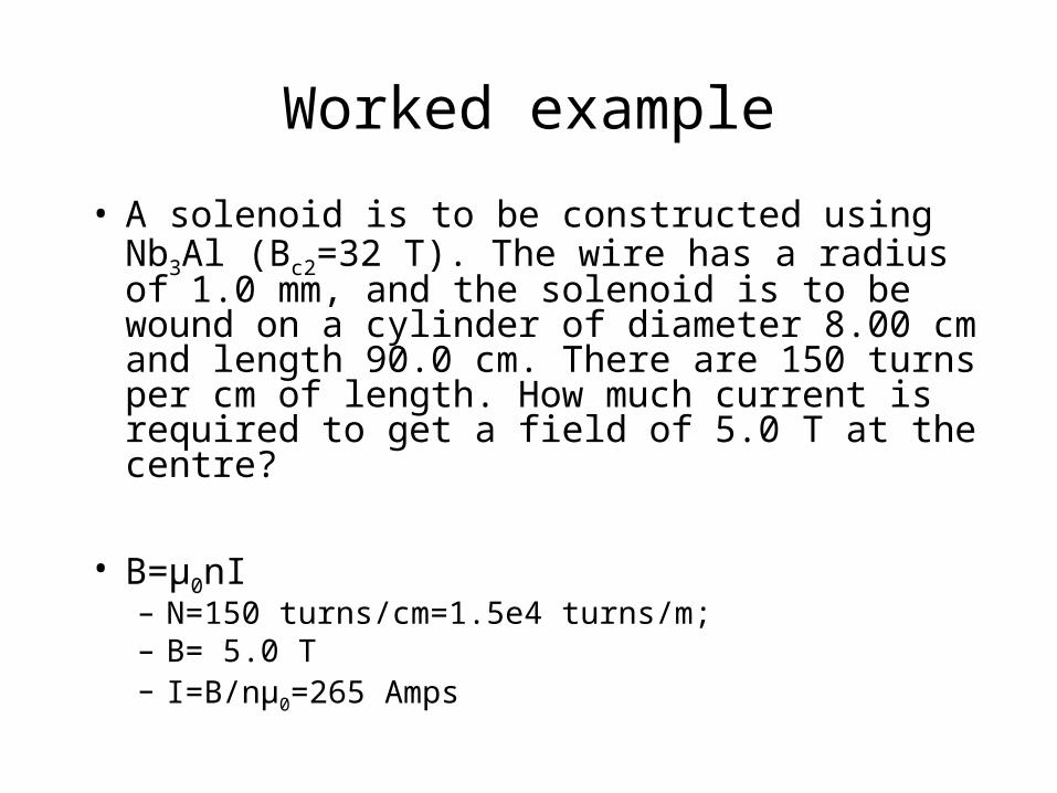
Worked example
• A solenoid is to be constructed using Nb3Al (Bc2=32 T). The wire has a radius of 1.0 mm, and the solenoid is to be wound on a cylinder of diameter 8.00 cm and length 90.0 cm. There are 150 turns per cm of length. How much current is required to get a field of 5.0 T at the centre?
• B=μ0nI– N=150 turns/cm=1.5x104 turns/m; – B= 5.0 T– I=B/nμ0=265 Amps

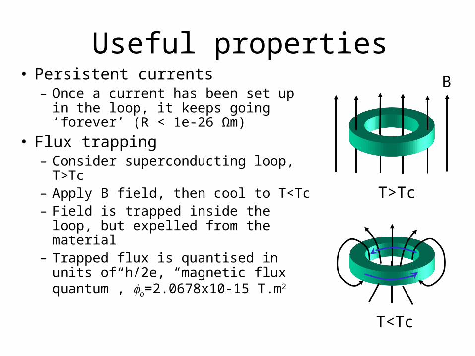
Useful properties• Persistent currents
– Once a current has been set up in the loop, it keeps going ‘forever’ (R < 1e-26 Ωm)
• Flux trapping– Consider superconducting loop, T>Tc– Apply B field, then cool to T<Tc– Field is trapped inside the loop, but
expelled from the material– Trapped flux is quantised in units of
h/2e, “magnetic flux quantum”, o=2.0678x10⁻¹⁵ T.m2
T>Tc
T<Tc
B
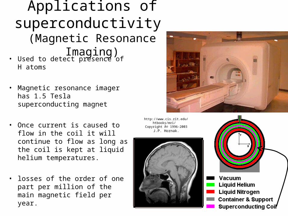
Applications of superconductivity (Magnetic
Resonance Imaging)
http://www.cis.rit.edu/htbooks/mri/ Copyright © 1996-2003 J.P.
Hornak.
• Used to detect presence of H atoms
• Magnetic resonance imager has 1.5 Tesla superconducting magnet
• Once current is caused to flow in the coil it will continue to flow as long as the coil is kept at liquid helium temperatures.
• losses of the order of one part per million of the main magnetic field per year.
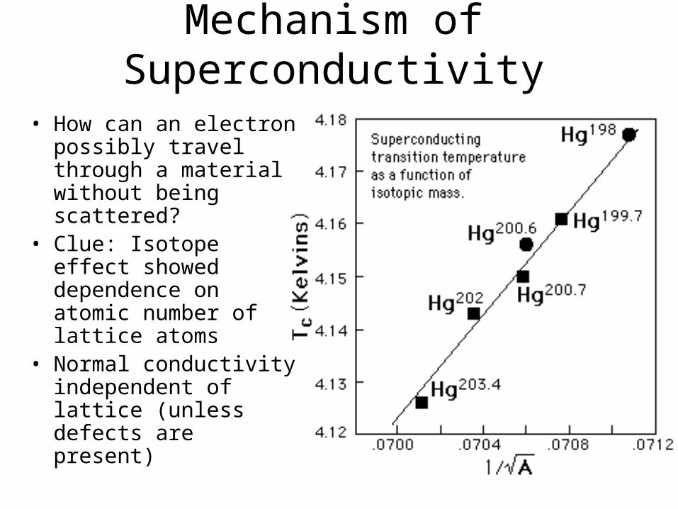
Mechanism of Superconductivity
• How can an electron possibly travel through a material without being scattered?
• Clue: Isotope effect showed dependence on atomic number of lattice atoms
• Normal conductivity independent of lattice (unless defects are present)
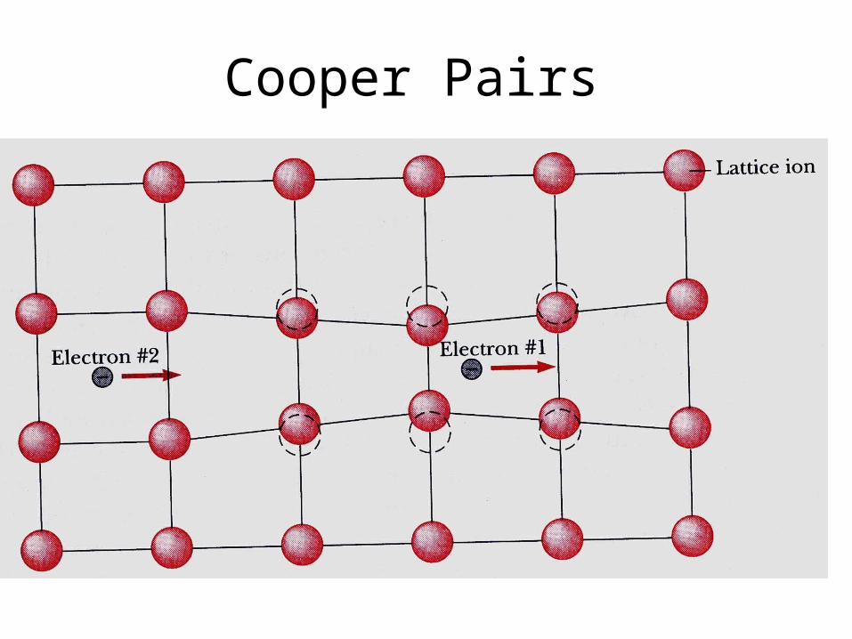
Cooper Pairs
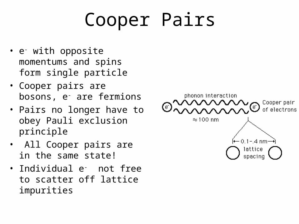
Cooper Pairs
• e- with opposite momentums and spins form single particle
• Cooper pairs are bosons, e- are fermions
• Pairs no longer have to obey Pauli exclusion principle
• All Cooper pairs are in the same state!
• Individual e- not free to scatter off lattice impurities
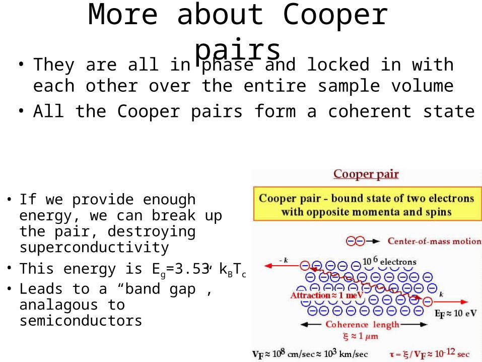
More about Cooper pairs
• If we provide enough energy, we can break up the pair, destroying superconductivity
• This energy is Eg=3.53 kBTc
• Leads to a “band gap”, analagous to semiconductors
• They are all in phase and locked in with each other over the entire sample volume
• All the Cooper pairs form a coherent state
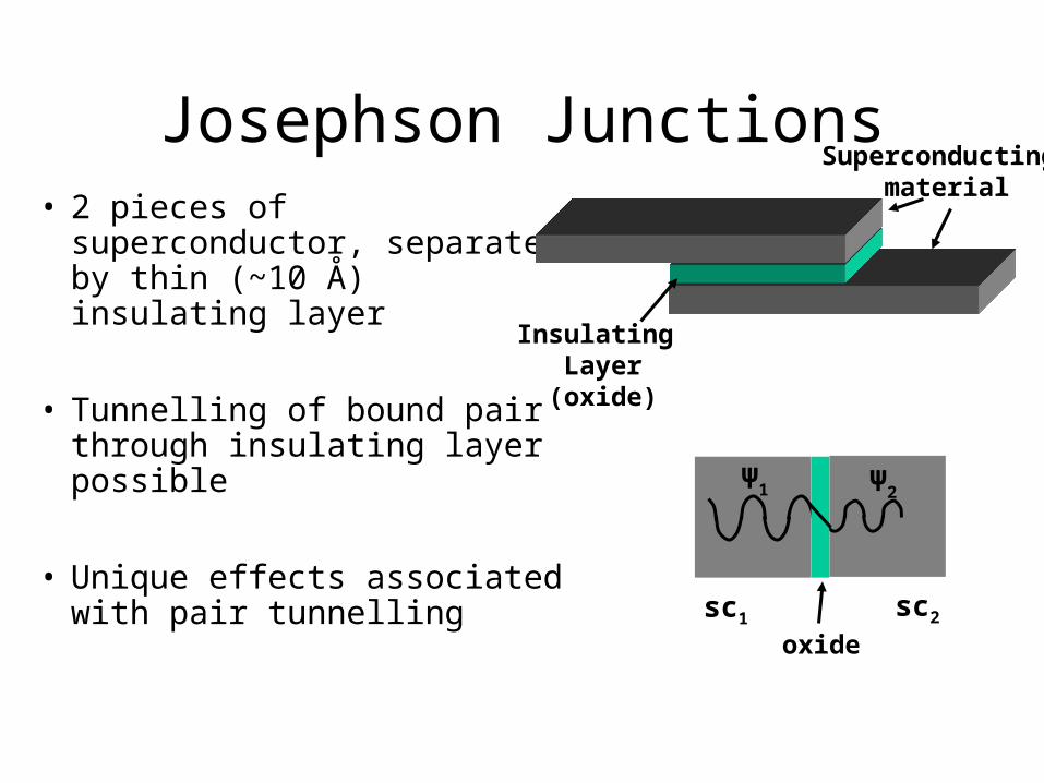
Josephson Junctions• 2 pieces of superconductor,
separated by thin (~10 Å) insulating layer
• Tunnelling of bound pair through insulating layer possible
• Unique effects associated with pair tunnelling
Superconducting material
Insulating Layer(oxide)
Ψ1 Ψ2
oxide
sc1 sc2

The DC Josephson effect
• At zero voltage there exists a superconducting current given by
Is=Imaxsin(φ1-φ2)=Imaxsin(δ)
• Imax is the maximum current across the junction under zero bias conditions
Dependant on thickness of insulating layer and junction
area
Phase difference between the wavefunctions in the two
superconductors

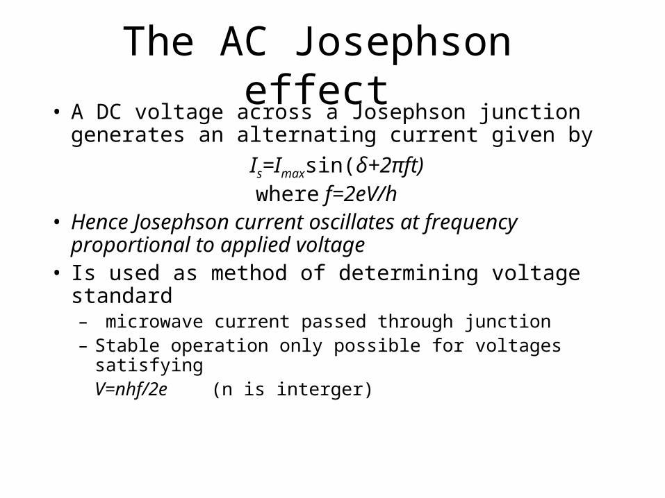
The AC Josephson effect• A DC voltage across a Josephson junction
generates an alternating current given by
Is=Imaxsin(δ+2πft)where f=2eV/h
• Hence Josephson current oscillates at frequency proportional to applied voltage
• Is used as method of determining voltage standard– microwave current passed through junction– Stable operation only possible for voltages satisfying
V=nhf/2e (n is interger)
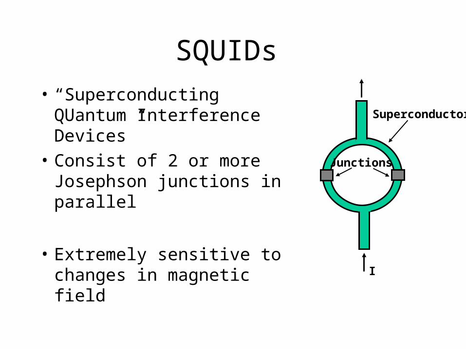
SQUIDs
• “Superconducting QUantum Interference Devices”
• Consist of 2 or more Josephson junctions in parallel
• Extremely sensitive to changes in magnetic field
Junctions
Superconductor
I
SQUIDs
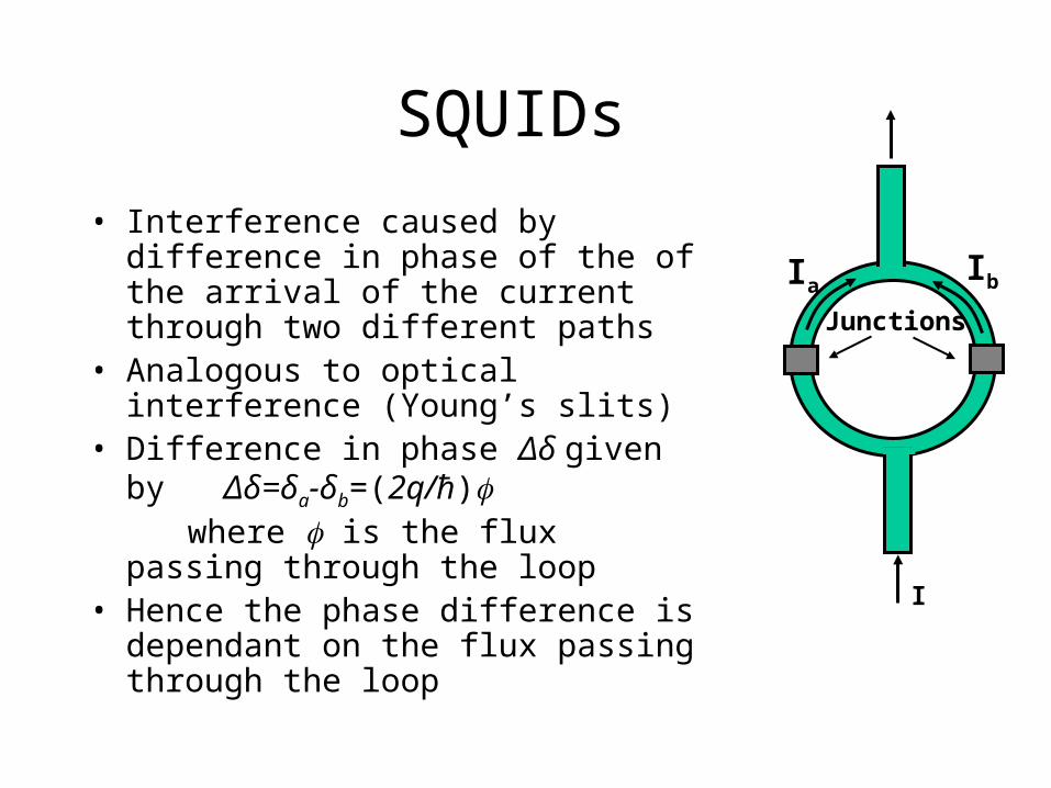
• Interference caused by difference in phase of the of the arrival of the current through two different paths
• Analogous to optical interference (Young’s slits)
• Difference in phase Δδ given by Δδ=δa-δb=(2q/ħ)
where is the flux passing through the loop
• Hence the phase difference is dependant on the flux passing through the loop
Junctions
I
IaIb
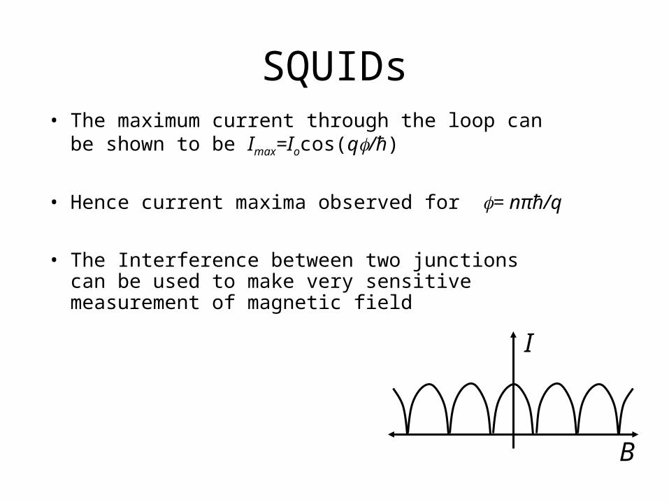
• The maximum current through the loop can be shown to be Imax=Iocos(q/ħ)
• Hence current maxima observed for = nπħ/q
• The Interference between two junctions can be used to make very sensitive measurement of magnetic field
SQUIDs
B
I
Applications of SQUIDs• Biomagnetism
– Some processes in animals/humans produce very small magnetic fields. The only type of detector sensitive enough to measure such a field is a SQUID.
– Magnetoencephalography (MEG) the imaging of the human brain. Involves measuring the magnetic field produced by the currents due to neural activity.
– Advantages other methods which only image the structure of the brain
• Non Destructive testing– Potential uses in monitoring internal faults or wear in
metal containing structures.
Lecture 24
History of Superconductivity
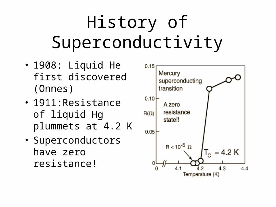
• 1908: Liquid He first discovered (Onnes)
• 1911:Resistance of liquid Hg plummets at 4.2 K
• Superconductors have zero resistance!
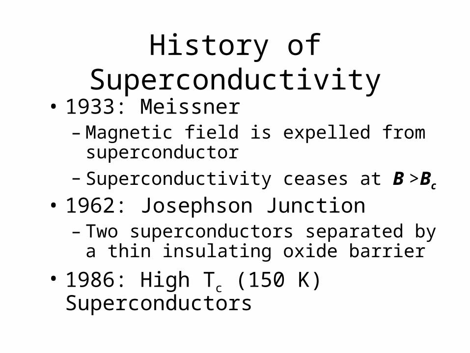
History of Superconductivity
• 1933: Meissner– Magnetic field is expelled from superconductor– Superconductivity ceases at B >Bc
• 1962: Josephson Junction– Two superconductors separated by a thin
insulating oxide barrier
• 1986: High Tc (150 K) Superconductors
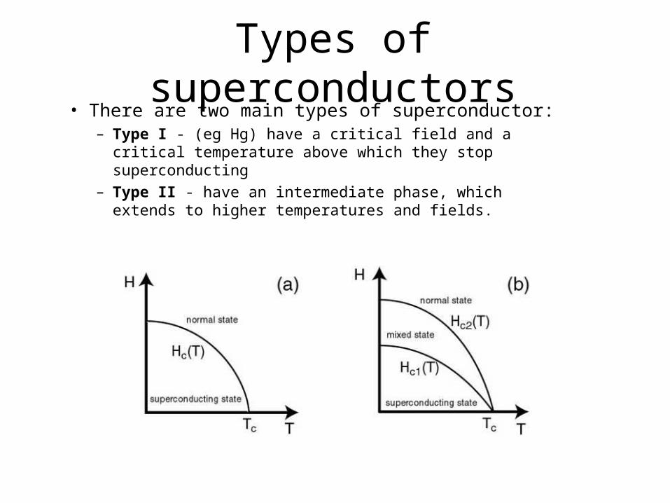
Types of superconductors• There are two main types of superconductor:
– Type I - (eg Hg) have a critical field and a critical temperature above which they stop superconducting
– Type II - have an intermediate phase, which extends to higher temperatures and fields.
Type I superconductors• Mostly single element metals• Superconductivity destroyed for T>Tc
or B>Bc• Variation of Bc with temperature can
be expressed as
• The low value of Bc (typicall <0.1T) generating strong magnetic fields using type I superconductors not possible
2
1)0(c
cc T
TKBB
Type I superconductors
Meissner Effect
• Inside the superconductor– J=σE for all conductors, but superconductors
have σ infinite, so electric field is zero even when a current flows
– Faraday’s Law says ∫E.dS=-dφ/dt
• φ=magnetic flux
• E=0 => φ=const
• B= φ/Area so B becomes “trapped” inside.
Meissner effect
• If we put a perfect conductor in a field at T>Tc, then cool to T<Tc, then remove field, expect field trapped inside.
• In fact, B=0 always inside a superconductor at T<Tc, B<Bc.
• Superconductor is a perfect diamagnet, and hence repels permanent magnets.
Type II superconductors
• Mostly alloys and whizzy ceramics
• At fields between Bc1 and Bc2 some flux lines penetrate
• At B> Bc2 these flux lines overlap and superconductivity dies
• Bc2 very large (<30 T), so these materials suitable for superconducting magnets
Type II superconductors
Worked example
• A solenoid is to be constructed using Nb3Al (Bc2=32 T). The wire has a radius of 1.0 mm, and the solenoid is to be wound on a cylinder of diameter 8.00 cm and length 90.0 cm. There are 150 turns per cm of length. How much current is required to get a field of 5.0 T at the centre?
• B=μ0nI– N=150 turns/cm=1.5e4 turns/m; – B= 5.0 T– I=B/nμ0=265 Amps
Useful properties• Persistent currents
– Once a current has been set up in the loop, it keeps going ‘forever’ (R < 1e-26 Ωm)
• Flux trapping– Consider superconducting loop, T>Tc– Apply B field, then cool to T<Tc– Field is trapped inside the loop, but
expelled from the material– Trapped flux is quantised in units of
h/2e, “magnetic flux quantum”, o=2.0678x10⁻¹⁵ T.m2
T>Tc
T<Tc
B
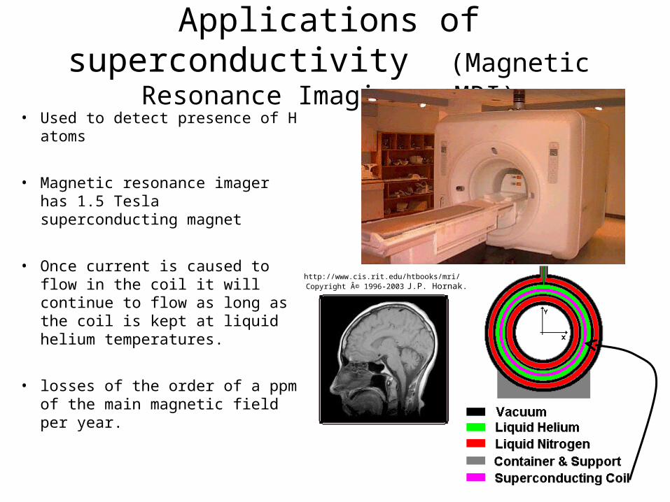
Applications of superconductivity (Magnetic Resonance Imaging – MRI)
http://www.cis.rit.edu/htbooks/mri/ Copyright © 1996-2003 J.P. Hornak.
• Used to detect presence of H atoms
• Magnetic resonance imager has 1.5 Tesla superconducting magnet
• Once current is caused to flow in the coil it will continue to flow as long as the coil is kept at liquid helium temperatures.
• losses of the order of a ppm of the main magnetic field per year.
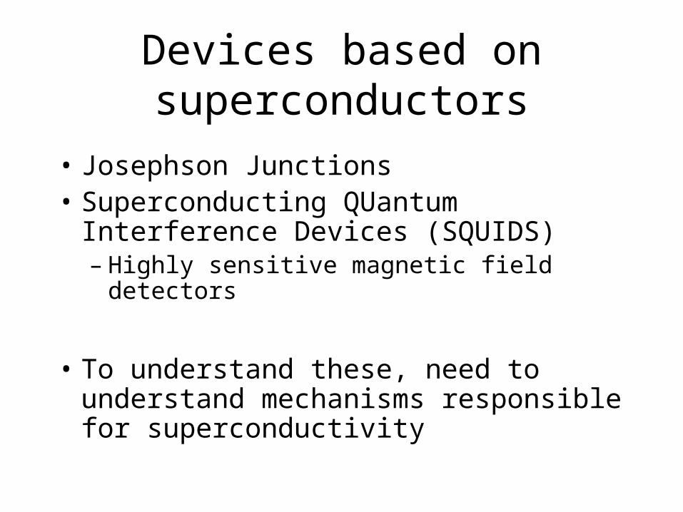
Devices based on superconductors
• Josephson Junctions• Superconducting QUantum Interference
Devices (SQUIDS)– Highly sensitive magnetic field detectors
• To understand these, need to understand mechanisms responsible for superconductivity
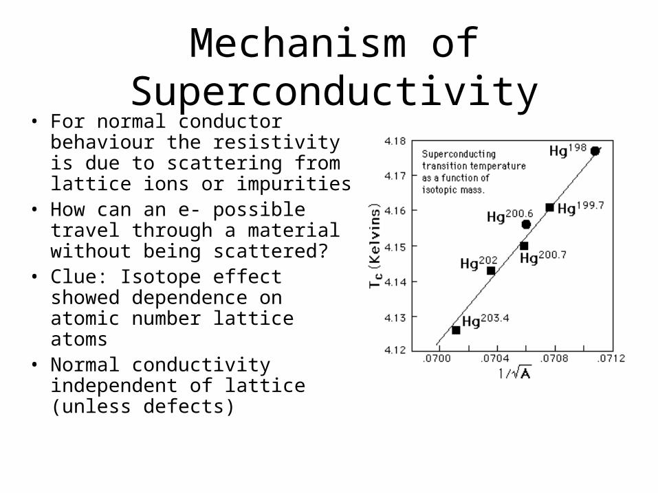
Mechanism of Superconductivity• For normal conductor behaviour
the resistivity is due to scattering from lattice ions or impurities
• How can an e- possible travel through a material without being scattered?
• Clue: Isotope effect showed dependence on atomic number lattice atoms
• Normal conductivity independent of lattice (unless defects)
Mechanism of Superconductivity• The features of superconductiviy can be explained using
theory developed by Bardeen, Cooper and Schrieffer (BCS theory)
• Main Features of BCS Theory– 2 electrons in a superconductor can form a bound pair via an
attractive interaction– known as a cooper pair
• How can negatively charged electrons form bound pair?– Net attraction possible if electron interact via motion of crystal
lattice
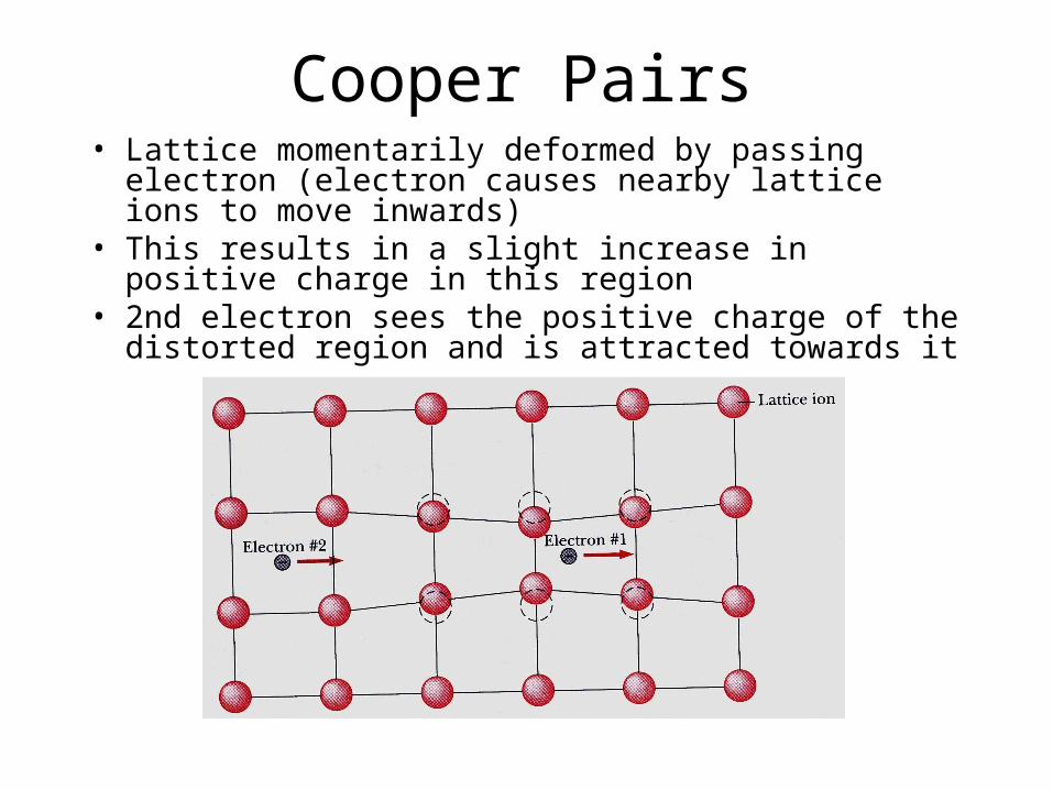
Cooper Pairs• Lattice momentarily deformed by passing electron
(electron causes nearby lattice ions to move inwards)• This results in a slight increase in positive charge in this
region• 2nd electron sees the positive charge of the distorted
region and is attracted towards it
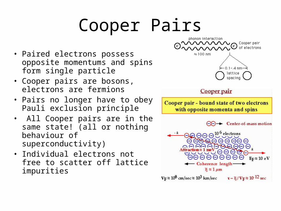
Cooper Pairs
• Paired electrons possess opposite momentums and spins form single particle
• Cooper pairs are bosons, electrons are fermions
• Pairs no longer have to obey Pauli exclusion principle
• All Cooper pairs are in the same state! (all or nothing behaviour of superconductivity)
• Individual electrons not free to scatter off lattice impurities
More Cooper pairs• All the cooper pairs form a coherent state• They are all in phase and locked in with each other
over the entire sample volume• If we provide enough energy, we can break up the
pair, destroying superconductivity
• This energy is Eg=3.53kBTc
• Leads to a “band gap”, analagous to semiconductors

Josephson Junctions• 2 pieces of superconductor,
separated by thin (~10 Å) insulating layer
• Tunnelling of bound pair through insulating layer possible
• Unique effects associated with pair tunnelling
Superconducting material
Insulating Layer(oxide)
Ψ1 Ψ2
oxide
sc1 sc2
The DC Josephson effect
• At zero voltage there exists a superconducting current given by
Is=Imaxsin(φ1-φ2)=Imaxsin(δ)
• Imax is the maximum current across the junction under zero bias conditions
Dependant on thickness of insulating layer and junction
area
Phase difference between the wavefunctions in the two
superconductors
The AC Josephson effect• A DC voltage across a Josephson junction
generates an alternating current given by
Is=Imaxsin(δ+2πft)where f=2eV/h
• Hence Josephson current oscillates at frequency proportional to applied voltage
• Is used as method of determining voltage standard– microwave current passed through junction– Stable operation only possible for voltages satisfying
V=nhf/2e (n is interger)

SQUIDs
• “Superconducting QUantum Interference Devices”
• Consist of 2 or more Josephson junctions in parallel
• Extremely sensitive to changes in magnetic field
Junctions
Superconductor
I

SQUIDs
• Interference caused by difference in phase of the of the arrival of the current through two different paths
• Analogous to optical interference (Young’s slits)
• Difference in phase Δδ given by Δδ=δa-δb=(2q/ħ)
where is the flux passing through the loop
• Hence the phase difference is dependant on the flux passing through the loop
Junctions
I
IaIb

• The maximum current through the loop can be shown to be Imax=Iocos(q/ħ)
• Hence current maxima observed for = nπħ/q
• The Interference between two junctions can be used to make very sensitive measurement of magnetic field
SQUIDs
B
I

Applications of SQUIDs• Biomagnetism
– Some processes in animals/humans produce very small magnetic fields. The only type of detector sensitive enough to measure such a field is a SQUID.
– Magnetoencephalography (MEG) the imaging of the human brain. Involves measuring the magnetic field produced by the currents due to neural activity.
– Advantages other methods which only image the structure of the brain
• Non Destructive testing– Potential uses in monitoring internal faults or wear in
metal containing structures.