SMCJ Series - jestek.com.cn
5
Unipolar Bipolar SMCJ Series 1 2 1 2 Cathode Anode 1 2 ● Case: SMC ● Terminals: Solderable per MIL-STD-750, Method 2026 ● Approx. Weight: 0.22g / 0.0077oz FEATURES SMC CIRCUIT DIAGRAM MECHANICAL DATA ● 1500W peak pulse power capability at 10/1000μs waveform, repetition rate (duty cycles):0.01% ● Excellent clamping capability ● Low incremental surge resistance ● Typical IR less than 1μA when VBR min>12V ● For surface mounted applications to optimize board space ● Low profle package ● Built-in strain relief ● Typical failure mode is short from over- specifed voltage or current ● Whisker test is conducted based on JEDEC JESD201A per its table 4a and 4c ● IEC-61000-4-2 ESD 30kV(Air), 30kV (Contact) ● ESD protection of data lines in accordance with IEC 61000-4-2 ● EFT protection of data lines in accordance with IEC 61000-4-4 ● Fast response time: typically less than 1.0ps from 0V to BV min ● Glass passivated chip junction ● High temperature to reflow soldering guaranteed: 260°C/40sec ● VBR @ TJ= VBR@25°C x (1+αT x (TJ - 25))(αT:Temperature Coeffcient, typical value is 0.1%) ● Plastic package is flammability rated V-0 per Underwriters Laboratories ● Meet MSL level1, per J-STD-020, LF maximun peak of 260°C ● Matte tin lead–free plated ● Halogen free and RoHS compliant ● Pb-free E3 means 2nd level interconnect is Pb-free and the terminal fnish material is tin(Sn) (IPC/JEDEC J-STD-609A.01) Version:3 1/5
Transcript of SMCJ Series - jestek.com.cn
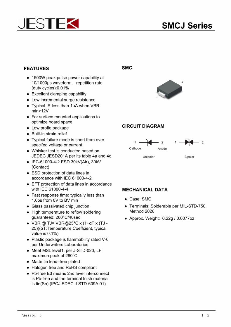
Unipolar Bipolar
SMCJ Series
1
2
1 2
Cathode Anode
1 2
● Case: SMC● Terminals: Solderable per MIL-STD-750,
Method 2026● Approx. Weight: 0.22g / 0.0077oz
FEATURES SMC
CIRCUIT DIAGRAM
MECHANICAL DATA
● 1500W peak pulse power capability at10/1000μs waveform, repetition rate(duty cycles):0.01%
● Excellent clamping capability● Low incremental surge resistance● Typical IR less than 1μA when VBR
min>12V● For surface mounted applications to
optimize board space● Low profle package● Built-in strain relief● Typical failure mode is short from over-
specifed voltage or current● Whisker test is conducted based on
JEDEC JESD201A per its table 4a and 4c● IEC-61000-4-2 ESD 30kV(Air), 30kV
(Contact)● ESD protection of data lines in
accordance with IEC 61000-4-2● EFT protection of data lines in accordance
with IEC 61000-4-4● Fast response time: typically less than
1.0ps from 0V to BV min● Glass passivated chip junction● High temperature to reflow soldering
guaranteed: 260°C/40sec● VBR @ TJ= VBR@25°C x (1+αT x (TJ -
25))(αT:Temperature Coeffcient, typicalvalue is 0.1%)
● Plastic package is flammability rated V-0per Underwriters Laboratories
● Meet MSL level1, per J-STD-020, LFmaximun peak of 260°C
● Matte tin lead–free plated● Halogen free and RoHS compliant● Pb-free E3 means 2nd level interconnect
is Pb-free and the terminal fnish materialis tin(Sn) (IPC/JEDEC J-STD-609A.01)
Version:3 1/5
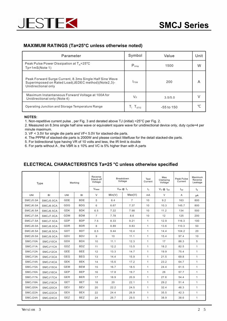
Parameter Symbol Value Unit
PPPM 1500 W
Peak Forward Surge Current, 8.3ms Single Half Sine Wave Superimposed on Rated Load(JEDEC method)(Note2,3)-Unidirectional only
IFSM 200
Maximum Instantaneous Forward Voltage at 100A for Unidirectional only (Note 4)
VF
A
V
Operating Junction and Storage Temperature Range T j TSTG -55 to 150 ℃
°C Peak Pulse Power Dissipation at TA=25
Tp=1mS(Note 1)
3.5/5.0
SMCJ Series
NOTES:1. Non-repetitive current pulse , per Fig. 3 and derated above TJ (initial) =25°C per Fig. 2.2. Measured on 8.3ms single half sine wave or equivalent square wave for unidirectional device only, duty cycle=4 perminute maximum.3. VF < 3.5V for single die parts and VF< 5.0V for stacked-die parts.4. The PPPM of stacked-die parts is 2000W and please contact littelfuse for the detail stacked-die parts.5. For bidirectional type having VR of 10 volts and less, the IR limit is double6. For parts without A , the VBR is ± 10% and VC is 5% higher than with A parts
Type
ReverseStand-offVoltage
BreakdownVoltage
VRMW VBR @ IT
Min(V) Max(V) A
TestCurrent
Max ClampingVoltage
Peak PulseCurrent
IT
mA
VC @ IPP IPP
UNI BI μA
Marking
SMCJ5.0A
SMCJ6.0A
SMCJ6.5A
SMCJ7.0A
SMCJ7.5A
SMCJ8.0A
SMCJ8.5A
SMCJ9.0A
SMCJ10A
SMCJ11A
SMCJ12A
SMCJ13A
SMCJ14A
SMCJ15A
SMCJ16A
SMCJ17A
SMCJ18A
SMCJ20A
SMCJ22A
SMCJ24A
SMCJ5.0CA
SMCJ6.0CA
SMCJ6.5CA
SMCJ7.0CA
SMCJ7.5CA
SMCJ8.0CA
SMCJ8.5CA
SMCJ9.0CA
SMCJ10CA
SMCJ11CA
SMCJ12CA
SMCJ13CA
SMCJ14CA
SMCJ15CA
SMCJ16CA
SMCJ17CA
SMCJ18CA
SMCJ20CA
SMCJ22CA
SMCJ24CA
GDE
GDG
GDK
GDM
GDP
GDR
GDT
GDV
GDX
GDZ
GEE
GEG
GEK
GEM
GEP
GER
GET
GEV
GEX
GEZ
BDE
BDG
BDK
BDM
BDP
BDR
BDT
BDV
BDX
BDZ
BEE
BEG
BEK
BEM
BEP
BER
BET
BEV
BEX
BEZ
Maximum Reverse Leakage
UNI BI V
IR
V
5
6
6.5
7
7.5
8
8.5
9
10
11
12
13
14
15
16
17
18
20
22
24
6.4
6.67
7.22
7.78
8.33
8.89
9.44
10
11.1
12.2
13.3
14.4
15.6
16.7
17.8
18.9
20
22.2
24.4
26.7
7
7.37
7.98
8.6
9.21
9.83
10.4
11.1
12.3
13.5
14.7
15.9
17.2
18.5
19.7
20.9
22.1
24.5
26.9
29.5
10
10
10
10
1
1
1
1
1
1
1
1
1
1
1
1
1
1
1
1
9.2
10.3
11.2
12
12.9
13.6
14.4
15.4
17
18.2
19.9
21.5
23.2
24.4
26
27.6
29.2
32.4
35.5
38.9
163
145.7
134
125
116.3
110.3
104.2
97.4
88.3
82.5
75.4
69.8
64.7
61.5
57.7
54.4
51.4
46.3
42.3
38.6
800
800
500
200
100
50
20
10
5
1
1
1
1
1
1
1
1
1
1
1
MAXIMUM RATINGS (Ta=25°C unless otherwise noted)
ELECTRICAL CHARACTERISTICS Ta=25 °C unless otherwise specified
Version:3 2/5
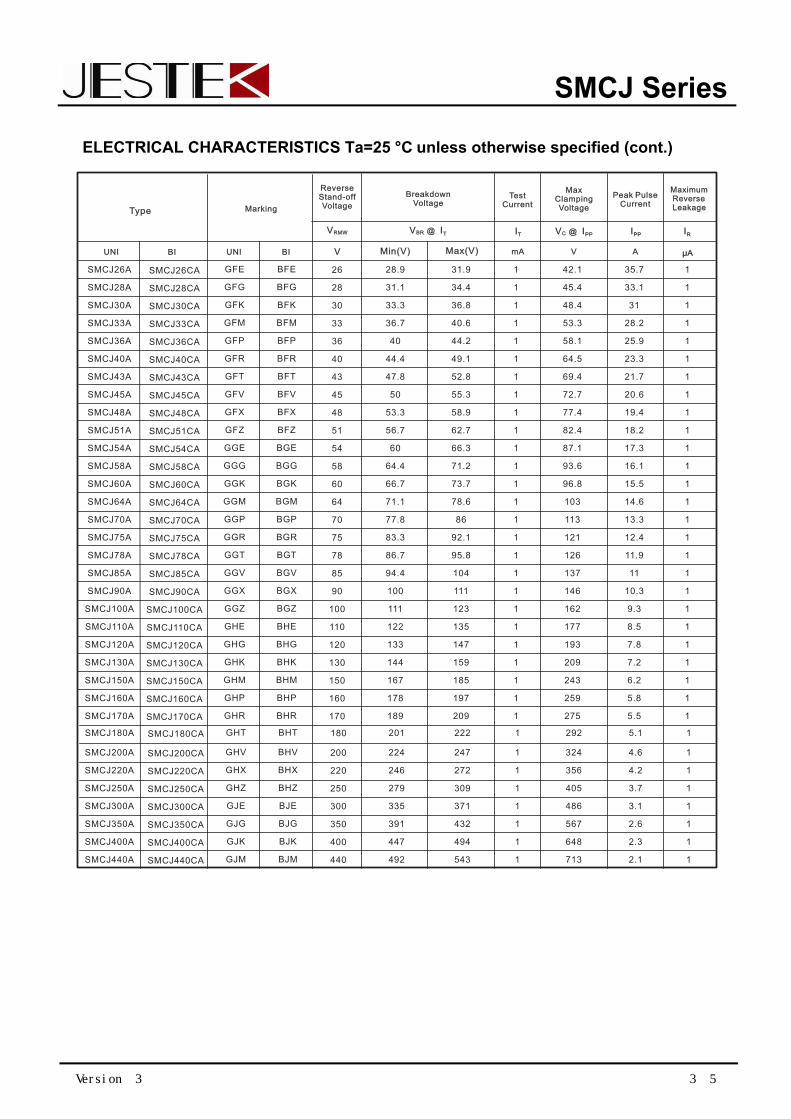
Type
ReverseStand-offVoltage
BreakdownVoltage
VRMW VBR @ IT
Min(V) Max(V) A
TestCurrent
Max ClampingVoltage
Peak PulseCurrent
IT
mA
VC @ IPP IPP
UNI BI μA
Marking
SMCJ26A
SMCJ28A
SMCJ30A
SMCJ33A
SMCJ36A
SMCJ40A
SMCJ43A
SMCJ45A
SMCJ48A
SMCJ51A
SMCJ54A
SMCJ58A
SMCJ60A
SMCJ64A
SMCJ70A
SMCJ75A
SMCJ78A
SMCJ85A
SMCJ90A
SMCJ100A
SMCJ110A
SMCJ120A
SMCJ130A
SMCJ150A
SMCJ160A
SMCJ170A
SMCJ26CA
SMCJ28CA
SMCJ30CA
SMCJ33CA
SMCJ36CA
SMCJ40CA
SMCJ43CA
SMCJ45CA
SMCJ48CA
SMCJ51CA
SMCJ54CA
SMCJ58CA
SMCJ60CA
SMCJ64CA
SMCJ70CA
SMCJ75CA
SMCJ78CA
SMCJ85CA
SMCJ90CA
SMCJ100CA
SMCJ110CA
SMCJ120CA
SMCJ130CA
SMCJ150CA
SMCJ160CA
SMCJ170CA
GFE
GFG
GFK
GFM
GFP
GFR
GFT
GFV
GFX
GFZ
GGE
GGG
GGK
GGM
GGP
GGR
GGT
GGV
GGX
GGZ
GHE
GHG
GHK
GHM
GHP
GHR
BFE
BFG
BFK
BFM
BFP
BFR
BFT
BFV
BFX
BFZ
BGE
BGG
BGK
BGM
BGP
BGR
BGT
BGV
BGX
BGZ
BHE
BHG
BHK
BHM
BHP
BHR
Maximum Reverse Leakage
UNI BI V
IR
V
26
28
30
33
36
40
43
45
48
51
54
58
60
64
70
75
78
85
90
100
110
120
130
150
160
170
28.9
31.1
33.3
36.7
40
44.4
47.8
50
53.3
56.7
60
64.4
66.7
71.1
77.8
83.3
86.7
94.4
100
111
122
133
144
167
178
189
31.9
34.4
36.8
40.6
44.2
49.1
52.8
55.3
58.9
62.7
66.3
71.2
73.7
78.6
86
92.1
95.8
104
111
123
135
147
159
185
197
209
1
1
1
1
1
1
1
1
1
1
1
1
1
1
1
1
1
1
1
1
1
1
1
1
1
1
42.1
45.4
48.4
53.3
58.1
64.5
69.4
72.7
77.4
82.4
87.1
93.6
96.8
103
113
121
126
137
146
162
177
193
209
243
259
275
35.7
33.1
31
28.2
25.9
23.3
21.7
20.6
19.4
18.2
17.3
16.1
15.5
14.6
13.3
12.4
11.9
11
10.3
9.3
8.5
7.8
7.2
6.2
5.8
5.5
1
1
1
1
1
1
1
1
1
1
1
1
1
1
1
1
1
1
1
1
1
1
1
1
1
1
SMCJ Series
SMCJ200A
SMCJ220A
SMCJ250A
SMCJ300A
SMCJ200CA
SMCJ220CA
SMCJ250CA
SMCJ300CA
GHV
GHX
GHZ
GJE
BHV
BHX
BHZ
BJE
200
220
250
300
224
246
279
335
247
272
309
371
1
1
1
1
324
356
405
486
4.6
4.2
3.7
3.1
1
1
1
1
SMCJ350A
SMCJ400A
SMCJ440A
SMCJ350CA
SMCJ400CA
SMCJ440CA
GJG
GJK
GJM
BJG
BJK
BJM
350
400
440
391
447
492
432
494
543
1
1
1
567
648
713
2.6
2.3
2.1
1
1
1
SMCJ180A SMCJ180CA GHT BHT 180 201 222 1 292 5.1 1
ELECTRICAL CHARACTERISTICS Ta=25 °C unless otherwise specified (cont.)
Version:3 3/5
20
40
60
80
100
025 50 75 100 125 150 175
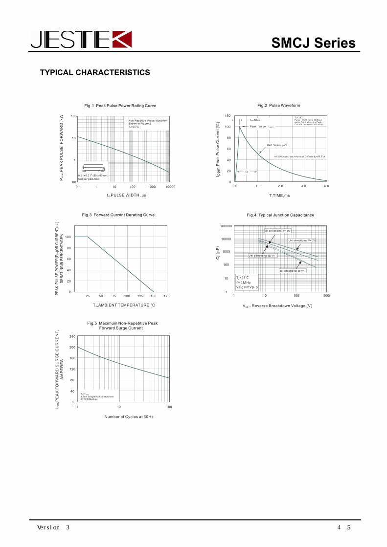
Fig.3 Forward Current Derating Curve
Fig.5 Maximum Non-Repetitive Peak Forward Surge Current
10 1001
0
40
80
120
200
160
240
I,P
EA
K F
OR
WA
RD
SU
RG
E C
UR
RE
NT,
FS
M
AM
PE
RE
S
Number of Cycles at 60Hz
PE
AK P
UL
SE P
OW
ER
(P)O
R C
UR
RE
NT
(I)
PP
PP
DE
RA
TIN
GIN
PE
RC
EN
TAG
E%
T ,AMBIENT TEMPERATURE,A °C
20
40
60
80
100
0
Fig.2 Pulse Waveform
0 1.0 2.0 3.0 4.0
150
I,P
ea
k P
uls
e C
urr
en
t (%
)p
pm
T,TIME,ms
Peak Value Ippm
Half Value-Ipp/2
10/1000usec Waveform as Defined bye R.E.A.
Pulse Width (td) is Definedas the Point where the Peak.Current Decayst to 50% of Ipp
TA=25
°Ct =10us f
TJ=TJmax 8.3ms Single Half Sinepwave JEDEC Method
Fig.1 Peak Pulse Power Rating Curve
10.1
00
1
10
100
10 100 1000 10000
P,P
EA
K P
UL
SE
F
OR
WA
RD
,kW
PP
M
t ,PULSE WIDTH ,usd
Non-Repetive Pulse.WavefomShown in Figure.3
T =25A °C
0.31x0.31" (80 x 80mm)
Copper pad Area
Uni-directional @ VR
Uni-directional V=0V
Bi-directional V= 0V
Bi-directional @ VR
Fig.4 Typical Junction Capacitance
1
1000
10000
100000
10
100
Cj (p
F)
1 10 100 1000
V - Reverse Breakdown Voltage (V)BR
td
Tj=25℃
f=1MHz
Vsig=mVp-p
SMCJ Series
TYPICAL CHARACTERISTICS
Version:3 4/5
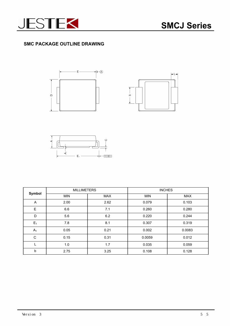
SMCJ Series
D
E1 AV M
A C
E A
b
L
A1
Symbol MILLIMETERS INCHES
MIN MAX MIN MAX
A 2.00 2.62 0.079 0.103
E 6.6 7.1 0.260 0.280
D 5.6 6.2 0.220 0.244
E1 7.8 8.1 0.307 0.319
A1 0.05 0.21 0.002 0.0083
L
b
1.0 1.7 0.035 0.059
C 0.15 0.31 0.0059 0.012
2.75 3.25 0.108 0.128
SMC PACKAGE OUTLINE DRAWING
Version:3 5/5