AC Servo Drives V Series/ V Series for Large-Capacity Models
RM590L Series
400mA Synchronous Step-down DC/DC Module with MODE pin and Inductor
No.EA-592-210906
1
0102030405060708090
100
0.01 0.1 1 10 100 1000
Effic
ienc
y η
[%]
Output Current IOUT [mA]
VIN = 2.7VVIN = 3.6VVIN = 4.2VVIN = 5.0V
VIN = 2.7V VIN = 3.6VVIN = 4.2VVIN = 5.0V
VFM / PWM Auto
Forced PWMVIN = 3.6V
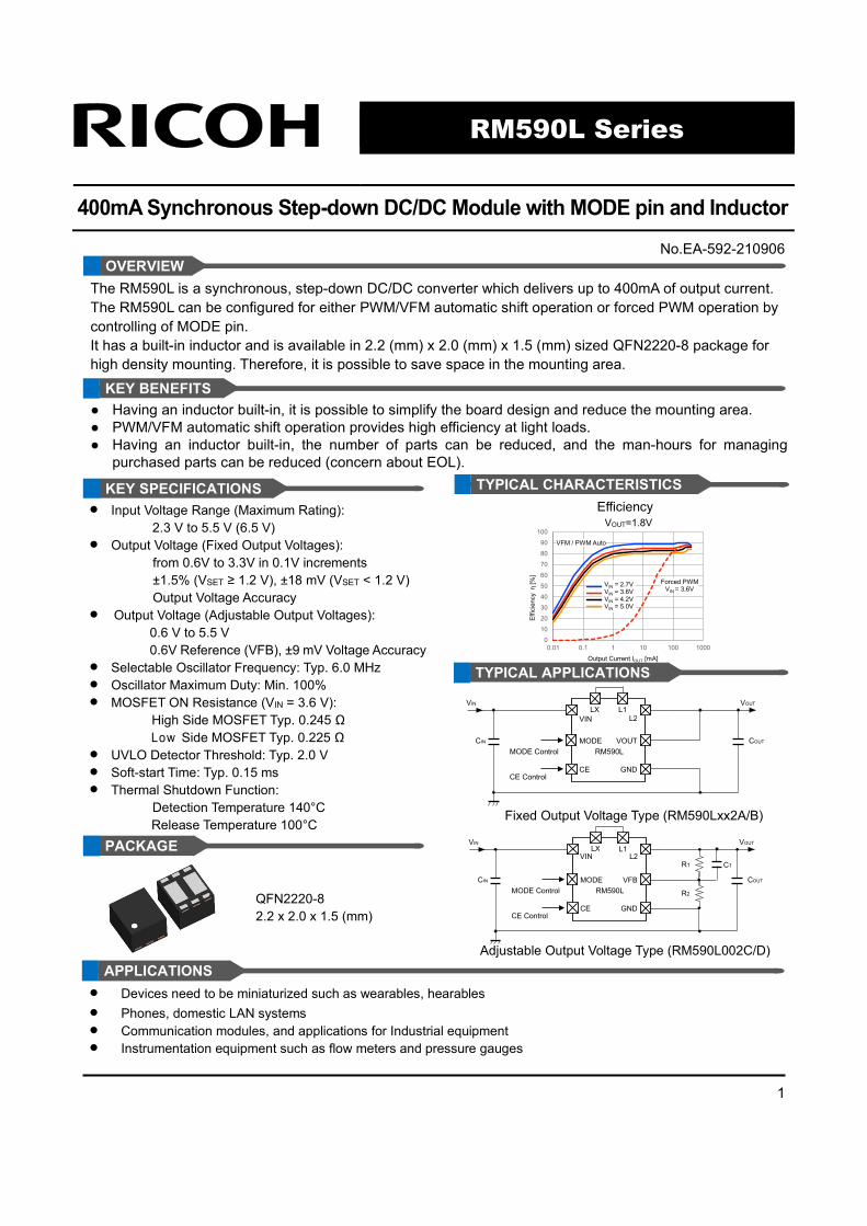
The RM590L is a synchronous, step-down DC/DC converter which delivers up to 400mA of output current. The RM590L can be configured for either PWM/VFM automatic shift operation or forced PWM operation by controlling of MODE pin. It has a built-in inductor and is available in 2.2 (mm) x 2.0 (mm) x 1.5 (mm) sized QFN2220-8 package for high density mounting. Therefore, it is possible to save space in the mounting area. Having an inductor built-in, it is possible to simplify the board design and reduce the mounting area. PWM/VFM automatic shift operation provides high efficiency at light loads. Having an inductor built-in, the number of parts can be reduced, and the man-hours for managing
purchased parts can be reduced (concern about EOL). • Input Voltage Range (Maximum Rating):
2.3 V to 5.5 V (6.5 V) • Output Voltage (Fixed Output Voltages):
from 0.6V to 3.3V in 0.1V increments ±1.5% (VSET ≥ 1.2 V), ±18 mV (VSET < 1.2 V) Output Voltage Accuracy
• Output Voltage (Adjustable Output Voltages): 0.6 V to 5.5 V 0.6V Reference (VFB), ±9 mV Voltage Accuracy
• Selectable Oscillator Frequency: Typ. 6.0 MHz • Oscillator Maximum Duty: Min. 100% • MOSFET ON Resistance (VIN = 3.6 V):
High Side MOSFET Typ. 0.245 Ω Low Side MOSFET Typ. 0.225 Ω
• UVLO Detector Threshold: Typ. 2.0 V • Soft-start Time: Typ. 0.15 ms • Thermal Shutdown Function:
Detection Temperature 140°C Release Temperature 100°C
Efficiency
Fixed Output Voltage Type (RM590Lxx2A/B)
Adjustable Output Voltage Type (RM590L002C/D)
QFN2220-8 2.2 x 2.0 x 1.5 (mm)
• Devices need to be miniaturized such as wearables, hearables • Phones, domestic LAN systems • Communication modules, and applications for Industrial equipment • Instrumentation equipment such as flow meters and pressure gauges
KEY BENEFITS
KEY SPECIFICATIONS TYPICAL CHARACTERISTICS
TYPICAL APPLICATIONS
PACKAGE
APPLICATIONS
OVERVIEW
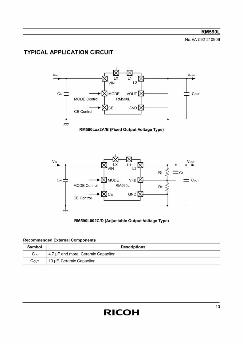
VIN
CE
L2
VOUT
GND
VIN
CIN COUT
VOUT
RM590L MODE
LX L1
MODE Control
CE Control
VIN
CE
L2
VFB
GND
VIN
CIN COUT
VOUT
RM590L MODE
LX L1
R2
C1 R1
MODE Control
CE Control
VOUT=1.8V
RM590L No.EA-592-210906
2
SELECTION GUIDE The set output voltage, the output voltage type, and the auto-discharge function are user-selectable options.
Selection Guide Product Name Package Quantity per Reel Pb Free Halogen Free
RM590Lxx2$-TR QFN2220-8 2,000 Yes Yes
xx:Set Output Voltage (VSET) Fixed Output Voltage Type:06 to 33 (0.6 V to 3.3 V, 0.1 V steps)
The voltage in 0.05 V step is shown as follows. Ex. 1.25 V: RM590L122$5 Refer to Product-specific Electrical Characteristics for details.
Adjustable Output Voltage Type:00 $ :Versions
$ Output Voltage Type Auto-discharge Function VSET A
Fixed No
0.6 V to 3.3 V B Yes C
Adjustable No
0.6 V to 5.5 V D Yes
RM590L No.EA-592-210906
3
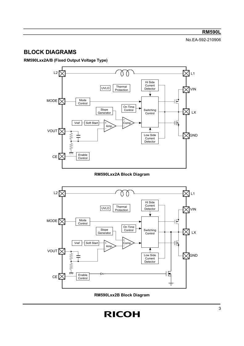
BLOCK DIAGRAMS
RM590Lxx2A/B (Fixed Output Voltage Type)
CE
VIN
LX
Enable Control
UVLO
Vref
GND
Thermal Protection
MODE
VOUT
Switching Control
Hi Side Current Detector
Low Side Current Detector
Comp. Amp.
Soft Start
Mode Control
On Time Control Slope
Generator
L1 L2
RM590Lxx2A Block Diagram
CE
VIN
LX
Enable Control
UVLO
Vref
GND
Thermal Protection
MODE
VOUT
Switching Control
Hi Side Current Detector
Low Side Current Detector
Comp. Amp.
Soft Start
Mode Control
On Time Control Slope
Generator
L1 L2
RM590Lxx2B Block Diagram
RM590L No.EA-592-210906
4
RM590L002C/D (Adjustable Output Voltage Type)
CE
VIN
LX
Enable Control
UVLO
Vref
GND
Thermal Protection
MODE
VFB
Switching Control
Hi Side Current Detector
Low Side Current Detector
Comp. Amp.
Soft Start
Mode Control
On Time Control Slope
Generator
L1 L2
RM590L002C Block Diagram
CE
VIN
LX
Enable Control
UVLO
Vref
GND
Thermal Protection
MODE
VFB
Switching Control
Hi Side Current Detector
Low Side Current Detector
Comp. Amp.
Soft Start
Mode Control
On Time Control Slope
Generator
L1 L2
RM590L002D Block Diagram
RM590L No.EA-592-210906
5
PIN DESCRIPTIONS
Top View
Bottom View
RM590L(QFN2220-8)Pin Configuration RM590L (QFN2220-8) Pin Descriptions
Pin No. Symbol I/O Description
1 VOUT/VFB I
Output/Feedback Pin Fixed Output Voltage Type: Connect to VOUT pin and L2 pin. Adjustable Output Voltage Type: Receives the feedback voltage from a Resistive divider connected across the output. Refer to “Adjustable Output Voltage Setting”
2 LX O Switch Node Connection to the Inductor. This pin connects to the drains of the internal Main and synchronous power MOSFET switches.
3 MODE I
Mode Select Input. To select forced PWM, connect this pin to a voltage above designated "High". Connecting this pin to a voltage between 0 V and designated "Low" selects PWM/VFM automatic shift operation mode.
4 L1 I Inductor Pin 1 (Input pin of inductor built-in.) Connect this pin to Lx pin.
5 VIN I Power Input Supply. Decouple this pin to GND with a capacitor.
6 CE I Forcing this pin below designated "Low" level shuts down the RM590L. In shutdown all functions are disabled except auto discharge function. (option)
7 GND I Ground Pin
8 L2 O Inductor Pin 2 (This pin connects to built-in inductor) Connect a capacitor between this pin and GND.
1 2 3
4
5 6 7
8
5 6 7
2 3
4 8
1
RM590L No.EA-592-210906
6
ABSOLUTE MAXIMUM RATINGS Symbol Item Ratings Unit
VIN Input Voltage −0.3 to 6.5 V VLX LX / L1 / L2 Pin Voltage −0.3 to VIN +0.3 V VCE CE Pin Voltage −0.3 to 6.5 V
VMODE MODE Pin Voltage −0.3 to 6.5 V VOUT/VFB VOUT / VFB Pin Voltage −0.3 to 6.5 V
ILX LX / L1 / L2 Pin Input / Output Current 1.6 A PD Power Dissipation Refer to Appendix "POWER DISSIPATION" Tj Junction Temperature Range −40 to 125 °C
Tstg Storage Temperature Range −55 to 125 °C
ABSOLUTE MAXIMUM RATINGS
Electronic and mechanical stress momentarily exceeded absolute maximum ratings may cause permanent damage and may degrade the lifetime and safety for both device and system using the device in the field. The functional operation at or over these absolute maximum ratings are not assured.
ELECTROSTATIC DISCHARGE (ESD) RATINGS
Symbol Conditions Ratings Unit VHBM HBM C = 100pF, R = 1.5kΩ -750 / +2000 V VCDM CDM ± 1000 V
ELECTROSTATIC DISCHARGE RATINGS
The electrostatic discharge test is done based on JESD47. In the HBM method, ESD is applied using the power supply pin and GND pin as reference pins.
RECOMMENDED OPERATING CONDITIONS Symbol Item Ratings Unit
VIN Input Voltage 2.3 to 5.5 V Ta Operating Temperature Range −40 to 85 °C
RECOMMENDED OPERATING CONDITIONS
All of electronic equipment should be designed that the mounted semiconductor devices operate within the recommended operating conditions. The semiconductor devices cannot operate normally over the recommended operating conditions, even if they are used over such ratings by momentary electronic noise or surge. And the semiconductor devices may receive serious damage when they continue to operate over the recommended operating conditions.
RM590L No.EA-592-210906
7
ELECTRICAL CHARACTERISTICS
The specifications surrounded by are guaranteed by design engineering at -40°C ≤ Ta ≤ 85°C.
RM590Lxx2A/B Electrical Characteristics (Ta = 25°C) Symbol Parameter Conditions Min. Typ. Max. Unit
VOUT Output Voltage
VIN = VCE = 3.6 V (VSET ≤ 2.6 V), VIN = VCE = VSET + 1 V (VSET > 2.6 V)
VSET ≥ 1.2 V x 0.985 x 1.015 V
VSET < 1.2 V −0.018 +0.018
fOSC Oscillator Frequency VIN = VCE = 3.6 V, VSET = 1.8 V, "Closed Loop Control" 4.8 6.0 7.2 MHz
IDD Supply Current VIN = VCE = VOUT = 3.6 V, VMODE = 0 V 15 µA ISTANDBY Standby Current VIN = 5.5 V, VCE = 0 V 0 5 µA
ICEH CE "High" Input Current VIN = VCE = 5.5 V −1 0 1 µA ICEL CE "Low" Input Current VIN = 5.5 V, VCE = 0 V −1 0 1 µA
IMODEH MODE "High" Input Current VIN = VMODE = 5.5 V, VCE = 0 V −1 0 1 µA IMODEL MODE "Low" Input Current VIN = 5.5 V, VCE = VMODE = 0 V −1 0 1 µA IVOUTH VOUT "High" Input Current VIN = VOUT = 5.5 V, VCE = 0 V −1 0 1 µA IVOUTL VOUT "Low" Input Current VIN = 5.5 V, VCE = VOUT = 0 V −1 0 1 µA
RDISTR Auto-discharge MOSFET On-resistance (1) VIN = 3.6 V, VCE = 0 V 40 Ω
ILXLEAKH LX "High" Leakage Current VIN = VLX = 5.5 V, VCE = 0 V −1 0 5 µA ILXLEAKL LX "Low" Leakage Current VIN = 5.5 V, VCE = VLX = 0 V −5 0 1 µA VCEH CE "High" Input Voltage VIN = 5.5 V 1.0 V VCEL CE "Low" Input Voltage VIN = 2.3 V 0.4 V
VMODEH MODE "High" Input Voltage VIN = VCE = 5.5 V 1.0 V
VMODEL MODE "Low" Input Voltage VSET ≤ 2.3 V, VIN = VCE = 2.3 V VSET > 2.3 V, VIN = VSET 0.4 V
RONP On-resistance of High Side MOSFET VIN = 3.6 V, ILX = −100 mA 0.245 Ω RONN On-resistance of Low Side MOSFET VIN = 3.6 V, ILX = −100 mA 0.225 Ω
Maxduty Maximum Duty Cycle 100 %
tSTART Soft-start Time VIN = VCE = 3.6 V (VSET ≤ 2.6 V), VIN = VCE = VSET + 1 V (VSET > 2.6 V) 150 300 µs
ILXLIM LX Current Limit VIN = VCE = 3.6 V (VSET ≤ 2.6 V), VIN = VCE = VSET + 1 V (VSET > 2.6 V) 600 1000 mA
VUVLO1 UVLO Threshold Voltage
VIN = VCE, Falling 1.85 2.00 2.20 V
VUVLO2 VIN = VCE, Rising 1.90 2.05 2.25 V
All test items listed under Electrical Characteristics are done under the pulse load condition (Tj ≈ Ta = 25°C). Test circuit is operated with “Open Loop Control” (GND = 0 V), unless otherwise specified.
(1) RM590Lxx2B only
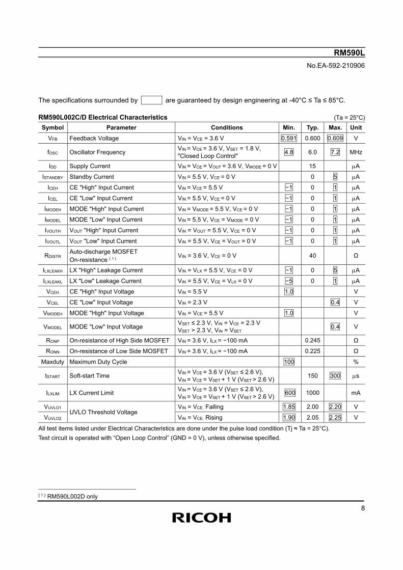
RM590L No.EA-592-210906
8
The specifications surrounded by are guaranteed by design engineering at -40°C ≤ Ta ≤ 85°C.
RM590L002C/D Electrical Characteristics (Ta = 25°C) Symbol Parameter Conditions Min. Typ. Max. Unit
VFB Feedback Voltage VIN = VCE = 3.6 V 0.591 0.600 0.609 V
fOSC Oscillator Frequency VIN = VCE = 3.6 V, VSET = 1.8 V, "Closed Loop Control" 4.8 6.0 7.2 MHz
IDD Supply Current VIN = VCE = VOUT = 3.6 V, VMODE = 0 V 15 µA
ISTANDBY Standby Current VIN = 5.5 V, VCE = 0 V 0 5 µA
ICEH CE "High" Input Current VIN = VCE = 5.5 V −1 0 1 µA
ICEL CE "Low" Input Current VIN = 5.5 V, VCE = 0 V −1 0 1 µA
IMODEH MODE "High" Input Current VIN = VMODE = 5.5 V, VCE = 0 V −1 0 1 µA
IMODEL MODE "Low" Input Current VIN = 5.5 V, VCE = VMODE = 0 V −1 0 1 µA
IVOUTH VOUT "High" Input Current VIN = VOUT = 5.5 V, VCE = 0 V −1 0 1 µA
IVOUTL VOUT "Low" Input Current VIN = 5.5 V, VCE = VOUT = 0 V −1 0 1 µA
RDISTR Auto-discharge MOSFET On-resistance (1) VIN = 3.6 V, VCE = 0 V 40 Ω
ILXLEAKH LX "High" Leakage Current VIN = VLX = 5.5 V, VCE = 0 V −1 0 5 µA
ILXLEAKL LX "Low" Leakage Current VIN = 5.5 V, VCE = VLX = 0 V −5 0 1 µA
VCEH CE "High" Input Voltage VIN = 5.5 V 1.0 V
VCEL CE "Low" Input Voltage VIN = 2.3 V 0.4 V
VMODEH MODE "High" Input Voltage VIN = VCE = 5.5 V 1.0 V
VMODEL MODE "Low" Input Voltage VSET ≤ 2.3 V, VIN = VCE = 2.3 V VSET > 2.3 V, VIN = VSET 0.4 V
RONP On-resistance of High Side MOSFET VIN = 3.6 V, ILX = −100 mA 0.245 Ω
RONN On-resistance of Low Side MOSFET VIN = 3.6 V, ILX = −100 mA 0.225 Ω
Maxduty Maximum Duty Cycle 100 %
tSTART Soft-start Time VIN = VCE = 3.6 V (VSET ≤ 2.6 V), VIN = VCE = VSET + 1 V (VSET > 2.6 V) 150 300 µs
ILXLIM LX Current Limit VIN = VCE = 3.6 V (VSET ≤ 2.6 V), VIN = VCE = VSET + 1 V (VSET > 2.6 V) 600 1000 mA
VUVLO1 UVLO Threshold Voltage
VIN = VCE, Falling 1.85 2.00 2.20 V
VUVLO2 VIN = VCE, Rising 1.90 2.05 2.25 V
All test items listed under Electrical Characteristics are done under the pulse load condition (Tj ≈ Ta = 25°C). Test circuit is operated with “Open Loop Control” (GND = 0 V), unless otherwise specified.
(1) RM590L002D only
RM590L No.EA-592-210906
9
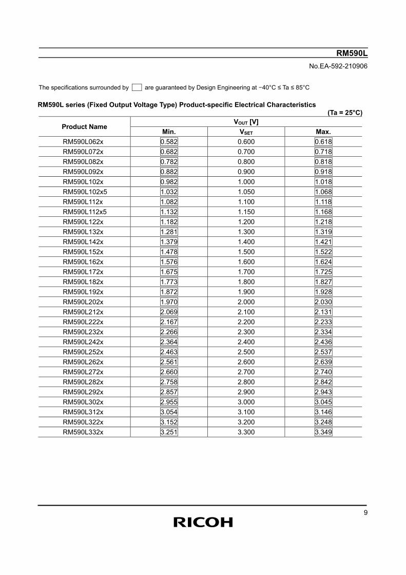
The specifications surrounded by are guaranteed by Design Engineering at −40°C ≤ Ta ≤ 85°C RM590L series (Fixed Output Voltage Type) Product-specific Electrical Characteristics
(Ta = 25°C)
Product Name VOUT [V]
Min. VSET Max. RM590L062x 0.582 0.600 0.618 RM590L072x 0.682 0.700 0.718 RM590L082x 0.782 0.800 0.818 RM590L092x 0.882 0.900 0.918 RM590L102x 0.982 1.000 1.018 RM590L102x5 1.032 1.050 1.068 RM590L112x 1.082 1.100 1.118 RM590L112x5 1.132 1.150 1.168 RM590L122x 1.182 1.200 1.218 RM590L132x 1.281 1.300 1.319 RM590L142x 1.379 1.400 1.421 RM590L152x 1.478 1.500 1.522 RM590L162x 1.576 1.600 1.624 RM590L172x 1.675 1.700 1.725 RM590L182x 1.773 1.800 1.827 RM590L192x 1.872 1.900 1.928 RM590L202x 1.970 2.000 2.030 RM590L212x 2.069 2.100 2.131 RM590L222x 2.167 2.200 2.233 RM590L232x 2.266 2.300 2.334 RM590L242x 2.364 2.400 2.436 RM590L252x 2.463 2.500 2.537 RM590L262x 2.561 2.600 2.639 RM590L272x 2.660 2.700 2.740 RM590L282x 2.758 2.800 2.842 RM590L292x 2.857 2.900 2.943 RM590L302x 2.955 3.000 3.045 RM590L312x 3.054 3.100 3.146 RM590L322x 3.152 3.200 3.248 RM590L332x 3.251 3.300 3.349
RM590L No.EA-592-210906
10
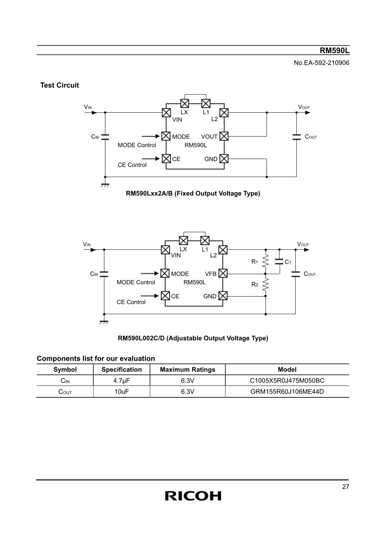
TYPIC AL APPLICATION CIRCUIT
RM590Lxx2A/B (Fixed Output Voltage Type)
RM590L002C/D (Adjustable Output Voltage Type)
Recommended External Components
Symbol Descriptions CIN 4.7 µF and more, Ceramic Capacitor
COUT 10 µF, Ceramic Capacitor
VIN
CE
L2
VOUT
GND
VIN
CIN COUT
VOUT
RM590L MODE
LX L1
MODE Control
CE Control
VIN
CE
L2
VFB
GND
VIN
CIN COUT
VOUT
RM590L MODE
LX L1
R2
C1 R1
MODE Control
CE Control

RM590L No.EA-592-210906
11
Precautions for the Selection of External Parts
Choose a low ESR ceramic capacitor. The capacitance of CIN between VIN and GND should be more than or equal to 4.7 µF. The capacitance of a ceramic capacitor (COUT) should be 10 µF. Also, choose the capacitor with consideration for bias characteristics and input/output voltages.
RM590L No.EA-592-210906
12
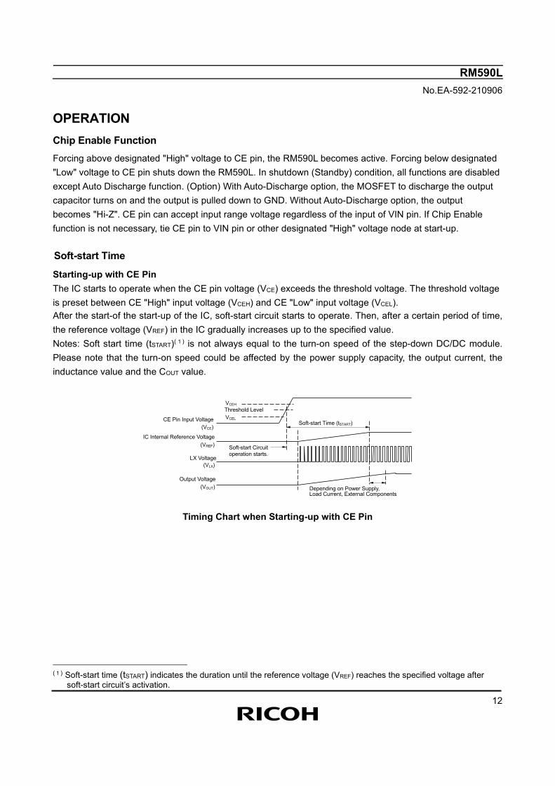
OPERATION Chip Enable Function Forcing above designated "High" voltage to CE pin, the RM590L becomes active. Forcing below designated "Low" voltage to CE pin shuts down the RM590L. In shutdown (Standby) condition, all functions are disabled except Auto Discharge function. (Option) With Auto-Discharge option, the MOSFET to discharge the output capacitor turns on and the output is pulled down to GND. Without Auto-Discharge option, the output becomes "Hi-Z". CE pin can accept input range voltage regardless of the input of VIN pin. If Chip Enable function is not necessary, tie CE pin to VIN pin or other designated "High" voltage node at start-up. Soft-start Time Starting-up with CE Pin The IC starts to operate when the CE pin voltage (VCE) exceeds the threshold voltage. The threshold voltage is preset between CE "High" input voltage (VCEH) and CE "Low" input voltage (VCEL). After the start-of the start-up of the IC, soft-start circuit starts to operate. Then, after a certain period of time, the reference voltage (VREF) in the IC gradually increases up to the specified value. Notes: Soft start time (tSTART)(1) is not always equal to the turn-on speed of the step-down DC/DC module. Please note that the turn-on speed could be affected by the power supply capacity, the output current, the inductance value and the COUT value.
VCEH
Soft-start Time (tSTART)
IC Internal Reference Voltage
VCEL Threshold Level
LX Voltage
(VCE)
(VREF) Soft-start Circuit operation starts.
(VLX)
Depending on Power Supply, Load Current, External Components
(VOUT) Output Voltage
CE Pin Input Voltage
Timing Chart when Starting-up with CE Pin
(1) Soft-start time (tSTART) indicates the duration until the reference voltage (VREF) reaches the specified voltage after
soft-start circuit’s activation.
RM590L No.EA-592-210906
13
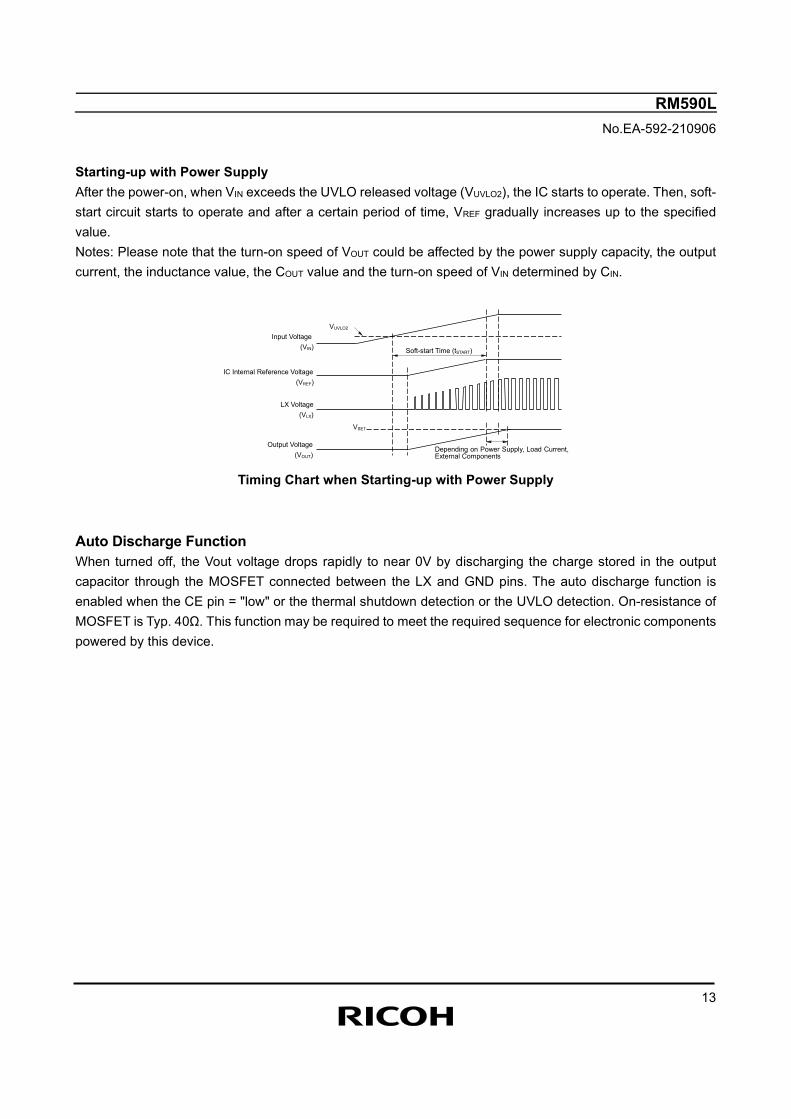
Starting-up with Power Supply After the power-on, when VIN exceeds the UVLO released voltage (VUVLO2), the IC starts to operate. Then, soft-start circuit starts to operate and after a certain period of time, VREF gradually increases up to the specified value. Notes: Please note that the turn-on speed of VOUT could be affected by the power supply capacity, the output current, the inductance value, the COUT value and the turn-on speed of VIN determined by CIN.
Output Voltage (VOUT)
Input Voltage (VIN)
VUVLO2
IC Internal Reference Voltage (VREF)
LX Voltage (VLX)
VSET
Depending on Power Supply, Load Current, External Components
Soft-start Time (tSTART)
Timing Chart when Starting-up with Power Supply
Auto Discharge Function When turned off, the Vout voltage drops rapidly to near 0V by discharging the charge stored in the output capacitor through the MOSFET connected between the LX and GND pins. The auto discharge function is enabled when the CE pin = "low" or the thermal shutdown detection or the UVLO detection. On-resistance of MOSFET is Typ. 40Ω. This function may be required to meet the required sequence for electronic components powered by this device.
RM590L No.EA-592-210906
14
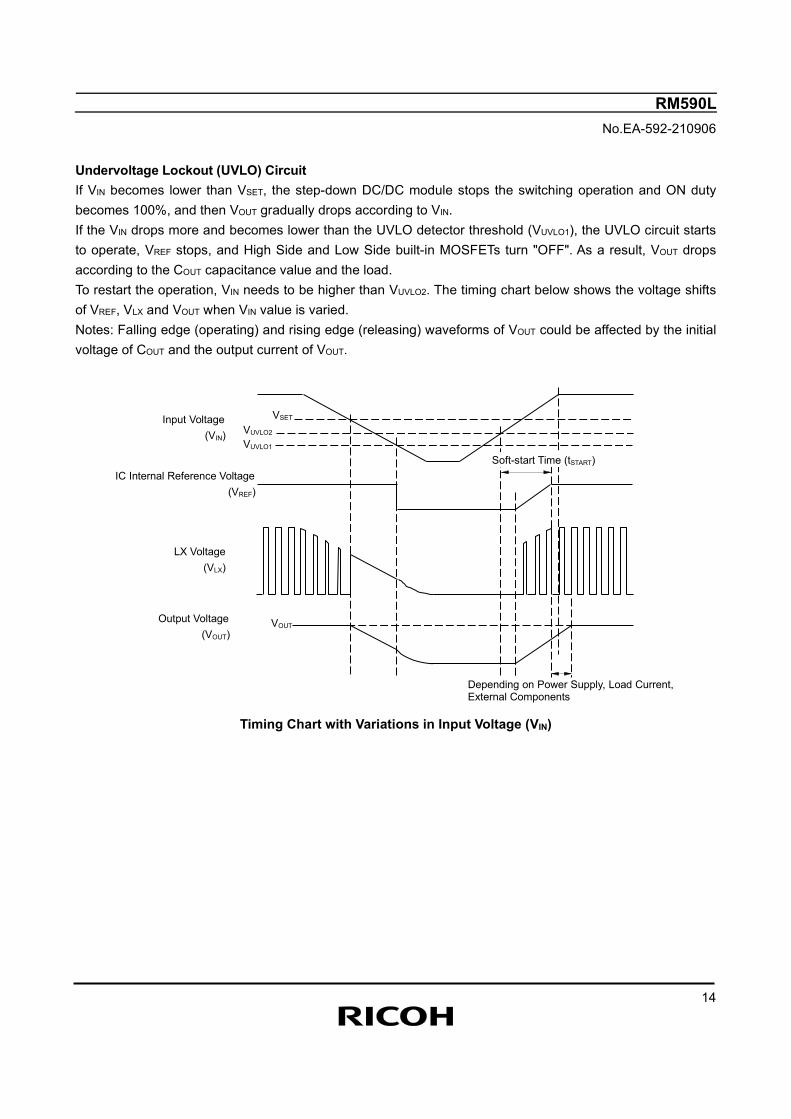
Undervoltage Lockout (UVLO) Circuit If VIN becomes lower than VSET, the step-down DC/DC module stops the switching operation and ON duty becomes 100%, and then VOUT gradually drops according to VIN. If the VIN drops more and becomes lower than the UVLO detector threshold (VUVLO1), the UVLO circuit starts to operate, VREF stops, and High Side and Low Side built-in MOSFETs turn "OFF". As a result, VOUT drops according to the COUT capacitance value and the load. To restart the operation, VIN needs to be higher than VUVLO2. The timing chart below shows the voltage shifts of VREF, VLX and VOUT when VIN value is varied. Notes: Falling edge (operating) and rising edge (releasing) waveforms of VOUT could be affected by the initial voltage of COUT and the output current of VOUT.
Output Voltage (VOUT)
Input Voltage (VIN) VUVLO2
IC Internal Reference Voltage (VREF)
VUVLO1
LX Voltage (VLX)
VSET
VOUT
Depending on Power Supply, Load Current, External Components
Soft-start Time (tSTART)
Timing Chart with Variations in Input Voltage (VIN)
RM590L No.EA-592-210906
15
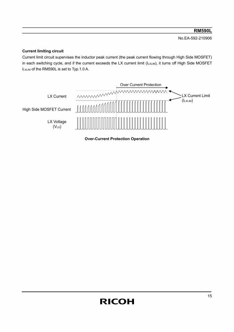
Current limiting circuit Current limit circuit supervises the inductor peak current (the peak current flowing through High Side MOSFET) in each switching cycle, and if the current exceeds the LX current limit (ILXLIM), it turns off High Side MOSFET ILXLIM of the RM590L is set to Typ.1.0 A.
LX Current Limit (ILXLIM)
LX Current
High Side MOSFET Current
LX Voltage (VLX)
Over Current Protection
Over-Current Protection Operation
RM590L No.EA-592-210906
16
Operation of Step-down DC/DC module and Output Current
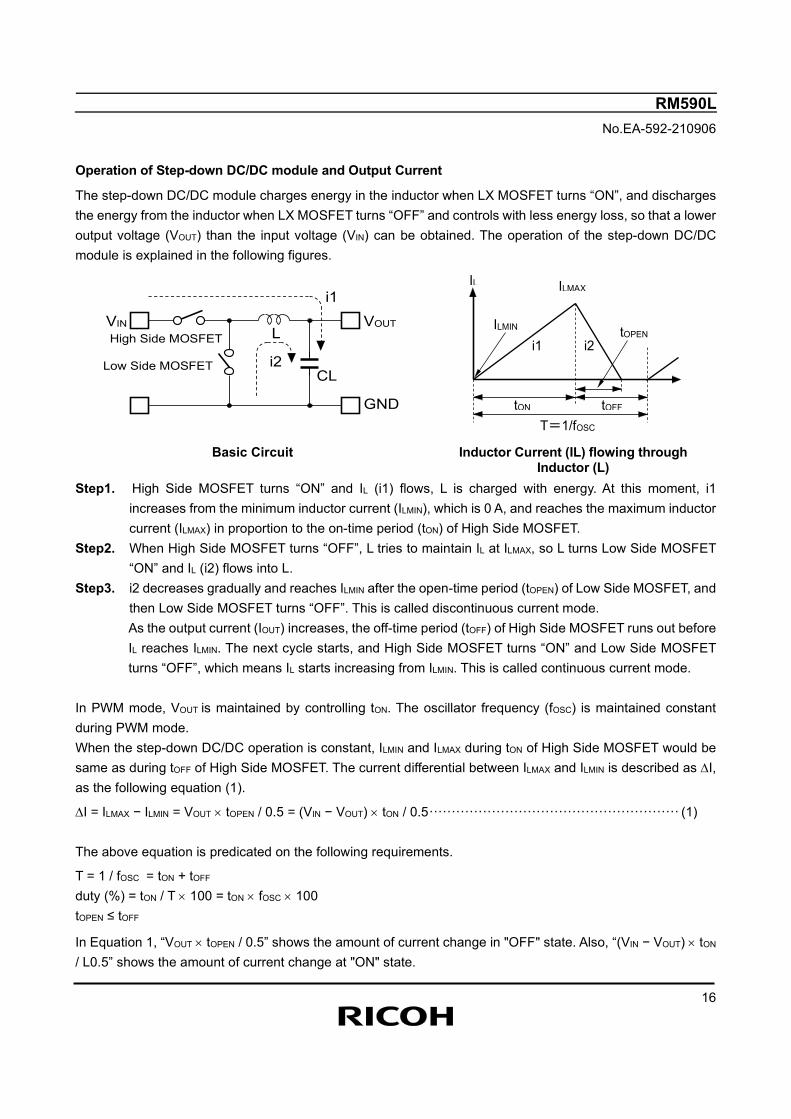
The step-down DC/DC module charges energy in the inductor when LX MOSFET turns “ON”, and discharges the energy from the inductor when LX MOSFET turns “OFF” and controls with less energy loss, so that a lower output voltage (VOUT) than the input voltage (VIN) can be obtained. The operation of the step-down DC/DC module is explained in the following figures.
High Side MOSFET L
Low Side MOSFET
VIN i1
VOUT
CL i2
GND
T=1/fOSC tON tOFF
tOPEN ILMIN
ILMAX IL
i1 i2
Basic Circuit Inductor Current (IL) flowing through
Inductor (L) Step1. High Side MOSFET turns “ON” and IL (i1) flows, L is charged with energy. At this moment, i1
increases from the minimum inductor current (ILMIN), which is 0 A, and reaches the maximum inductor current (ILMAX) in proportion to the on-time period (tON) of High Side MOSFET.
Step2. When High Side MOSFET turns “OFF”, L tries to maintain IL at ILMAX, so L turns Low Side MOSFET “ON” and IL (i2) flows into L.
Step3. i2 decreases gradually and reaches ILMIN after the open-time period (tOPEN) of Low Side MOSFET, and then Low Side MOSFET turns “OFF”. This is called discontinuous current mode. As the output current (IOUT) increases, the off-time period (tOFF) of High Side MOSFET runs out before IL reaches ILMIN. The next cycle starts, and High Side MOSFET turns “ON” and Low Side MOSFET turns “OFF”, which means IL starts increasing from ILMIN. This is called continuous current mode.
In PWM mode, VOUT is maintained by controlling tON. The oscillator frequency (fOSC) is maintained constant during PWM mode. When the step-down DC/DC operation is constant, ILMIN and ILMAX during tON of High Side MOSFET would be same as during tOFF of High Side MOSFET. The current differential between ILMAX and ILMIN is described as ∆I, as the following equation (1).
∆I = ILMAX − ILMIN = VOUT × tOPEN / 0.5 = (VIN − VOUT) × tON / 0.5 ························································ (1) The above equation is predicated on the following requirements.
T = 1 / fOSC = tON + tOFF duty (%) = tON / T × 100 = tON × fOSC × 100 tOPEN ≤ tOFF
In Equation 1, “VOUT × tOPEN / 0.5” shows the amount of current change in "OFF" state. Also, “(VIN − VOUT) × tON / L0.5” shows the amount of current change at "ON" state.
RM590L No.EA-592-210906
17
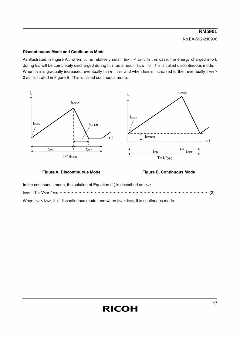
Discontinuous Mode and Continuous Mode As illustrated in Figure A., when IOUT is relatively small, tOPEN < tOFF. In this case, the energy charged into L during tON will be completely discharged during tOFF, as a result, ILMIN = 0. This is called discontinuous mode. When IOUT is gradually increased, eventually tOPEN = tOFF and when IOUT is increased further, eventually ILMIN > 0 as illustrated in Figure B. This is called continuous mode.
ILMAX
ILMIN
tON tOFF
T=1/fOSC
tOPEN
IL
t
ILMAX
ILMIN
tON tOFF T=1/fOSC
IL
ICONST t
Figure A. Discontinuous Mode Figure B. Continuous Mode
In the continuous mode, the solution of Equation (1) is described as tONC.
tONC = T × VOUT / VIN ··············································································································· (2)
When tON < tONC, it is discontinuous mode, and when tON = tONC, it is continuous mode.
RM590L No.EA-592-210906
18
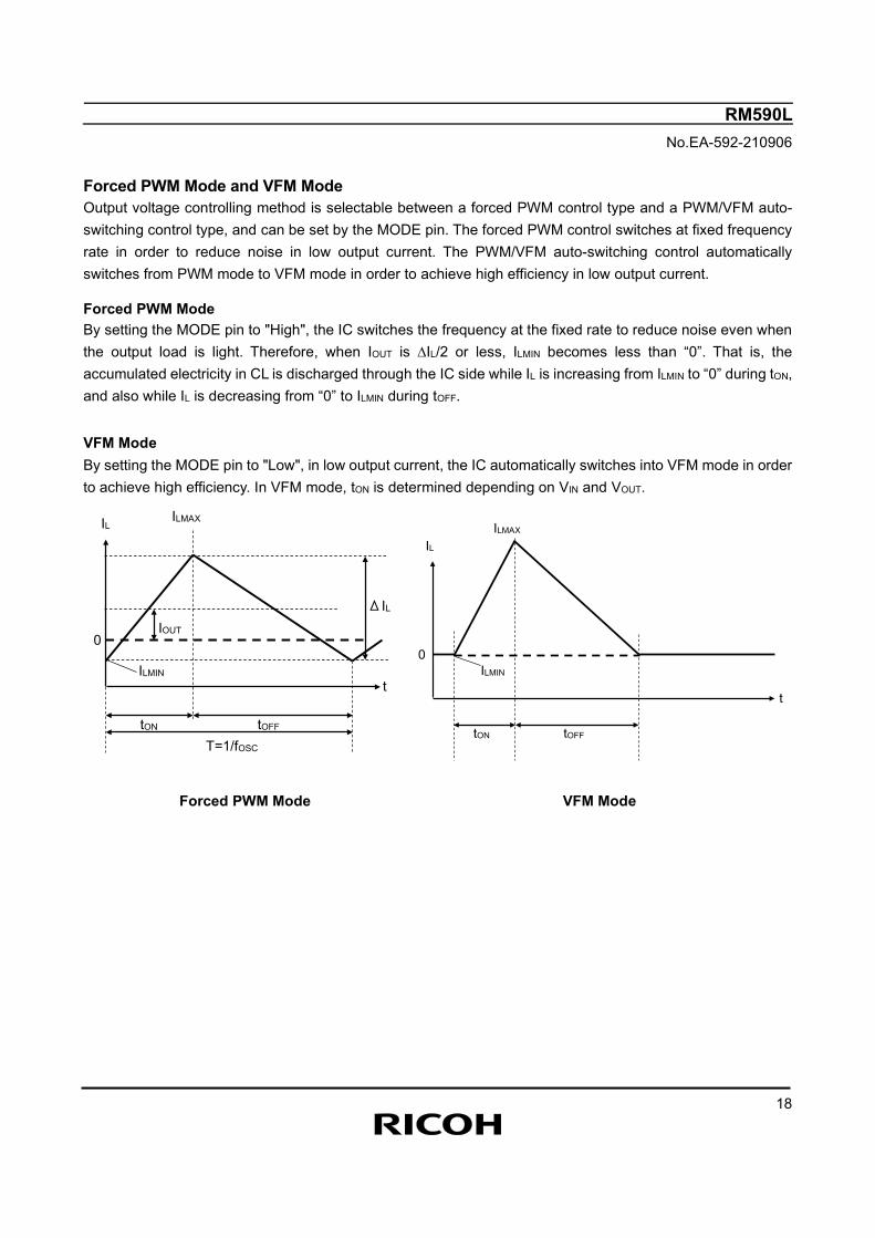
Forced PWM Mode and VFM Mode Output voltage controlling method is selectable between a forced PWM control type and a PWM/VFM auto-switching control type, and can be set by the MODE pin. The forced PWM control switches at fixed frequency rate in order to reduce noise in low output current. The PWM/VFM auto-switching control automatically switches from PWM mode to VFM mode in order to achieve high efficiency in low output current. Forced PWM Mode By setting the MODE pin to "High", the IC switches the frequency at the fixed rate to reduce noise even when the output load is light. Therefore, when IOUT is ∆IL/2 or less, ILMIN becomes less than “0”. That is, the accumulated electricity in CL is discharged through the IC side while IL is increasing from ILMIN to “0” during tON, and also while IL is decreasing from “0” to ILMIN during tOFF.
VFM Mode By setting the MODE pin to "Low", in low output current, the IC automatically switches into VFM mode in order to achieve high efficiency. In VFM mode, tON is determined depending on VIN and VOUT.
ILMAX
ILMIN
tON tOFF T=1/fOSC
IL
IOUT
t
0
ΔIL
ILMAX
ILMIN
tON tOFF
IL
t
0
Forced PWM Mode VFM Mode
RM590L No.EA-592-210906
19
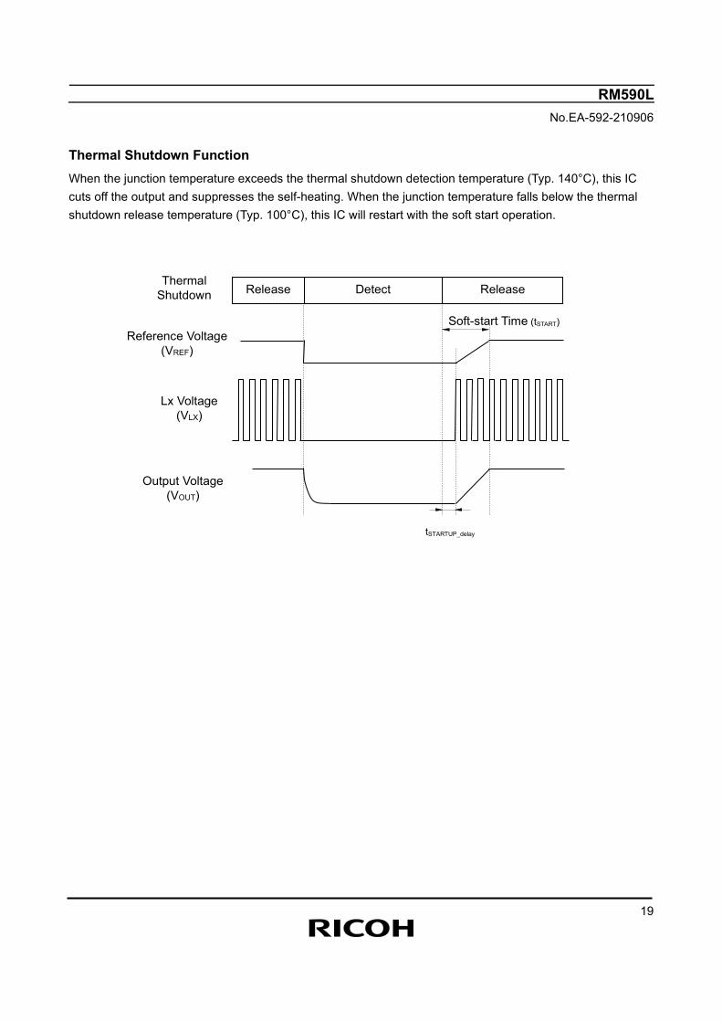
Thermal Shutdown Function When the junction temperature exceeds the thermal shutdown detection temperature (Typ. 140°C), this IC cuts off the output and suppresses the self-heating. When the junction temperature falls below the thermal shutdown release temperature (Typ. 100°C), this IC will restart with the soft start operation.
Output Voltage (VOUT)
Thermal Shutdown
Reference Voltage (VREF)
Lx Voltage (VLX)
Soft-start Time (tSTART)
Release Detect Release
tSTARTUP_delay
RM590L No.EA-592-210906
20
2.3
3.1
3.9
4.7
5.5
0.6 1.2 1.8 2.4 3.0 3.6 4.2
Inpu
t Vol
tage
VIN
(V)
Output Voltage VOUT (V)
TECHNICAL NOTES The performance of a power source circuit using this device is highly dependent on a peripheral circuit. A peripheral component or the device mounted on PCB should not exceed its rated voltage, rated current or rated power. When designing a peripheral circuit, please be fully aware of the following points. • Set the external components as close as possible to the IC and minimize the wiring between the
components and the IC. Especially, place a capacitor (CIN) as close as possible to the VIN pin and GND.
• Ensure the VIN and GND lines are sufficiently robust. If their impedance is too high, noise pickup or unstable operation may result.
• A large switching current flows through the VIN line, GND line, VOUT line, inductor, LX, L1 and L2. Make the wirings short and wide.
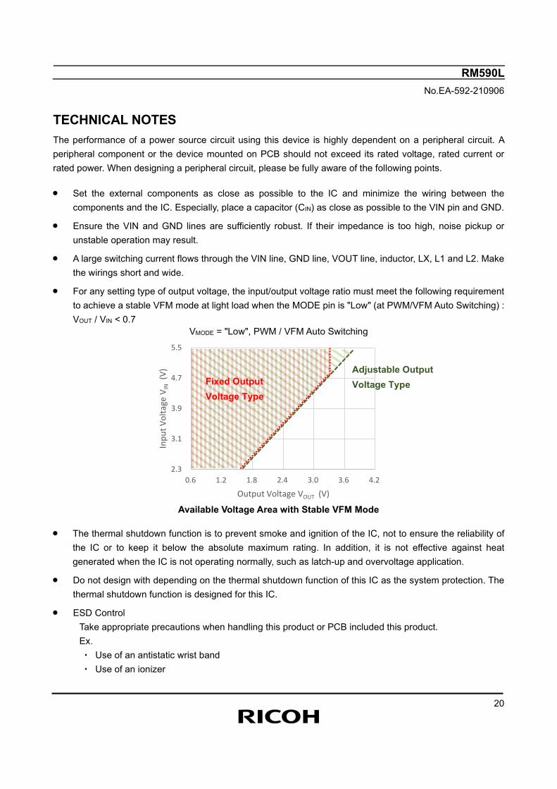
• For any setting type of output voltage, the input/output voltage ratio must meet the following requirement to achieve a stable VFM mode at light load when the MODE pin is "Low" (at PWM/VFM Auto Switching) : VOUT / VIN < 0.7
VMODE = "Low", PWM / VFM Auto Switching
Available Voltage Area with Stable VFM Mode
• The thermal shutdown function is to prevent smoke and ignition of the IC, not to ensure the reliability of the IC or to keep it below the absolute maximum rating. In addition, it is not effective against heat generated when the IC is not operating normally, such as latch-up and overvoltage application.
• Do not design with depending on the thermal shutdown function of this IC as the system protection. The thermal shutdown function is designed for this IC.
• ESD Control Take appropriate precautions when handling this product or PCB included this product. Ex.
・ Use of an antistatic wrist band ・ Use of an ionizer
Adjustable Output Voltage Type Fixed Output
Voltage Type
RM590L No.EA-592-210906
21
APPLICATION INFORMATION Adjustable Output Voltage Setting (RM590L002C/D) By connecting divider resistors (R1, R2) to the VFB pin, the set output voltage (VSET) can be set using the following equation.
VSET = VFB × (R1 + R2) / R2
The reference voltage (VFB) of this IC is set to 0.6 V, and the accuracy of VFB and the output voltage setting range are as follows.
VSET: 0.6V ≤ VSET ≤ 5.5 V VFB : 0.6 V ± 9mV
Refer to the following table for the recommended values for R1, R2 and C1. Set Output Voltage (VSET) vs. R1 / R2 / C1 (Adjustable Output Voltage Type)
VSET [V] R1 [kΩ] R2 [kΩ] C1 [pF] 0.6 0 220 Open
0.6 < VSET ≤ 0.9
R1 = (VSET / VFB -1) x R2
220 47 0.9 < VSET ≤ 1.8 220 33 1.8 < VSET ≤ 2.1 150 10 2.1 < VSET ≤ 2.4 100 10 2.4 < VSET ≤ 2.7 68 10 2.7 < VSET ≤ 3.0 47 10 3.0 < VSET ≤ VIN 47 6.8
RM590L No.EA-592-210906
22
PCB Layout RM590L (QFN2220-8) Board Diagram
Top Layer Bottom Layer
RM590L No.EA-592-210906
23
TYPICAL CHARACTERISTICS Note: Typical Characteristics are intended to be used as reference data; they are not guaranteed. 1) Efficiency vs. Output Current VOUT=0.9V VOUT=1.2V
VOUT=1.8V VOUT=3.3V
2) Output Voltage vs. Output Current VIN=3.6V, VOUT=1.8V VIN=3.6V, VOUT=1.8V MODE = "H" Forced PWM Mode MODE = "L" PWM/VFM Auto Switching
0102030405060708090
100
0.01 0.1 1 10 100 1000
Effic
ienc
y η
[%]
Output Current IOUT [mA]
"2.7V""3.6V""4.2V""5.0V"
VFM / PWM Auto
VIN = 2.7V VIN = 3.6VVIN = 4.2VVIN = 5.0V
Forced PWMVIN = 3.6V
0102030405060708090
100
0.01 0.1 1 10 100 1000Ef
ficie
ncy
η [%
]
Output Current IOUT [mA]
VIN = 2.7VVIN = 3.6VVIN = 4.2VVIN = 5.0V
VFM / PWM Auto
Forced PWMVIN = 3.6V
VIN = 2.7V VIN = 3.6VVIN = 4.2VVIN = 5.0V
0102030405060708090
100
0.01 0.1 1 10 100 1000
Effic
ienc
y η
[%]
Output Current IOUT [mA]
VIN = 2.7VVIN = 3.6VVIN = 4.2VVIN = 5.0V
VIN = 2.7V VIN = 3.6VVIN = 4.2VVIN = 5.0V
VFM / PWM Auto
Forced PWMVIN = 3.6V
0102030405060708090
100
0.01 0.1 1 10 100 1000
Effic
ienc
y η
[%]
Output Current IOUT [mA]
VIN = 4.2VVIN = 5.0V
VFM / PWM Auto
VIN = 4.2VVIN = 5.0V
Forced PWMVIN = 4.2V
1.77
1.78
1.79
1.80
1.81
1.82
1.83
0 100 200 300 400
Out
put V
olta
ge V
OU
T[V
]
Output Current IOUT [mA]
1.77
1.78
1.79
1.80
1.81
1.82
1.83
0 100 200 300 400
Out
put V
olta
ge V
OU
T [V
]
Output Current IOUT [mA]
RM590L No.EA-592-210906
24
3) Oscillator Frequency vs. Input Voltage IOUT=1mA IOUT=1mA MODE = "H" Forced PWM Mode MODE = "L" PWM/VFM Auto Switching
IOUT=200mA IOUT=200mA MODE = "H" Forced PWM Mode MODE = "L" PWM/VFM Auto Switching
4) Ripple Voltage vs. Input Voltage VIN=3.6V, VOUT=1.8V VIN=3.6V, VOUT=1.8V MODE = "H" Forced PWM Mode MODE = "L" PWM/VFM Auto Switching
0
1
2
3
4
5
6
7
2.0 2.5 3.0 3.5 4.0 4.5 5.0 5.5
Freq
uenc
y fo
sc [M
Hz]
Input Voltage VIN [V]
VOUT = 0.9VVOUT = 1.2VVOUT = 1.8VVOUT = 3.3V
VOUT = 0.9VVOUT = 1.2VVOUT = 1.8VVOUT = 3.3V
020406080
100120140160180200
2.0 2.5 3.0 3.5 4.0 4.5 5.0 5.5Fr
eque
ncy
fosc
[kH
z]Input Voltage VIN [V]
VOUT = 0.9V
VOUT = 1.2V
VOUT = 1.8V
VOUT = 3.3V
VOUT = 0.9VVOUT = 1.2VVOUT = 1.8VVOUT = 3.3V
0
1
2
3
4
5
6
7
2.0 2.5 3.0 3.5 4.0 4.5 5.0 5.5
Freq
uenc
y fo
sc [M
Hz]
Input Voltage VIN [V]
VOUT = 0.9VVOUT = 1.2VVOUT = 1.8VVOUT = 3.3V
VOUT = 0.9VVOUT = 1.2VVOUT = 1.8VVOUT = 3.3V
0
1
2
3
4
5
6
7
2.0 2.5 3.0 3.5 4.0 4.5 5.0 5.5
Freq
uenc
y fo
sc [M
Hz]
Input Voltage VIN [V]
VOUT = 0.9VVOUT = 1.2VVOUT = 1.8VVOUT = 3.3V
VOUT = 0.9VVOUT = 1.2VVOUT = 1.8VVOUT = 3.3V
05
101520253035404550
2 3 4 5 6
Out
put V
olta
ge V
rippl
e [m
V]
Input Voltage VIN [V]
Iout = 1mAIout = 400mAIOUT = 1mAIOUT = 400mA
05
101520253035404550
2 3 4 5 6
Out
put V
olta
ge V
rippl
e [m
V]
Input Voltage VIN [V]
Iout = 1mAIout = 400mAIOUT = 1mAIOUT = 400mA
RM590L No.EA-592-210906
25
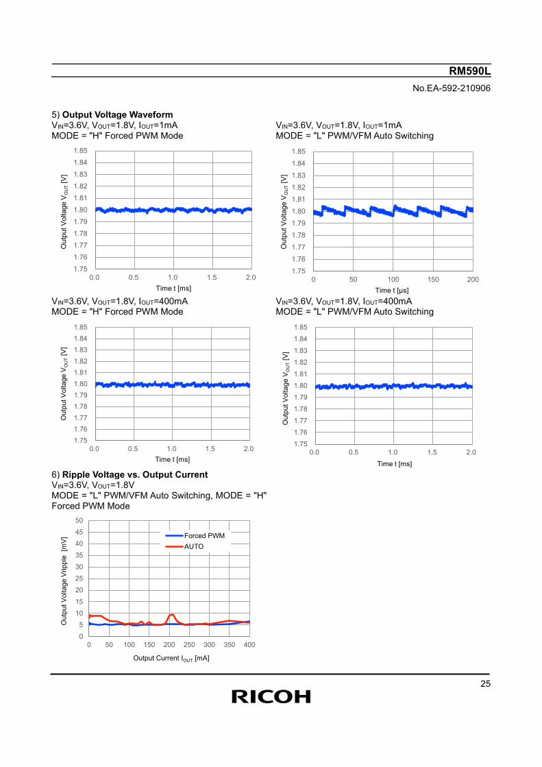
5) Output Voltage Waveform VIN=3.6V, VOUT=1.8V, IOUT=1mA VIN=3.6V, VOUT=1.8V, IOUT=1mA MODE = "H" Forced PWM Mode MODE = "L" PWM/VFM Auto Switching
VIN=3.6V, VOUT=1.8V, IOUT=400mA VIN=3.6V, VOUT=1.8V, IOUT=400mA MODE = "H" Forced PWM Mode MODE = "L" PWM/VFM Auto Switching
6) Ripple Voltage vs. Output Current VIN=3.6V, VOUT=1.8V MODE = "L" PWM/VFM Auto Switching, MODE = "H" Forced PWM Mode
1.751.761.771.781.791.801.811.821.831.841.85
0.0 0.5 1.0 1.5 2.0
Out
put V
olta
ge V
OU
T[V
]
Time t [ms]
1.751.761.771.781.791.801.811.821.831.841.85
0 50 100 150 200O
utpu
t Vol
tage
VO
UT
[V]
Time t [μs]
1.751.761.771.781.791.801.811.821.831.841.85
0.0 0.5 1.0 1.5 2.0
Out
put V
olta
ge V
OU
T[V
]
Time t [ms]
1.751.761.771.781.791.801.811.821.831.841.85
0.0 0.5 1.0 1.5 2.0
Out
put V
olta
ge V
OU
T[V
]
Time t [ms]
05
101520253035404550
0 50 100 150 200 250 300 350 400
Out
put V
olta
ge V
rippl
e [m
V]
Output Current IOUT [mA]
Forced PWMAUTO
RM590L No.EA-592-210906
26
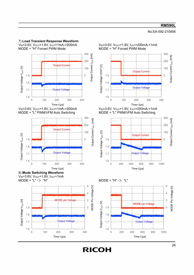
7) Load Transient Response Waveform VIN=3.6V, VOUT=1.8V, IOUT=1mA->200mA VIN=3.6V, VOUT=1.8V, IOUT=200mA->1mA MODE = "H" Forced PWM Mode MODE = "H" Forced PWM Mode
VIN=3.6V, VOUT=1.8V, IOUT=1mA->200mA VIN=3.6V, VOUT=1.8V, IOUT=200mA->1mA MODE = "L" PWM/VFM Auto Switching MODE = "L" PWM/VFM Auto Switching
8) Mode Switching Waveform VIN=3.6V, VOUT=1.8V, IOUT=1mA MODE = "L" -> "H" MODE = "H" -> "L"
0
100
200
300
1.6
1.7
1.8
1.9
0 100 200 300 400
Out
put C
urre
nt I O
UT
[mA]
Out
put V
olta
ge V
OU
T[V
]
Time t [μs]
Output Current
Output Voltage
0
100
200
300
1.6
1.7
1.8
1.9
0 100 200 300 400
Out
put C
urre
nt I O
UT
[mA]
Out
put V
olta
ge V
OU
T [V
]Time t [μs]
Output Current
Output Voltage
0
100
200
300
1.6
1.7
1.8
1.9
0 100 200 300 400
Out
put C
urre
nt I O
UT
[mA]
Out
put V
olta
ge V
OU
T[V
]
Time t [μs]
Output Current
Output Voltage
0
100
200
300
1.6
1.7
1.8
1.9
0 200 400 600 800 1000
Out
put C
urre
nt I O
UT
[mA]
Out
put V
olta
ge V
OU
T[V
]
Time t [μs]
Output Current
Output Voltage
0
2
4
6
1.6
1.7
1.8
1.9
0 100 200 300 400
MO
DE
Pin
Volta
ge [V
]
Out
put V
olta
ge V
OU
T [V
]
Time t [μs]
Output Voltage
MODE pin Voltage
0
2
4
6
1.6
1.7
1.8
1.9
0 200 400 600 800 1000
MO
DE
Pin
Volta
ge [V
]
Out
put V
olta
ge V
OU
T[V
]
Time t [μs]
Output Voltage
MODE pin Voltage
RM590L No.EA-592-210906
27
Test Circuit
RM590Lxx2A/B (Fixed Output Voltage Type)
RM590L002C/D (Adjustable Output Voltage Type)
Components list for our evaluation Symbol Specification Maximum Ratings Model
CIN 4.7µF 6.3V C1005X5R0J475M050BC
COUT 10uF 6.3V GRM155R60J106ME44D
VIN
CE
L2
VFB
GND
VIN
CIN COUT
VOUT
RM590L MODE
LX L1
R2
C1 R1
MODE Control
CE Control
VIN
CE
L2
VOUT
GND
VIN
CIN COUT
VOUT
RM590L MODE
LX L1
MODE Control
CE Control
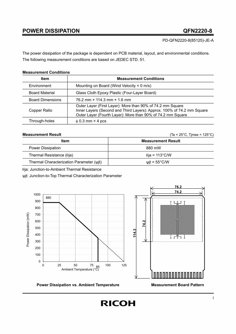
POWER DISSIPATION QFN2220-8 PD-QFN2220-8(85125)-JE-A
i
The power dissipation of the package is dependent on PCB material, layout, and environmental conditions. The following measurement conditions are based on JEDEC STD. 51. Measurement Conditions
Item Measurement Conditions Environment Mounting on Board (Wind Velocity = 0 m/s)
Board Material Glass Cloth Epoxy Plastic (Four-Layer Board)
Board Dimensions 76.2 mm × 114.3 mm × 1.6 mm
Copper Ratio Outer Layer (First Layer): More than 90% of 74.2 mm Square Inner Layers (Second and Third Layers): Approx. 100% of 74.2 mm Square Outer Layer (Fourth Layer): More than 90% of 74.2 mm Square
Through-holes φ 0.3 mm × 4 pcs
Measurement Result (Ta = 25°C, Tjmax = 125°C)
Item Measurement Result Power Dissipation 880 mW
Thermal Resistance (θja) θja = 113°C/W
Thermal Characterization Parameter (ψjt) ψjt = 55°C/W
θja: Junction-to-Ambient Thermal Resistance ψjt: Junction-to-Top Thermal Characterization Parameter
Power Dissipation vs. Ambient Temperature Measurement Board Pattern
0
100
200
300
400
500
600
700
800
900
1000
0 25 50 75 100 125
Pow
er D
issi
patio
n (m
W)
Ambient Temperature (°C)85
880
74.2
74.2 76.2
114.
3
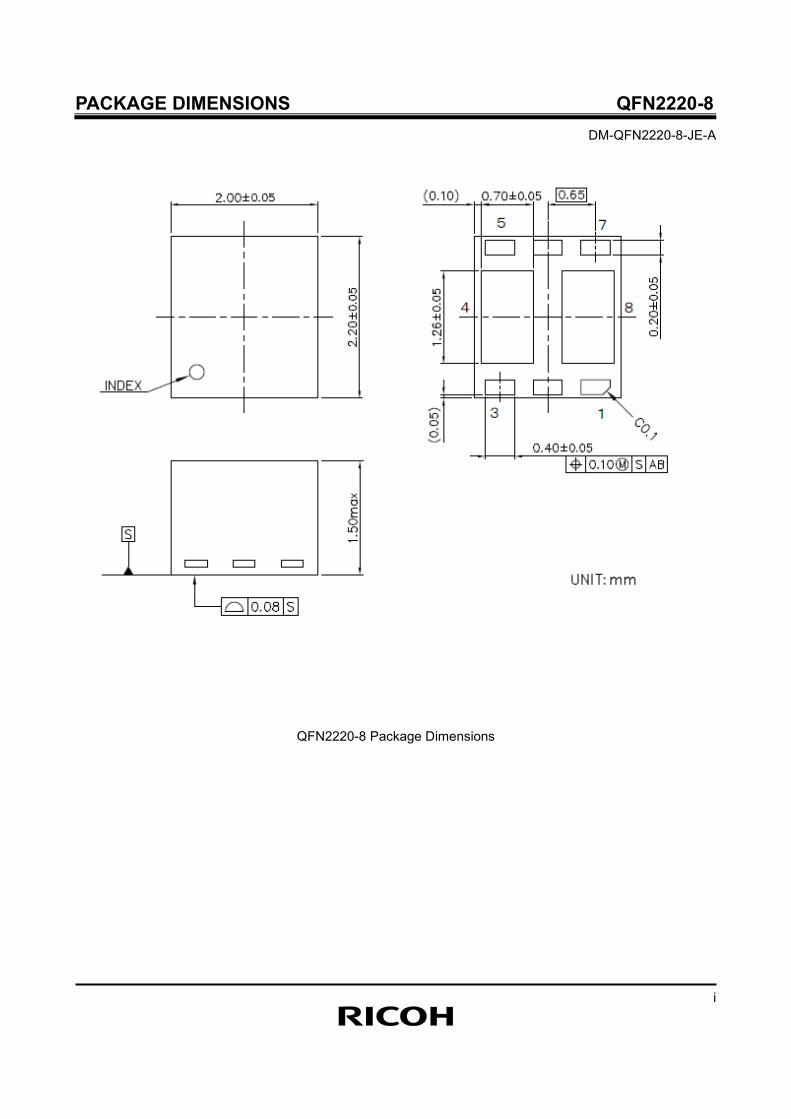
PACKAGE DIMENSIONS QFN2220-8 DM-QFN2220-8-JE-A
i
QFN2220-8 Package Dimensions *
Ricoh is committed to reducing the environmental loading materials in electrical deviceswith a view to contributing to the protection of human health and the environment. Ricoh has been providing RoHS compliant products since April 1, 2006 and Halogen-free products since April 1, 2012.Halogen Free
1. The products and the product specifications described in this document are subject to change or discontinuation ofproduction without notice for reasons such as improvement. Therefore, before deciding to use the products, pleaserefer to Ricoh sales representatives for the latest information thereon.
2. The materials in this document may not be copied or otherwise reproduced in whole or in part without prior writtenconsent of Ricoh.
3. Please be sure to take any necessary formalities under relevant laws or regulations before exporting or otherwisetaking out of your country the products or the technical information described herein.
4. The technical information described in this document shows typical characteristics of and example application circuitsfor the products. The release of such information is not to be construed as a warranty of or a grant of license underRicoh's or any third party's intellectual property rights or any other rights.
5. The products listed in this document are intended and designed for use as general electronic components in standardapplications (office equipment, telecommunication equipment, measuring instruments, consumer electronic products,amusement equipment etc.). Those customers intending to use a product in an application requiring extreme qualityand reliability, for example, in a highly specific application where the failure or misoperation of the product could resultin human injury or death (aircraft, spacevehicle, nuclear reactor control system, traffic control system, automotive andtransportation equipment, combustion equipment, safety devices, life support system etc.) should first contact us.
6. We are making our continuous effort to improve the quality and reliability of our products, but semiconductor productsare likely to fail with certain probability. In order to prevent any injury to persons or damages to property resulting fromsuch failure, customers should be careful enough to incorporate safety measures in their design, such as redundancyfeature, fire containment feature and fail-safe feature. We do not assume any liability or responsibility for any loss ordamage arising from misuse or inappropriate use of the products.
7. Anti-radiation design is not implemented in the products described in this document.8. The X-ray exposure can influence functions and characteristics of the products. Confirm the product functions andcharacteristics in the evaluation stage.
9. WLCSP products should be used in light shielded environments. The light exposure can influence functions andcharacteristics of the products under operation or storage.
10. There can be variation in the marking when different AOI (Automated Optical Inspection) equipment is used. In thecase of recognizing the marking characteristic with AOI, please contact Ricoh sales or our distributor before attemptingto use AOI.
11. Please contact Ricoh sales representatives should you have any questions or comments concerning the products orthe technical information.
Official website
https://www.n-redc.co.jp/en/Contact us
https://www.n-redc.co.jp/en/buy/