SingleN−ChannelPowerMOSFET · PJM60H07NTF SingleN−ChannelPowerMOSFET 2/6 Revision Ö1.0Nov-2017...
6
PJM60H07NTF Single N−Channel Power MOSFET www.pingjingsemi.com 1/6 Revision:1.0 Nov-2017 Features DC−fast switching ESD improved capability Low on resistance Low gate charge Low reverse transfer capacitances 100% single pulse avalanche energy test VDSS=600V ID=7A PD=40W RDSON(TYP)=0.9Ω Applications Power switch circuit of adaptor and charger TO-220F Absolute Maximum Ratings (TC=25℃unless otherwise stated) Symbol Parameter Rating Units V DSS Drain-to-Source Voltage 600 V I D Continuous Drain Current 7 A Continuous Drain Current TC=100°C 4.5 A IDM a1 Pulsed Drain Current 28 A VGS Gate-to-Source Voltage ±30 V EAS a2 Single Pulse Avalanche Energy 560 mJ EAr a1 Avalanche Energy ,Repetitive 54 mJ IAR a1 Avalanche Current 3.3 A dv/dt a3 Peak Diode Recovery dv/dt 5.0 V/ns PD Power Dissipation 40 W Derating Factor above 25°C 0.32 W/℃ V ESD(GS) Gate source ESD (HBM-C= 100pF, R=1.5kΩ) 3000 V TJ, Tstg Operating Junction and Storage Temperature Range 150 ,–55 to 150 ℃ TL Maximum Temperature for Soldering 300 ℃ a1:Repetitive rating; pulse width limited by maximum junction temperature a2:L=10mH, ID=11A, Start TJ =25 ℃ a3:I SD=7A,di/dt≤100A/us,VDD≤BV DS , Start TJ=25 ℃ 2 1 3 Gate Source Drain
Transcript of SingleN−ChannelPowerMOSFET · PJM60H07NTF SingleN−ChannelPowerMOSFET 2/6 Revision Ö1.0Nov-2017...

PJM60H07NTFSingle N−Channel Power MOSFET
www.pingjingsemi.com 1 / 6Revision:1.0 Nov-2017
Features DC−fast switching
ESD improved capability
Low on resistance
Low gate charge
Low reverse transfer capacitances
100% single pulse avalanche energy test
VDSS=600V
ID=7A
PD=40W
RDSON(TYP)=0.9Ω
Applications
Power switch circuit of adaptor and charger
TO-220F
Absolute Maximum Ratings (TC=25unless otherwise stated)Symbol Parameter Rating Units
VDSS Drain-to-Source Voltage 600 V
IDContinuous Drain Current 7 A
Continuous Drain Current TC=100°C 4.5 A
IDMa1 Pulsed Drain Current 28 A
VGS Gate-to-Source Voltage ±30 V
EASa2 Single Pulse Avalanche Energy 560 mJ
EAra1 Avalanche Energy ,Repetitive 54 mJ
IARa1 Avalanche Current 3.3 A
dv/dta3 Peak Diode Recovery dv/dt 5.0 V/ns
PD
Power Dissipation 40 W
Derating Factor above 25°C 0.32 W/
VESD(GS) Gate source ESD (HBM-C= 100pF, R=1.5kΩ) 3000 V
TJ,Tstg Operating Junction and Storage Temperature Range 150,–55 to 150
TL Maximum Temperature for Soldering 300
a1:Repetitive rating; pulse width limited by maximum junction temperaturea2:L=10mH, ID=11A, Start TJ=25a3:ISD=7A,di/dt≤100A/ us,VDD≤BVDS , Start TJ=25
2
1
3
Gate
Source
Drain

PJM60H07NTFSingle N−Channel Power MOSFET
www.pingjingsemi.com 2 / 6Revision:1.0 Nov-2017
Thermal Characteristics
Symbol Parameter Rating Units
RθJC Thermal Resistance,Junction-to-Case 3.13 / W
RθJA Thermal Resistance, Junction-to-Ambient 100 / W
Electrical Characteristics (TC=25 unless otherwise specified)
Symbol Parameter Test ConditionsRating
UnitsMin. Typ. Max.
Off CharacteristicsVDSS Drain to Source Breakdown Voltage VGS=0V,ID=250µA 600 -- -- V
ΔBVDSS/ΔTJ Bvdss Temperature Coefficient ID=250uA,Reference25 -- 0.61 -- V/
IDSS Drain to Source Leakage CurrentVDS=600V, VGS=0V,Ta=25 -- -- 10
µAVDS=480V, VGS=0V,Ta=125 -- -- 100
IGSS( F) Gate to Source Forward Leakage VGS=+20V -- -- 10 µA
IGSS( R) Gate to Source Reverse Leakage VGS=-20V -- -- -10 µA
On CharacteristicsRDS(ON) Drain-to-Source On-Resistance VGS=10V,ID=3.5A -- 0.9 1.2 Ω
VGS(TH) Gate Threshold Voltage VDS=VGS,ID=250µA 2.0 -- 4.0 V
gfs Forward Trans conductance VDS=15V,ID=3.5A -- 5 -- S
Pulse width<380μs;duty cycle<2%.
Dynamic CharacteristicsCiss Input Capacitance
VGS=0V,VDS=25V,f=1.0MHz
-- 950 --pFCoss Output Capacitance -- 98 --
Crss Reverse Transfer Capacitance -- 10 --
Resistive Switching Characteristicstd(ON) Turn-on Delay Time
ID=7A,VDD=325V
VGS=10V,Rg=9.1Ω
-- 11 --
nstr Rise Time -- 10 --
td(OFF) Turn-Off Delay Time -- 36 --
tf Fall Time -- 18 --
Qg Total Gate Charge
ID=7A,VDD=325V VGS=10V
-- 25 --nCQgs Gate to Source Charge -- 4 --
Qgd Gate to Drain (“ Miller ”)Charge -- 10 --
Source-Drain Diode CharacteristicsISD Continuous Source Current (Body Diode) -- -- 7 A
ISM Maximum Pulsed Current (Body Diode) -- -- 28 A
VSD Diode Forward Voltage IS=7A,VGS=0V -- -- 1.5 V
trr Reverse Recovery Time IS=7A,TJ=25
dIF/dt=100A/μs,VGS=0V
-- 201 -- ns
Qrr Reverse Recovery Charge -- 989 -- nC
Pulse width<380μs;duty cycle<2%.

PJM60H07NTFSingle N−Channel Power MOSFET
www.pingjingsemi.com 3 / 6Revision:1.0 Nov-2017
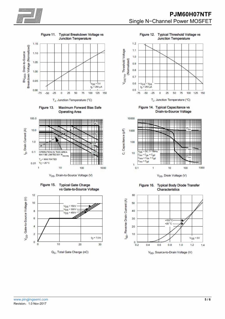
Typical Characteristic Curves

PJM60H07NTFSingle N−Channel Power MOSFET
www.pingjingsemi.com 4 / 6Revision:1.0 Nov-2017
PJM60H07NTFSingle N−Channel Power MOSFET
www.pingjingsemi.com 5 / 6Revision:1.0 Nov-2017

PJM60H07NTFSingle N−Channel Power MOSFET
www.pingjingsemi.com 6 / 6Revision:1.0 Nov-2017
Package OutlineTO-220F
Ordering informationDevice Package Shipping
PJM60H07NTF TO-220F
A A2
C
C1
D1
D2
D D
A3
H1
C2
B2
E3 E4
B1
B3
E
:
SYMBOL min nom max SYMBOL min nom maxA 9.80 10.60 D 2.54A1 7.00 D1 1.15 1.55A2 2.90 3.40 D2 0.60 1.00A3 9.10 9.90 D3 0.20 0.50
B1 15.40 16.40 E 2.24 2.84
B2 4.35 4.95 E1 0.70B3 6.00 7.40 E2 1.0×45°
C 3.00 3.70 E3 0.35 0.65C1 15.00 17.00 E4 2.30 3.30
C2 8.80 10.80 α(度) 30°
50 PCS/TUBE


![Gamma Radiation-Induced Disruption of Cellular Junctions ...downloads.hindawi.com/journals/omcl/2019/1486232.pdf · junction protein [13]. Connexins compose the gap junction channels](https://static.fdocument.org/doc/165x107/5f06b4cd7e708231d4195458/gamma-radiation-induced-disruption-of-cellular-junctions-junction-protein-13.jpg)