Single Transistor Amplifier Stages - MIT … Two Results - Exams will be ... Review - Biasing and...
25
6.012 - Microelectronic Devices and Circuits Lecture 18 - Single Transistor Amplifier Stages - Outline • Announcements Exam Two Results - Exams will be returned tomorrow (Nov 13). • Review - Biasing and amplifier metrics Mid-band analysis: Biasing capacitors: short circuits above ω LO Device capacitors: open circuits below ω HI Midband: ω LO < ω < ω HI Current mirror current source/sink biasing: on source terminal Performance metrics: gains (voltage, current, power); input and output resistances; power dissipation; bandwidth Multi-stage amplifiers: two-port analysis; current source/sink chains • Building-block stages Common source Common gate Source follower (also called "common drain") Series feedback (more commonly: "source degeneracy") Shunt feedback Clif Fonstad, 11/12/09 Lecture 18 - Slide 1
Transcript of Single Transistor Amplifier Stages - MIT … Two Results - Exams will be ... Review - Biasing and...
6.012 - Microelectronic Devices and Circuits
Lecture 18 - Single Transistor Amplifier Stages - Outline
• Announcements Exam Two Results -Exams will be returned tomorrow (Nov 13).
• Review - Biasing and amplifier metrics Mid-band analysis: Biasing capacitors: short circuits above ωLO
Device capacitors: open circuits below ωHI Midband: ωLO < ω < ωHI
Current mirror current source/sink biasing: on source terminal Performance metrics: gains (voltage, current, power); input and output
resistances; power dissipation; bandwidth Multi-stage amplifiers: two-port analysis; current source/sink chains
• Building-block stages Common source Common gate Source follower (also called "common drain")
Series feedback (more commonly: "source degeneracy")
Shunt feedback Clif Fonstad, 11/12/09 Lecture 18 - Slide 1
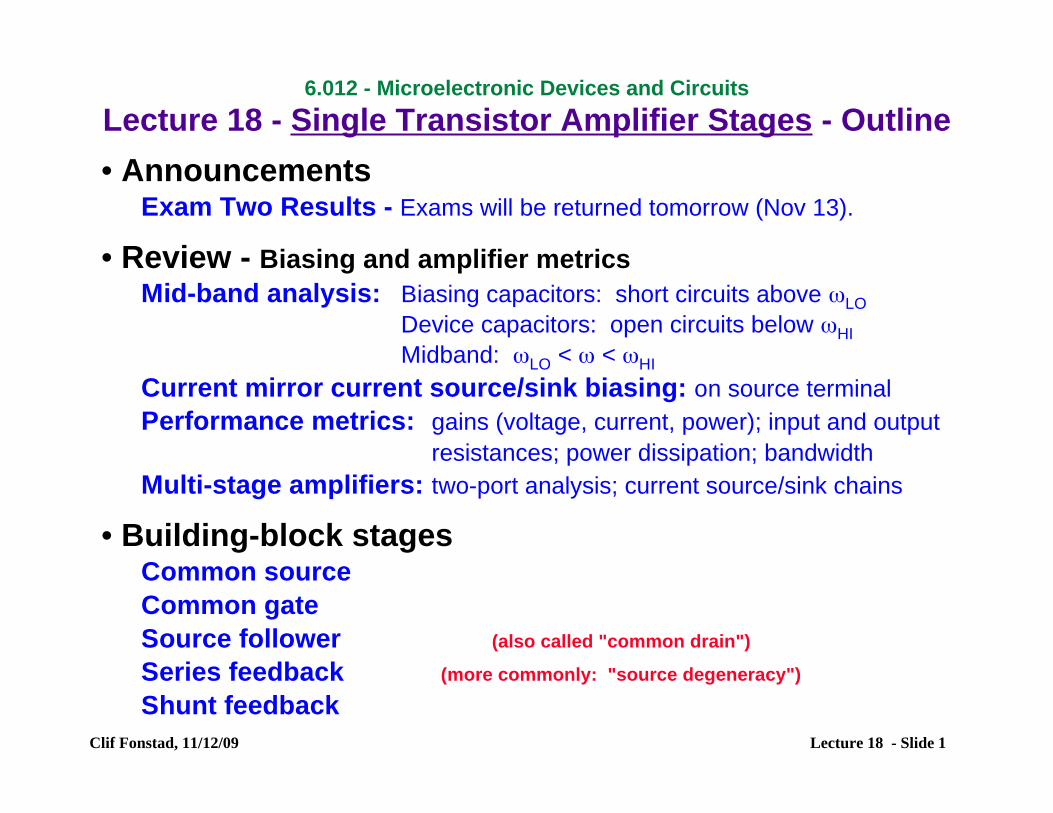
Mid-band: the frequency range of constant gain and phase
IBIAS
V-
V+
vout
+
-vin
+
-
CE
CO
g!
+
-
v!
+
-
v in
v t
+
-
rtgmv! go
+
-
voutgLOAD
rIBIAS
CE
COCµ
C!gnext
Common emitter
example:
Biasing capacitors: effective shorts ω > ωLO Device capacitors: effective open circuits ω < ωHI
We call the frequency range between ωLO and ωHI, the "mid-band" range. For frequencies in this range our model is simply:
g!
+
-
v!gmv! go gl
+
-
v in
+
-
voutv t
+
-
rt(≡ gLOAD
+ gnext)ωLO<ω<ωHI
Valid for ωLO < ω < ωHI, the "mid-band" range, where all bias capacitors are shorts and all device capacitors are open. Clif Fonstad, 11/12/09 Lecture 18 - Slide 2
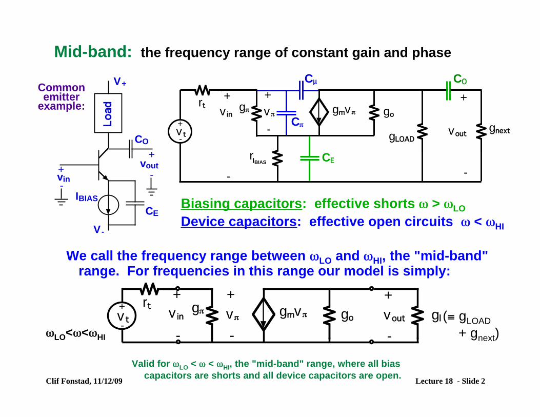
Mid-band, cont: The mid-band range of frequencies
In this range of frequencies the gain is a constant, and thephase shift between the input and output is also constant(either 0˚ or 180˚).
log !
log |A vd |
!b !c!d!a
!LO !LO*
!4 !5!2!1 !3
!HI* !HI
Mid-band Range
All of the parasitic and intrinsic device capacitancesare effectively open circuits
All of the biasing and coupling capacitors are effectively short circuits
* We will learn how to estimate ωHI and ωLO in Lectures 23/24. Clif Fonstad, 11/12/09 Lecture 18 - Slide 3
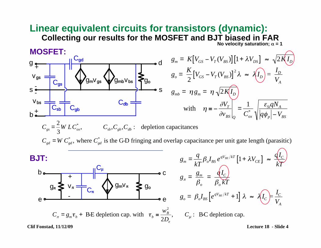
Linear equivalent circuits for transistors (dynamic):Collecting our results for the MOSFET and BJT biased in FAR
No velocity saturation; α = 1
MOSFET:
BJT:
+
-Cgs
vgs
g
s
Cgd
gmbvbs go
s
d
gmvgs
b
-
+
vbs
Csb
CdbCgb
!
gm = K VGS "VT (VBS )[ ] 1+ #VDS[ ] $ 2K ID
go =K
2VGS "VT (VBS )[ ]
2# $ # ID =
ID
VA
gmb = %gm = % 2K ID
with % & "'VT
'vBS Q
=1
Cox
*
(SiqNA
q)p "VBS
!
Cgs =2
3W LCox
*, Csb ,Cgb ,Cdb : depletion capacitances
Cgd = W Cgd
*, where Cgd
* is the G-D fringing and overlap capacitance per unit gate length (parasitic)
+
-
g!C!
v!
b
e
Cµ
gmv! go
e
c
!
gm =q
kT"oIBS e
qVBE kT1+ #VCE[ ] $
q IC
kT
g% =gm
"o
=q IC
"o kT
go = "oIBS eqVBE kT +1[ ] # $ # IC =
IC
VA
!
C" = gm# b + B-E depletion cap. with # b $wB
2
2De
, Cµ : B-C depletion cap.
Clif Fonstad, 11/12/09 Lecture 18 - Slide 4
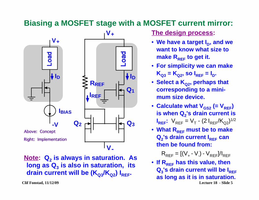
Biasing a MOSFET stage with a MOSFET current mirror:
Clif Fonstad, 11/12/09
Note: Q2 is always in saturation. As long as Q3 is also in saturation, its drain current will be (KQ3/KQ2) IREF.
Above: Concept
Right: Implementation
V-
Q2 Q3
V+
RREF
Q1
ID
IREF
IBIAS
-V
ID
V+
The design process: • We have a target ID, and we
want to know what size to make RREF to get it.
• For simplicity we can make KQ3 = KQ2, so IREF = ID.
• Select a KQ2, perhaps that corresponding to a mini-mum size device.
• Calculate what VGS2 (= VREF) is when Q2's drain current is IREF: VREF = VT - (2 IREF/KQ2)1/2
• What RREF must be to make Q2's drain current IREF can then be found from:
RREF = [(V+ - V )- - VREF]/IREF
• If RREF has this value, then Q3's drain current will be IREF as long as it is in saturation.
Lecture 18 - Slide 5
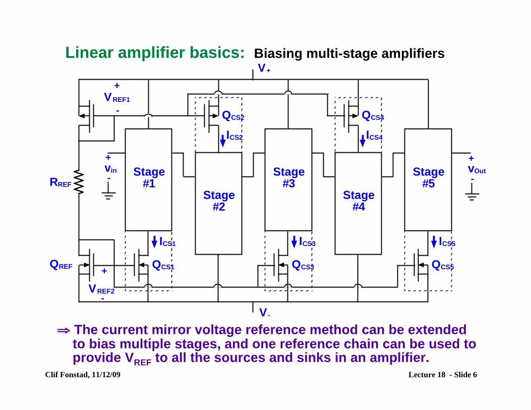
QREF+
RREF
V+
V-
ICS1
QCS1
VREF2
-
Stage
#1
ICS2
QCS2
Stage
#2
ICS3
QCS3
Stage
#3
ICS5
QCS5
Stage
#5
vin
+
-vOut
+
-
ICS4
QCS4
+
VREF1
-
Stage
#4
Linear amplifier basics: Biasing multi-stage amplifiers
⇒ The current mirror voltage reference method can be extendedto bias multiple stages, and one reference chain can be used toprovide VREF to all the sources and sinks in an amplifier.
Clif Fonstad, 11/12/09 Lecture 18 - Slide 6
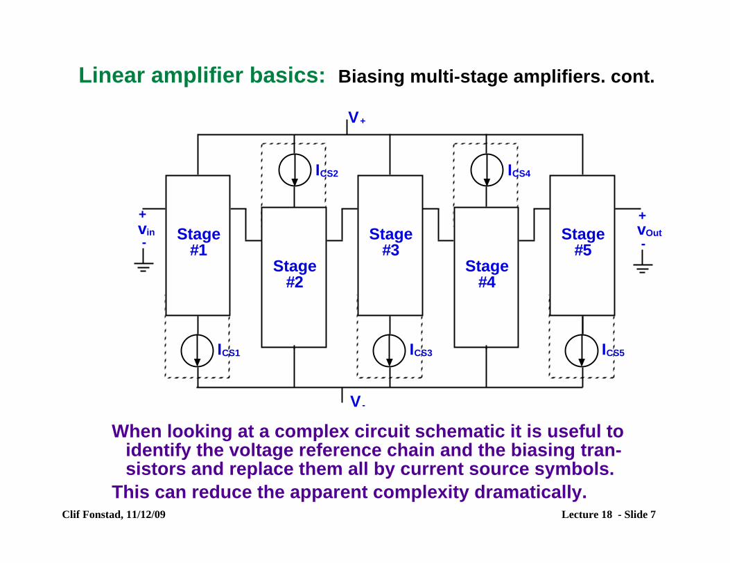
Linear amplifier basics: Biasing multi-stage amplifiers. cont.
V+
V-
ICS1
Stage
#1
ICS2
Stage
#2
ICS3
Stage
#3
Stage
#4
ICS5
Stage
#5
vin
+
-vOut
+
-
ICS4
When looking at a complex circuit schematic it is useful toidentify the voltage reference chain and the biasing tran-sistors and replace them all by current source symbols.
This can reduce the apparent complexity dramatically. Clif Fonstad, 11/12/09 Lecture 18 - Slide 7
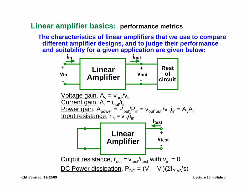
Linear amplifier basics: performance metrics
The characteristics of linear amplifiers that we use to comparedifferent amplifier designs, and to judge their performanceand suitability for a given application are given below:
Linear
Amplifier
+ +
--
vin
ioutiin
vout
Rest
of
circuit
Voltage gain, Av = vout/vin Current gain, Ai = iout/iin Power gain, Apower = Pout/Pin = voutiout /viniin = AvAi
DC Power dissipation, PDC = (V+ - V-)(ΣIBIAS 's)
Input resistance, rin = vin/iin
Linear
Amplifier
+
-
itest
vtest
Output resistance, rout = vtest/itest with vin = 0
Clif Fonstad, 11/12/09 Lecture 18 - Slide 8
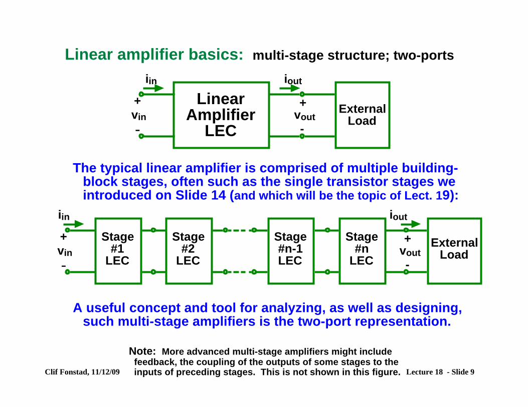
Linear amplifier basics: multi-stage structure; two-ports
Linear
Amplifier
LEC
+ +
--
vin
ioutiin
voutExternal
Load
The typical linear amplifier is comprised of multiple building-block stages, often such as the single transistor stages weintroduced on Slide 14 (and which will be the topic of Lect. 19):
External
Load
+ +
--
vin
ioutiin
vout
Stage
#n
LEC
Stage
#1
LEC
Stage
#2
LEC
Stage
#n-1
LEC
A useful concept and tool for analyzing, as well as designing,such multi-stage amplifiers is the two-port representation.
Note: More advanced multi-stage amplifiers might includefeedback, the coupling of the outputs of some stages to the
Clif Fonstad, 11/12/09 inputs of preceding stages. This is not shown in this figure. Lecture 18 - Slide 9
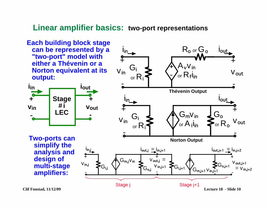
Linear amplifier basics: two-port representations
Each building block stagecan be represented by a"two-port" model witheither a Thévenin or a Norton equivalent at its
+ +
--
vin
ioutiin
vout
Stage
# i
LEC
output: Avv in
or Rfiin
Ro or Go
+
-
v in
+
-
vout
iin iout
+
-Gi
or R i
Gmv in
or A iiin
+
-
v in
+
-
vout
iin iout
Go
or Ro
Gi
or R i
Norton Output
Thévenin Output
Two-ports cansimplify theanalysis anddesign ofmulti-stageamplifiers:
Gm,jv in
+
-
v in,j
+
-
vout,j =
v in,j+1
iin,j
Go,jGi,j
iout,j = iin,j+1
+
-
vout,j+1
= v in,j+2
iout,j+1 = iin,j+2
Go,j+1Gi,j+1Gm,j+1v in,j+1
Stage j Stage j+1 Clif Fonstad, 11/12/09 Lecture 18 - Slide 10
IBIAS
-V
+V
1
2
3
IBIAS
-V
+V
1
2
3
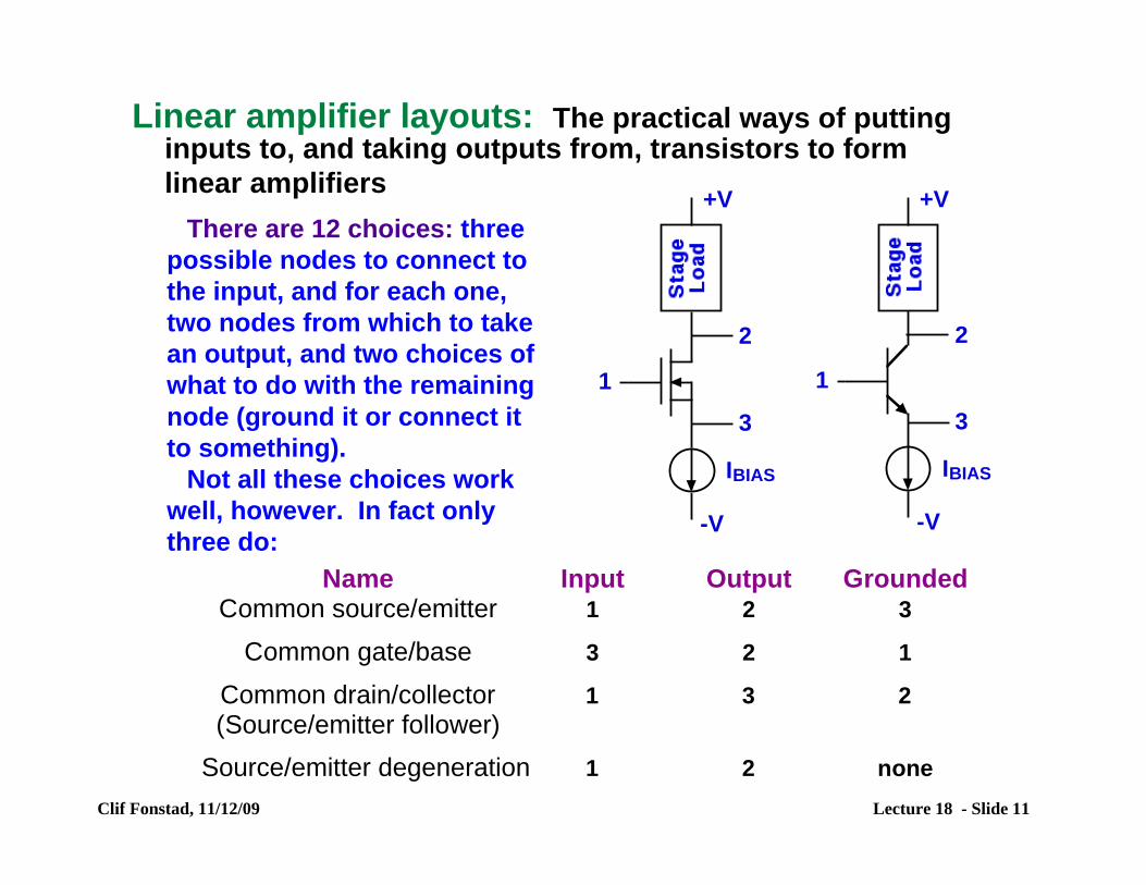
Linear amplifier layouts: The practical ways of puttinginputs to, and taking outputs from, transistors to form linear amplifiers
There are 12 choices: three possible nodes to connect to the input, and for each one, two nodes from which to take an output, and two choices of what to do with the remaining node (ground it or connect it to something).
Not all these choices work well, however. In fact only three do:
Name Input Output Grounded Common source/emitter 1 2 3
Common gate/base 3 2 1
Common drain/collector 1 3 2 (Source/emitter follower)
Source/emitter degeneration 1 2 none Clif Fonstad, 11/12/09 Lecture 18 - Slide 11
IBIAS
V-
V+
vout
+
-vin
+
-
CE
CO
IBIAS
V-
V+
vout
+
-
vIN
+
-
CO
CI
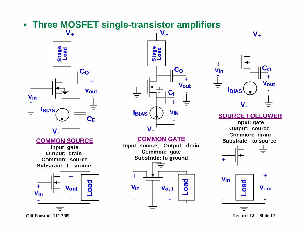
• Three MOSFET single-transistor amplifiers
V-
IBIAS
V+
vout +
-
vin +
-
CO
SOURCE FOLLOWER Input: gate
Output: source Common: drain
Substrate: to source
IBIAS
V-
V+
vin
+
-
CE
CO
vout
+
-
COMMON SOURCE Input: gate
Output: drainCommon: source
Substrate: to source
IBIAS
V-
V+
vout
+
-
vIN
+
-
CO
CI
COMMON GATE Input: source; Output: drain
Common: gate Substrate: to ground
vout
+
-
vin
+
-
vout
+
-vin +
-
vout
+
-
vin
+
-
Clif Fonstad, 11/12/09 Lecture 18 - Slide 12
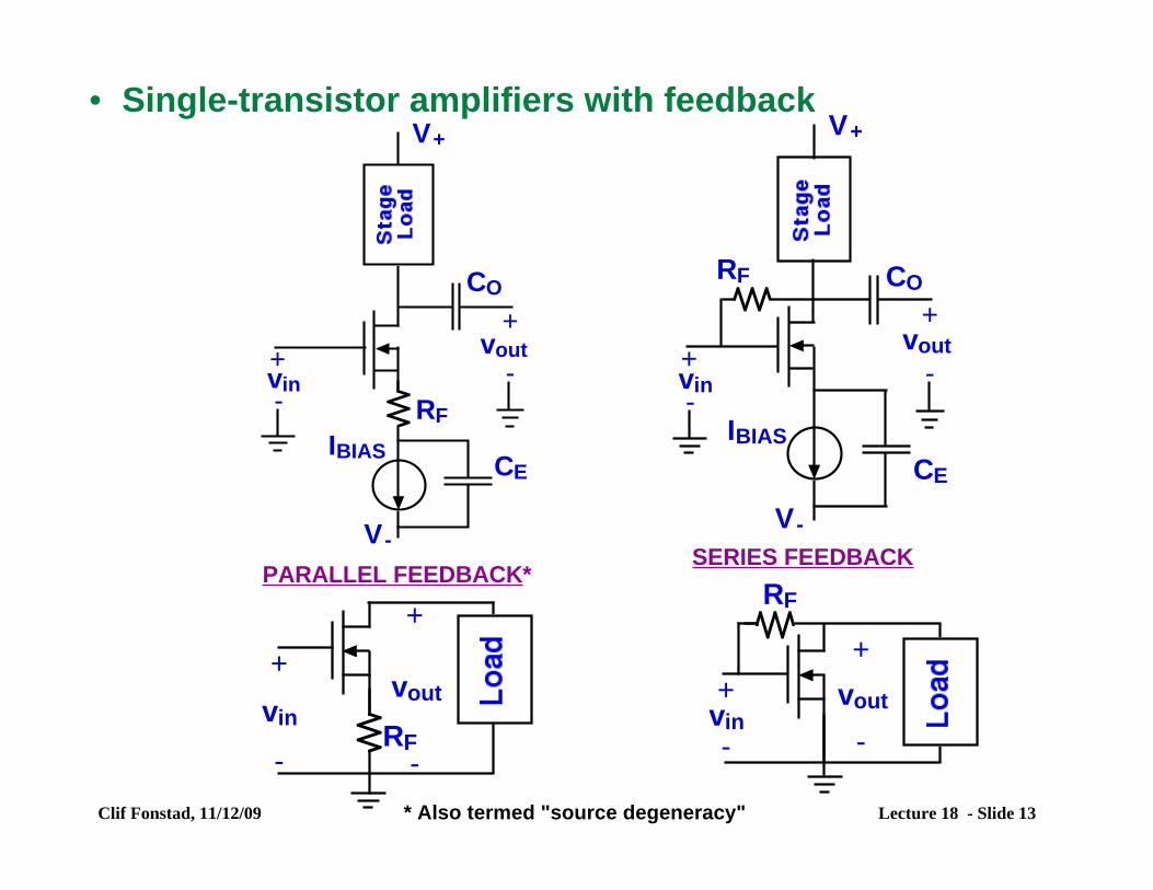
• Single-transistor amplifiers with feedbackV+
+
vin +
CO RF CO
+ voutvout
+- -vin
- -RF IBIAS
IBIAS CE CE
V-V-
SERIES FEEDBACK
V+
Clif Fonstad, 11/12/09 Lecture 18 - Slide 13
PARALLEL FEEDBACK*
vout
+
-vin
+
-
RF
vout
+
-
vin
+
-RF
* Also termed "source degeneracy"
IBIAS
V-
V+
+
vin
+
-
CE
CO
vout
+
-
External
Load
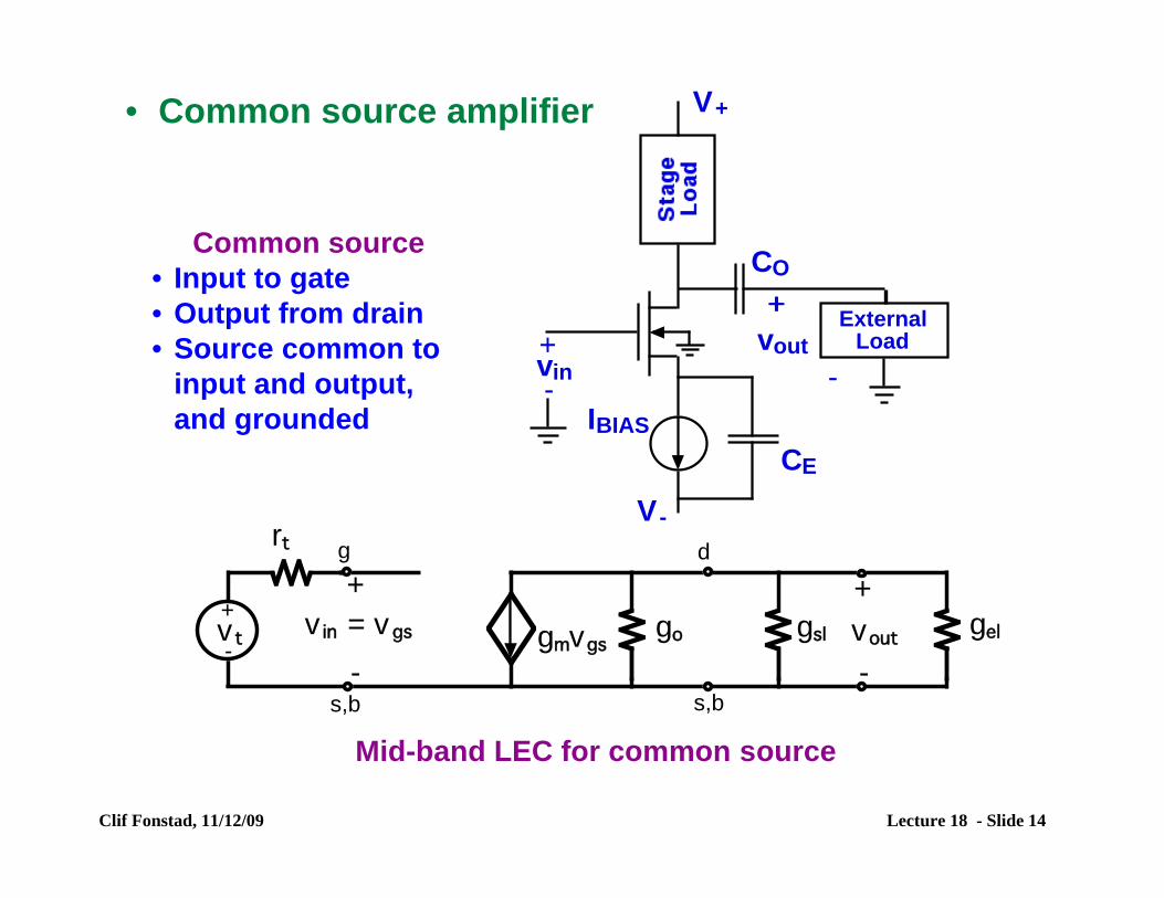
• Common source amplifier
Common source • Input to gate • Output from drain • Source common to
input and output, and grounded
gmvgsgo
d
s,bs,b
g
gsl
+
-
v in = v gsv t
+
-
rt
+
-
voutgel
Mid-band LEC for common source
Clif Fonstad, 11/12/09 Lecture 18 - Slide 14
Common source amplifier, cont.
gmvgsgo
d
s,bs,b
g
gsl
+
-
v in = v gsv t
+
-
rt
+
-
voutgel
!
vout = "gmvin
go + gsl + gel
= "gmvt
go + gsl + gel
a large |#|
!
Av = "gm
go + gsl
=Gm
Go
#
$ %
&
' (
Two-ports:
Gmv in
+
-
v in
+
-
vout
iin iout
GoGi
Avv in
Ro
+
-
v in
+
-
vout
iin iout
+
-Gi
!
Go = go + gsl( )
!
Gi = 0 Ri ="( )
!
Gm = "gm
A good workhorse gain stage Clif Fonstad, 11/12/09 Lecture 18 - Slide 15
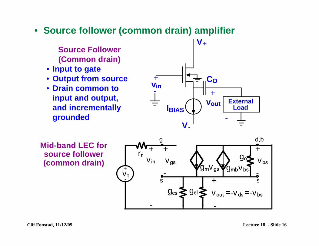
• Source follower (common drain) amplifier
Source Follower (Common drain)
• Input to gate • Output from source • Drain common to
input and output, and incrementally grounded
IBIAS
V-
V+
vout
+
vin
+
-
CO
-
External
Load
+
-
vgsgmvgs
go
gcs
+
-
v in
+
-
vout=-vds =-vbs
v t
+
-
rt
d,b
s
g
s
gel
gmbvbs
+
-
vbs
Mid-band LEC for source follower (common drain)
Clif Fonstad, 11/12/09 Lecture 18 - Slide 16
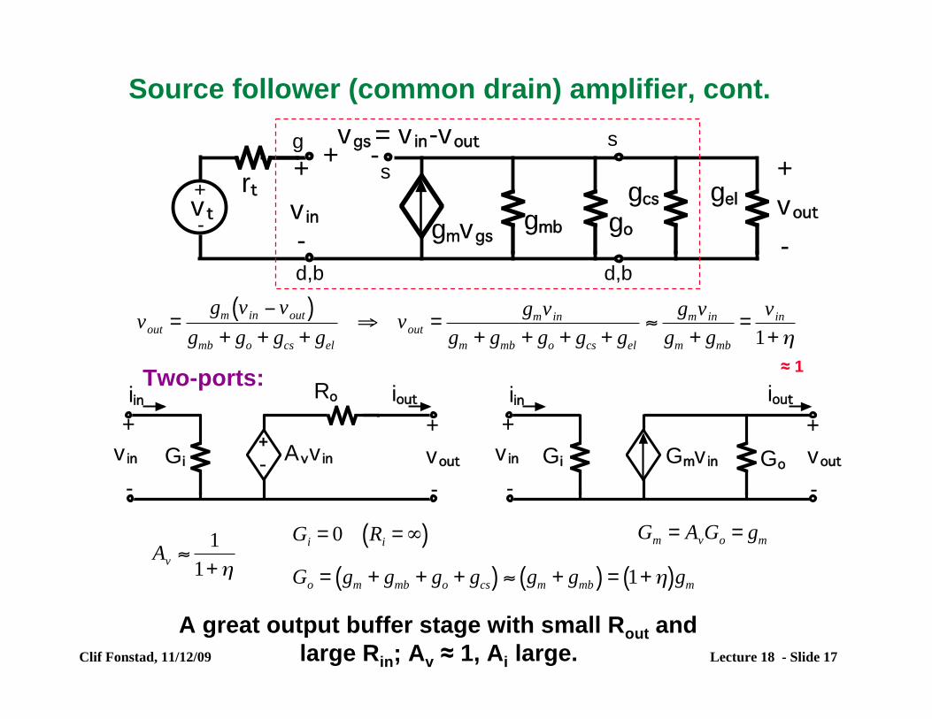
Two-ports:
Avv in
Ro
+
-
v in
+
-
vout
iin iout
+
-Gi
Source follower (common drain) amplifier, cont. vgs= v in-vout
gcs
- -
voutgel
+ -
gmvgsgo
+
v in
+
v t
+
-
rt
d,b
sg
s
gmb
d,b
!
vout =gm vin " vout( )
gmb + go + gcs + gel
# vout =gmvin
gm + gmb + go + gcs + gel
$gmvin
gm + gmb
=vin
1+%
!
Av "1
1+#
!
Go = gm + gmb + go + gcs( ) " gm + gmb( ) = 1+#( )gm
!
Gi = 0 Ri ="( )
!
Gm = AvGo = gm
Gmv in
+
-
v in
+
-
vout
iin iout
GoGi
≈ 1
A great output buffer stage with small Rout and Clif Fonstad, 11/12/09 large Rin; Av ≈ 1, Ai large. Lecture 18 - Slide 17
Clif Fonstad, 11/12/09 Lecture 18 - Slide 18
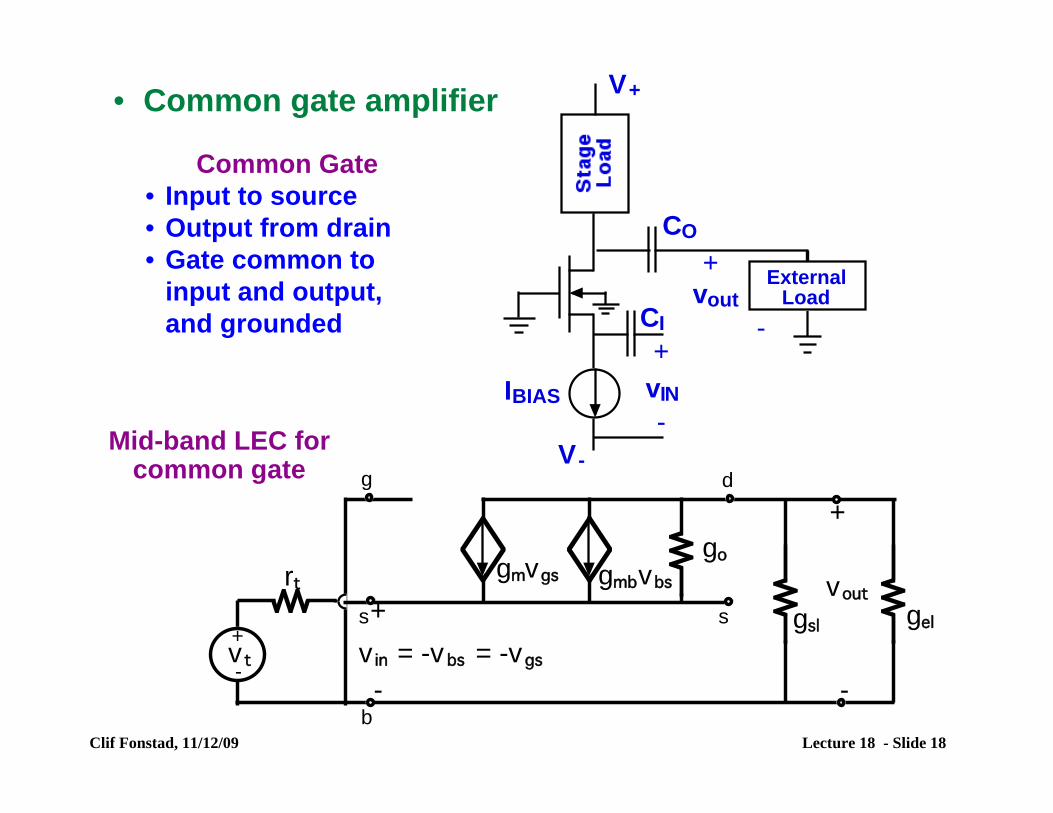
• Common gate amplifier
Common Gate • Input to source • Output from drain • Gate common to
input and output, and grounded
IBIAS
V-
V+
vout
+
-
vIN
+
-
CO
CI
External
Load
Mid-band LEC for common gate
gmvgs
go
d
ss
g
gsl+
-
v in = -v bs = -vgsv t
+
-
rt
+
-
vout
gel
b
gmbvbs
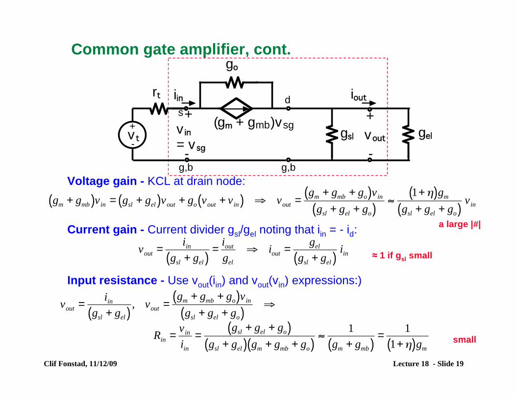
Common gate amplifier, cont.
!
gm + gmb( )vin = gsl + gel( )vout + go vout + vin( ) " vout =gm + gmb + go( )vin
gsl + gel + go( )#
1+$( )gm
gsl + gel + go( )vin
Voltage gain - KCL at drain node:
(gm + gmb)vsg
go
+
-
v in
= v sg
v t
+
-
rt
gsl
+
-
vout gel
g,b g,b
d
s
ioutiin
a large |#| Current gain - Current divider gsl/gel noting that iin = - id:
!
vout =iin
gsl + gel( )=
iout
gel
" iout =gel
gsl + gel( )iin ≈ 1 if gsl small
Input resistance - Use vout(iin) and vout(vin) expressions:)
!
vout =iin
gsl + gel( ), vout =
gm + gmb + go( )vin
gsl + gel + go( )"
small
!
Rin =vin
iin=
gsl + gel + go( )gsl + gel( ) gm + gmb + go( )
"1
gm + gmb( )=
1
1+#( )gm
Clif Fonstad, 11/12/09 Lecture 18 - Slide 19
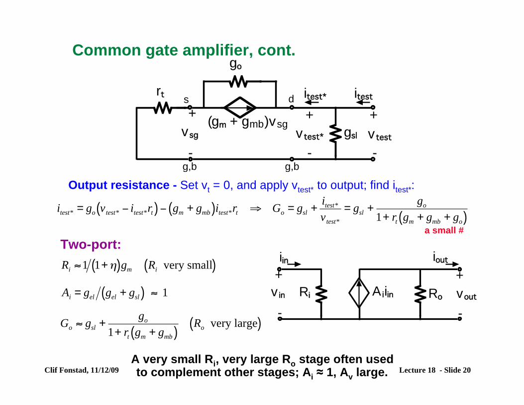
Common gate amplifier, cont.
(gm + gmb)vsg
go
+
-
vsg
rt
gsl
+
-
v test
g,b g,b
dsitest
+
-
v test*
itest*
Output resistance - Set vt = 0, and apply vtest* to output; find itest*:
a small #
!
itest* = go vtest* " itest*rt( ) " gm + gmb( )itest*rt # Go = gsl +itest*
vtest*
= gsl +go
1+ rt gm + gmb + go( )
Two-port:
!
Go " gsl +go
1+ rt gm + gmb( )Ro very large( )
!
Ri "1 1+#( )gm Ri very small( )
!
Ai = gel gel + gsl( ) " 1 A iiin
+
-
v in
+
-
vout
iin iout
RoRi
A very small Ri, very large Ro stage often usedClif Fonstad, 11/12/09 Lecture 18 - Slide 20 to complement other stages; Ai ≈ 1, Av large.
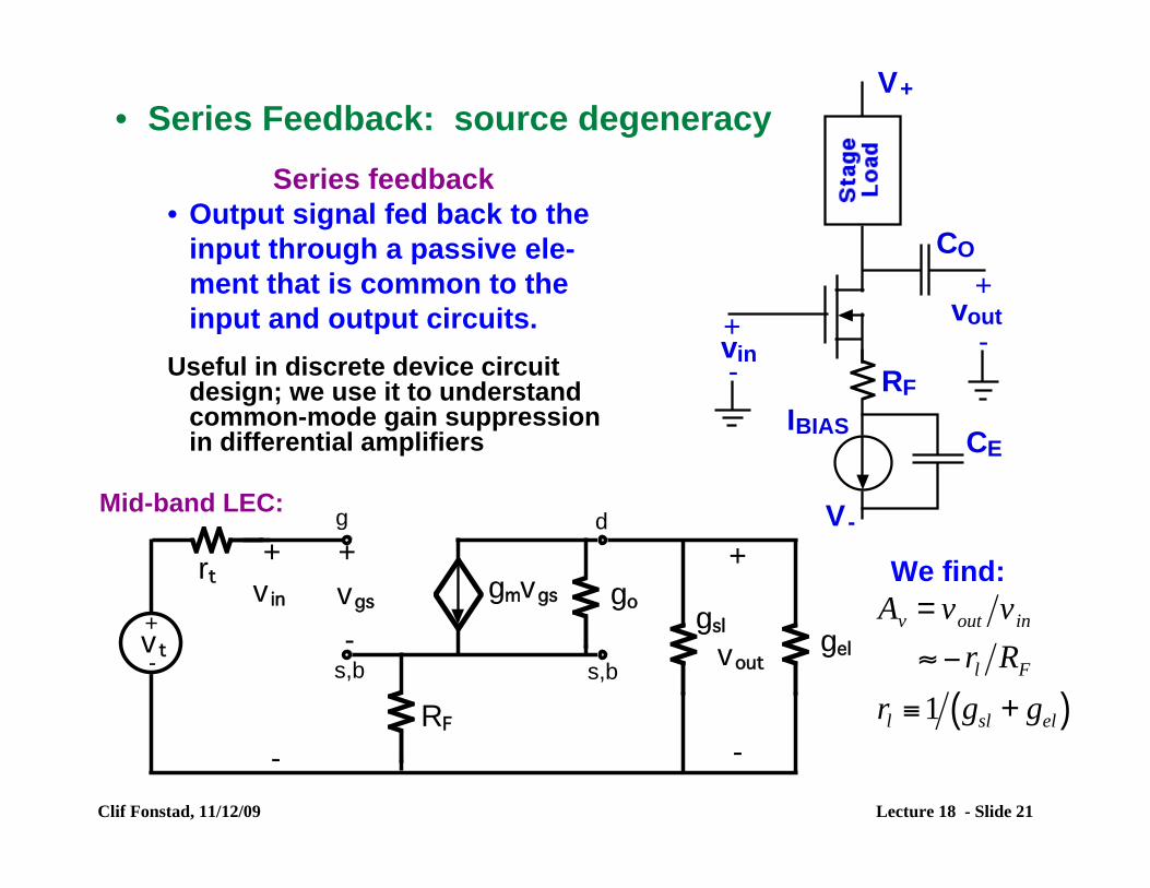
• Series Feedback: source degeneracy
Useful in discrete device circuit design; we use it to understandcommon-mode gain suppressionin differential amplifiers
IBIAS
V-
V+
vout +
-vin +
-
CE
CO
RF
Series feedback • Output signal fed back to the
input through a passive ele-ment that is common to the input and output circuits.
Mid-band LEC:
+
-
vgsgmvgs go
gsl
+
-
v in
+
-
voutv t
+
-
rt
RF
gel
s,b
g
s,b
d
!
Av = vout vin
" # rl RF
rl $1 gsl + gel( )
We find:
Clif Fonstad, 11/12/09 Lecture 18 - Slide 21
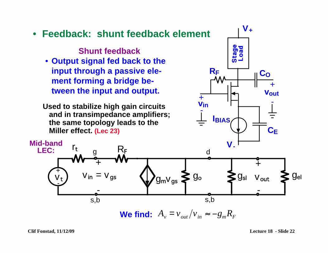
• Feedback: shunt feedback element
Used to stabilize high gain circuitsand in transimpedance amplifiers;the same topology leads to theMiller effect. (Lec 23)
IBIAS
V-
V+
vout -vin
+
-
CE
+ CO
RF
Shunt feedback • Output signal fed back to the
input through a passive ele-ment forming a bridge be-tween the input and output.
gmvgsgo
d
s,bs,b
g
gsl
+
-
v in = v gsv t
+
-
rt
+
-
voutgel
RF
!
Av = vout vin " #gmRFWe find:
Mid-band LEC:
Clif Fonstad, 11/12/09 Lecture 18 - Slide 22
• Summary of the single transistor stages (MOSFET)
!
MOSFETVoltage
gain, Av
Current
gain, Ai
Input
resistance, Ri
Output
resistance, Ro
Common source "gm
go + gl[ ]= "gmrl
'( ) # # ro =1
go
$
% &
'
( )
Common gate * gm + gmb[ ] rl
' *1 *1
gm + gmb[ ]* ro 1+
gm + gmb + go[ ]gt
+ , -
. / 0
Source followergm[ ]
gm + gmb + go + gl[ ]*1 # #
1
gm + go + gl[ ]*
1
gm
Source degeneracy
(series feedback)* "
rl
RF
# # * ro
Shunt feedback "gm "GF[ ]go + GF[ ]
* "gmRF "gl
GF
1
GF 1" Av[ ]ro || RF =
1
go + GF[ ]
$
% &
'
( )
!
Power gain, Ap = Av " Ai
Note: When vbs = 0 the gmb factors should be deleted. Clif Fonstad, 11/12/09 Lecture 18 - Slide 23
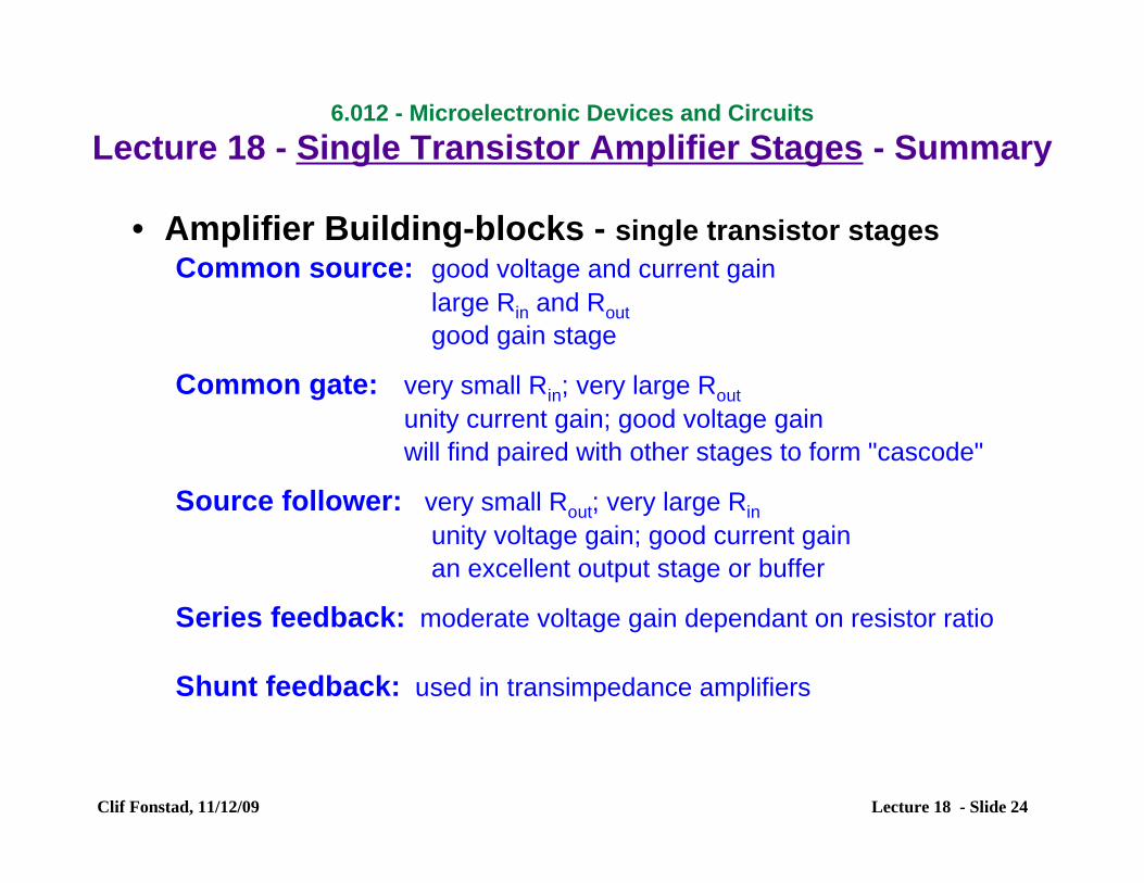
6.012 - Microelectronic Devices and Circuits
Lecture 18 - Single Transistor Amplifier Stages - Summary
• Amplifier Building-blocks - single transistor stages Common source: good voltage and current gain
large Rin and Rout good gain stage
Common gate: very small Rin; very large Rout unity current gain; good voltage gain will find paired with other stages to form "cascode"
Source follower: very small Rout; very large Rin
unity voltage gain; good current gain an excellent output stage or buffer
Series feedback: moderate voltage gain dependant on resistor ratio
Shunt feedback: used in transimpedance amplifiers
Clif Fonstad, 11/12/09 Lecture 18 - Slide 24
MIT OpenCourseWarehttp://ocw.mit.edu
6.012 Microelectronic Devices and Circuits Fall 2009
For information about citing these materials or our Terms of Use, visit: http://ocw.mit.edu/terms.