SGM8541/2/4 1.1MHz, 46μA, Rail-to-Rail I/O CMOS ...1.1MHz, 46μA, Rail-to-Rail I/O CMOS Operational...
18
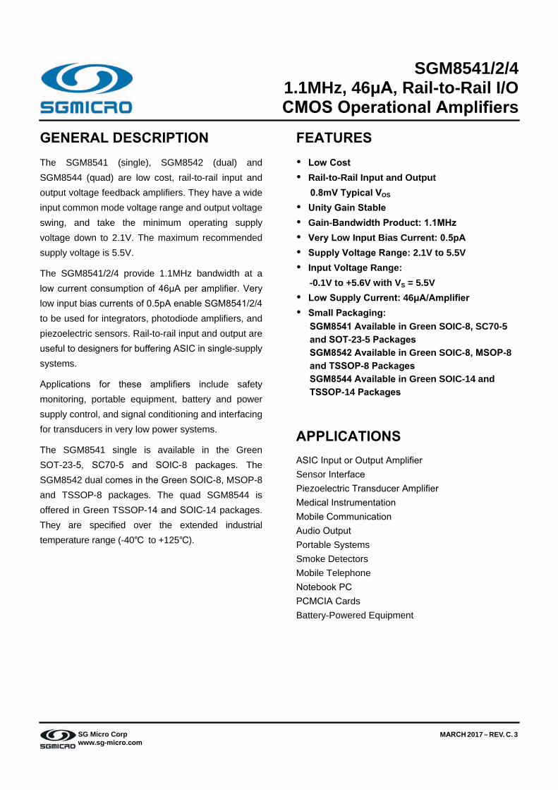
SGM8541/2/4 1.1MHz, 46μA, Rail-to-Rail I/O CMOS Operational Amplifiers MARCH 2017 – REV. C. 3 SG Micro Corp www.sg-micro.com GENERAL DESCRIPTION The SGM8541 (single), SGM8542 (dual) and SGM8544 (quad) are low cost, rail-to-rail input and output voltage feedback amplifiers. They have a wide input common mode voltage range and output voltage swing, and take the minimum operating supply voltage down to 2.1V. The maximum recommended supply voltage is 5.5V. The SGM8541/2/4 provide 1.1MHz bandwidth at a low current consumption of 46μA per amplifier. Very low input bias currents of 0.5pA enable SGM8541/2/4 to be used for integrators, photodiode amplifiers, and piezoelectric sensors. Rail-to-rail input and output are useful to designers for buffering ASIC in single-supply systems. Applications for these amplifiers include safety monitoring, portable equipment, battery and power supply control, and signal conditioning and interfacing for transducers in very low power systems. The SGM8541 single is available in the Green SOT-23-5, SC70-5 and SOIC-8 packages. The SGM8542 dual comes in the Green SOIC-8, MSOP-8 and TSSOP-8 packages. The quad SGM8544 is offered in Green TSSOP-14 and SOIC-14 packages. They are specified over the extended industrial temperature range (-40℃ to +125℃). FEATURES Low Cost Rail-to-Rail Input and Output 0.8mV Typical V OS Unity Gain Stable Gain-Bandwidth Product: 1.1MHz Very Low Input Bias Current: 0.5pA Supply Voltage Range: 2.1V to 5.5V Input Voltage Range: -0.1V to +5.6V with V S = 5.5V Low Supply Current: 46μA/Amplifier Small Packaging: SGM8541 Available in Green SOIC-8, SC70-5 and SOT-23-5 Packages SGM8542 Available in Green SOIC-8, MSOP-8 and TSSOP-8 Packages SGM8544 Available in Green SOIC-14 and TSSOP-14 Packages APPLICATIONS ASIC Input or Output Amplifier Sensor Interface Piezoelectric Transducer Amplifier Medical Instrumentation Mobile Communication Audio Output Portable Systems Smoke Detectors Mobile Telephone Notebook PC PCMCIA Cards Battery-Powered Equipment
-
Upload
vuongtuyen -
Category
Documents
-
view
216 -
download
0
Transcript of SGM8541/2/4 1.1MHz, 46μA, Rail-to-Rail I/O CMOS ...1.1MHz, 46μA, Rail-to-Rail I/O CMOS Operational...
SGM8541/2/4
1.1MHz, 46μA, Rail-to-Rail I/O CMOS Operational Amplifiers
MARCH 2017 – REV. C. 3SG Micro Corp www.sg-micro.com
GENERAL DESCRIPTION The SGM8541 (single), SGM8542 (dual) and SGM8544 (quad) are low cost, rail-to-rail input and output voltage feedback amplifiers. They have a wide input common mode voltage range and output voltage swing, and take the minimum operating supply voltage down to 2.1V. The maximum recommended supply voltage is 5.5V.
The SGM8541/2/4 provide 1.1MHz bandwidth at a low current consumption of 46μA per amplifier. Very low input bias currents of 0.5pA enable SGM8541/2/4 to be used for integrators, photodiode amplifiers, and piezoelectric sensors. Rail-to-rail input and output are useful to designers for buffering ASIC in single-supply systems.
Applications for these amplifiers include safety monitoring, portable equipment, battery and power supply control, and signal conditioning and interfacing for transducers in very low power systems.
The SGM8541 single is available in the Green SOT-23-5, SC70-5 and SOIC-8 packages. The SGM8542 dual comes in the Green SOIC-8, MSOP-8 and TSSOP-8 packages. The quad SGM8544 is offered in Green TSSOP-14 and SOIC-14 packages. They are specified over the extended industrial temperature range (-40℃ to +125℃).
FEATURES Low Cost Rail-to-Rail Input and Output
0.8mV Typical VOS Unity Gain Stable Gain-Bandwidth Product: 1.1MHz Very Low Input Bias Current: 0.5pA Supply Voltage Range: 2.1V to 5.5V Input Voltage Range:
-0.1V to +5.6V with VS = 5.5V Low Supply Current: 46μA/Amplifier Small Packaging:
SGM8541 Available in Green SOIC-8, SC70-5 and SOT-23-5 Packages SGM8542 Available in Green SOIC-8, MSOP-8 and TSSOP-8 Packages SGM8544 Available in Green SOIC-14 and TSSOP-14 Packages
APPLICATIONS ASIC Input or Output Amplifier Sensor Interface Piezoelectric Transducer Amplifier Medical Instrumentation Mobile Communication Audio Output Portable Systems Smoke Detectors Mobile Telephone Notebook PC PCMCIA Cards Battery-Powered Equipment
1.1MHz, 46μA, Rail-to-Rail I/O SGM8541/2/4 CMOS Operational Amplifiers
2
MARCH 2017 SG Micro Corp www.sg-micro.com
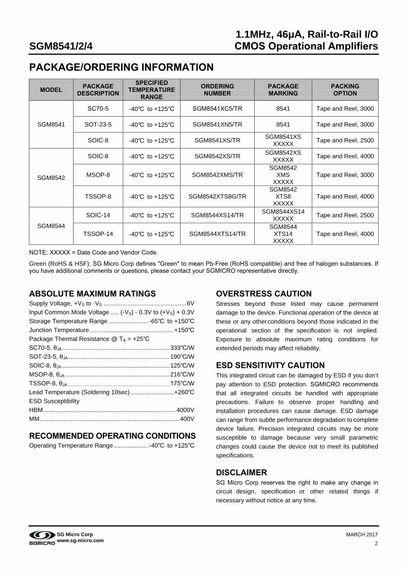
PACKAGE/ORDERING INFORMATION
MODEL PACKAGE DESCRIPTION
SPECIFIED TEMPERATURE
RANGE ORDERING NUMBER
PACKAGE MARKING
PACKING OPTION
SGM8541
SC70-5 -40℃ to +125℃ SGM8541XC5/TR 8541 Tape and Reel, 3000
SOT-23-5 -40℃ to +125℃ SGM8541XN5/TR 8541 Tape and Reel, 3000
SOIC-8 -40℃ to +125℃ SGM8541XS/TR SGM8541XS XXXXX Tape and Reel, 2500
SGM8542
SOIC-8 -40℃ to +125℃ SGM8542XS/TR SGM8542XS XXXXX Tape and Reel, 4000
MSOP-8 -40℃ to +125℃ SGM8542XMS/TR SGM8542
XMS XXXXX
Tape and Reel, 3000
TSSOP-8 -40℃ to +125℃ SGM8542XTS8G/TR SGM8542
XTS8 XXXXX
Tape and Reel, 4000
SGM8544
SOIC-14 -40℃ to +125℃ SGM8544XS14/TR SGM8544XS14 XXXXX Tape and Reel, 2500
TSSOP-14 -40℃ to +125℃ SGM8544XTS14/TR SGM8544
XTS14 XXXXX
Tape and Reel, 4000
NOTE: XXXXX = Date Code and Vendor Code.
Green (RoHS & HSF): SG Micro Corp defines "Green" to mean Pb-Free (RoHS compatible) and free of halogen substances. If you have additional comments or questions, please contact your SGMICRO representative directly.
ABSOLUTE MAXIMUM RATINGS Supply Voltage, +VS to -VS ................................................ 6V Input Common Mode Voltage ..... (-VS) - 0.3V to (+VS) + 0.3V Storage Temperature Range ....................... -65℃ to +150℃ Junction Temperature ................................................. +150℃ Package Thermal Resistance @ TA = +25℃ SC70-5, θJA .............................................................. 333℃/W SOT-23-5, θJA .......................................................... 190℃/W SOIC-8, θJA .............................................................. 125℃/W MSOP-8, θJA ............................................................ 216℃/W TSSOP-8, θJA ......................................................................................... 175℃/W Lead Temperature (Soldering 10sec) ......................... +260℃ ESD Susceptibility HBM ............................................................................. 4000V MM ................................................................................. 400V RECOMMENDED OPERATING CONDITIONS Operating Temperature Range ................... .-40℃ to +125℃
OVERSTRESS CAUTION Stresses beyond those listed may cause permanent damage to the device. Functional operation of the device at these or any other conditions beyond those indicated in the operational section of the specification is not implied. Exposure to absolute maximum rating conditions for extended periods may affect reliability. ESD SENSITIVITY CAUTION This integrated circuit can be damaged by ESD if you don’t pay attention to ESD protection. SGMICRO recommends that all integrated circuits be handled with appropriate precautions. Failure to observe proper handling and installation procedures can cause damage. ESD damage can range from subtle performance degradation to complete device failure. Precision integrated circuits may be more susceptible to damage because very small parametric changes could cause the device not to meet its published specifications. DISCLAIMER SG Micro Corp reserves the right to make any change in circuit design, specification or other related things if necessary without notice at any time.
1.1MHz, 46μA, Rail-to-Rail I/O SGM8541/2/4 CMOS Operational Amplifiers
3
MARCH 2017 SG Micro Corp www.sg-micro.com
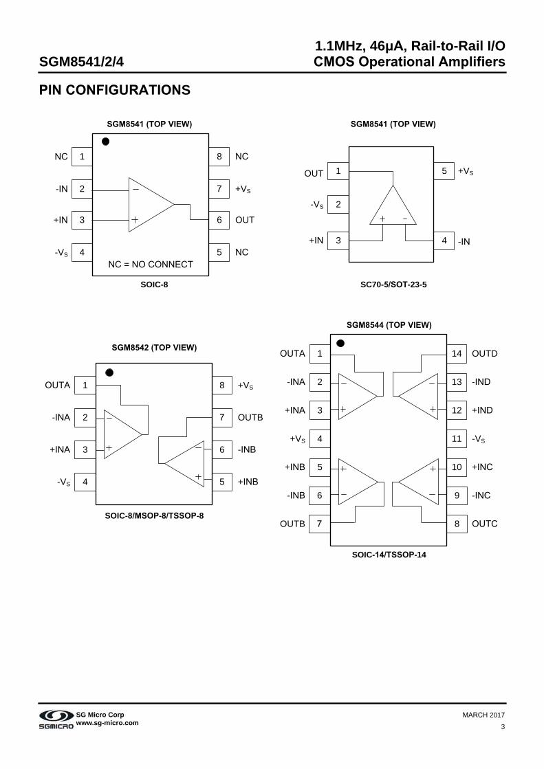
PIN CONFIGURATIONS
SGM8541 (TOP VIEW) SGM8541 (TOP VIEW)
5
6
7
81
2
3
4
+VS
NCNC = NO CONNECT
-IN
+IN
-VS
NC NC
OUT
+VS
-IN3 4
51
2-VS
OUT
+IN
SOIC-8 SC70-5/SOT-23-5
SGM8544 (TOP VIEW)
SGM8542 (TOP VIEW)
10
11
12
13
141
2
3
4
5
OUTA
-INA
+INA
-VS+VS
-IND
+IND
6
7
9
8
-INB
+INB
-INC
OUTB OUTC
+INC
OUTD
OUTA
OUTB
+INB
+VS
5
6
7
81
2
3
4
-INA
+INA
-VS
-INB
SOIC-8/MSOP-8/TSSOP-8
SOIC-14/TSSOP-14
1.1MHz, 46μA, Rail-to-Rail I/O SGM8541/2/4 CMOS Operational Amplifiers
4
MARCH 2017 SG Micro Corp www.sg-micro.com
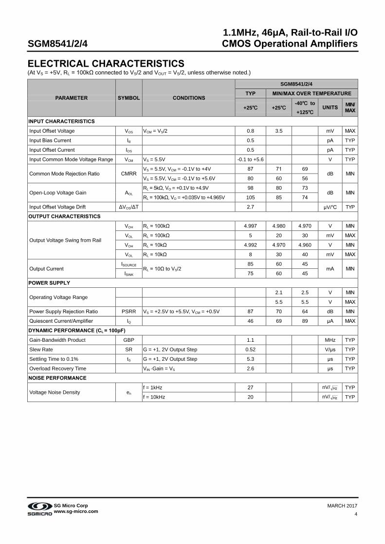
ELECTRICAL CHARACTERISTICS (At VS = +5V, RL = 100kΩ connected to VS/2 and VOUT = VS/2, unless otherwise noted.)
PARAMETER SYMBOL CONDITIONS
SGM8541/2/4
TYP MIN/MAX OVER TEMPERATURE
+25℃ +25℃ -40℃ to
+125℃ UNITS MIN/
MAX
INPUT CHARACTERISTICS
Input Offset Voltage VOS VCM = VS/2 0.8 3.5 mV MAX
Input Bias Current IB 0.5 pA TYP
Input Offset Current IOS 0.5 pA TYP
Input Common Mode Voltage Range VCM VS = 5.5V -0.1 to +5.6 V TYP
Common Mode Rejection Ratio CMRR VS = 5.5V, VCM = -0.1V to +4V 87 71 69
dB MIN VS = 5.5V, VCM = -0.1V to +5.6V 80 60 56
Open-Loop Voltage Gain AOL RL = 5kΩ, VO = +0.1V to +4.9V 98 80 73
dB MIN RL = 100kΩ, VO = +0.035V to +4.965V 105 85 74
Input Offset Voltage Drift ΔVOS/ΔT 2.7 μV/℃ TYP
OUTPUT CHARACTERISTICS
Output Voltage Swing from Rail
VOH RL = 100kΩ 4.997 4.980 4.970 V MIN
VOL RL = 100kΩ 5 20 30 mV MAX
VOH RL = 10kΩ 4.992 4.970 4.960 V MIN
VOL RL = 10kΩ 8 30 40 mV MAX
Output Current ISOURCE
RL = 10Ω to VS/2 85 60 45
mA MIN ISINK 75 60 45
POWER SUPPLY
Operating Voltage Range 2.1 2.5 V MIN
5.5 5.5 V MAX
Power Supply Rejection Ratio PSRR VS = +2.5V to +5.5V, VCM = +0.5V 87 70 64 dB MIN
Quiescent Current/Amplifier IQ 46 69 89 μA MAX
DYNAMIC PERFORMANCE (CL = 100pF)
Gain-Bandwidth Product GBP 1.1 MHz TYP
Slew Rate SR G = +1, 2V Output Step 0.52 V/μs TYP
Settling Time to 0.1% tS G = +1, 2V Output Step 5.3 μs TYP
Overload Recovery Time VIN ·Gain = VS 2.6 μs TYP
NOISE PERFORMANCE
Voltage Noise Density en f = 1kHz 27 nV/ Hz TYP
f = 10kHz 20 nV/ Hz TYP
1.1MHz, 46μA, Rail-to-Rail I/O SGM8541/2/4 CMOS Operational Amplifiers
5
MARCH 2017 SG Micro Corp www.sg-micro.com
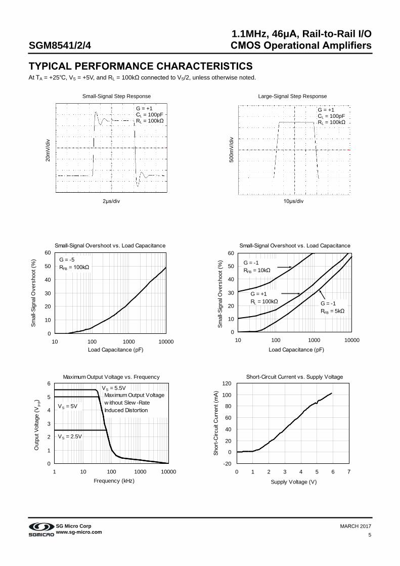
TYPICAL PERFORMANCE CHARACTERISTICS At TA = +25℃, VS = +5V, and RL = 100kΩ connected to VS/2, unless otherwise noted.
Small-Signal Step Response
2μs/div
Large-Signal Step Response
10μs/div
Small-Signal Overshoot vs. Load Capacitance
0
10
20
30
40
50
60
10 100 1000 10000Load Capacitance (pF)
Smal
l-Sig
nal O
vers
hoot
(%) G = -5
RFB = 100kΩ
Maximum Output Voltage vs. Frequency
0
1
2
3
4
5
6
1 10 100 1000 10000Frequency (kHz)
Out
put V
olta
ge (V
p-p)
Maximum Output Voltagew ithout Slew -RateInduced Distortion
VS = 5.5V
VS = 5V
VS = 2.5V
Small-Signal Overshoot vs. Load Capacitance
0
10
20
30
40
50
60
10 100 1000 10000
Load Capacitance (pF)
Smal
l-Sig
nal O
vers
hoot
(%) G = -1
RFB = 10kΩ
G = +1RL = 100kΩ G = -1
RFB = 5kΩ
Short-Circuit Current vs. Supply Voltage
-20
0
20
40
60
80
100
120
0 1 2 3 4 5 6 7
Supply Voltage (V)
Shor
t-Circ
uit C
urre
nt (m
A)
20m
V/d
iv
G = +1 CL = 100pF RL = 100kΩ
500m
V/d
iv
G = +1 CL = 100pF RL = 100kΩ
1.1MHz, 46μA, Rail-to-Rail I/O SGM8541/2/4 CMOS Operational Amplifiers
6
MARCH 2017 SG Micro Corp www.sg-micro.com
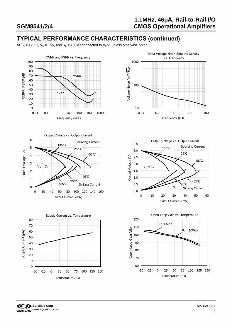
TYPICAL PERFORMANCE CHARACTERISTICS (continued) At TA = +25℃, VS = +5V, and RL = 100kΩ connected to VS/2, unless otherwise noted.
CMRR and PSRR vs. Frequency
0102030405060708090
100
0.01 0.1 1 10 100 1000 10000Frequency (kHz)
CM
RR
, PSR
R (d
B
CMRR
PSRR
Output Voltage vs. Output Current
0
1
2
3
4
5
6
0 20 40 60 80 100 120 140 160
Output Current (mA)
Out
put V
olta
ge (V
)
Sourcing Current
Sinking Current
VS = 5V
-55℃
-55℃
25℃
25℃
135℃
135℃
Supply Current vs. Temperature
0
10
20
30
40
50
60
70
80
-50 -25 0 25 50 75 100 125 150
Temperature (℃)
Supp
ly C
urre
nt (μ
A)
Input Voltage Noise Spectral Densityvs. Frequency
10
100
1000
0.01 0.1 1 10 100Frequency (kHz)
Volta
ge N
oise
(nV/√H
z)
Output Voltage vs. Output Current
0.0
0.5
1.0
1.5
2.0
2.5
3.0
3.5
0 10 20 30 40 50 60
Output Current (mA)
Out
put V
olta
ge (V
)
-55℃
25℃135℃
-55℃25℃
135℃
VS = 3V
Sourcing Current
Sinking Current
Open-Loop Gain vs. Temperature
60
70
80
90
100
110
120
-50 -25 0 25 50 75 100 125 150
Temperature (℃)
Ope
n–Lo
op G
ain
(dB)
RL = 5kΩ
RL = 100kΩ
1.1MHz, 46μA, Rail-to-Rail I/O SGM8541/2/4 CMOS Operational Amplifiers
7
MARCH 2017 SG Micro Corp www.sg-micro.com
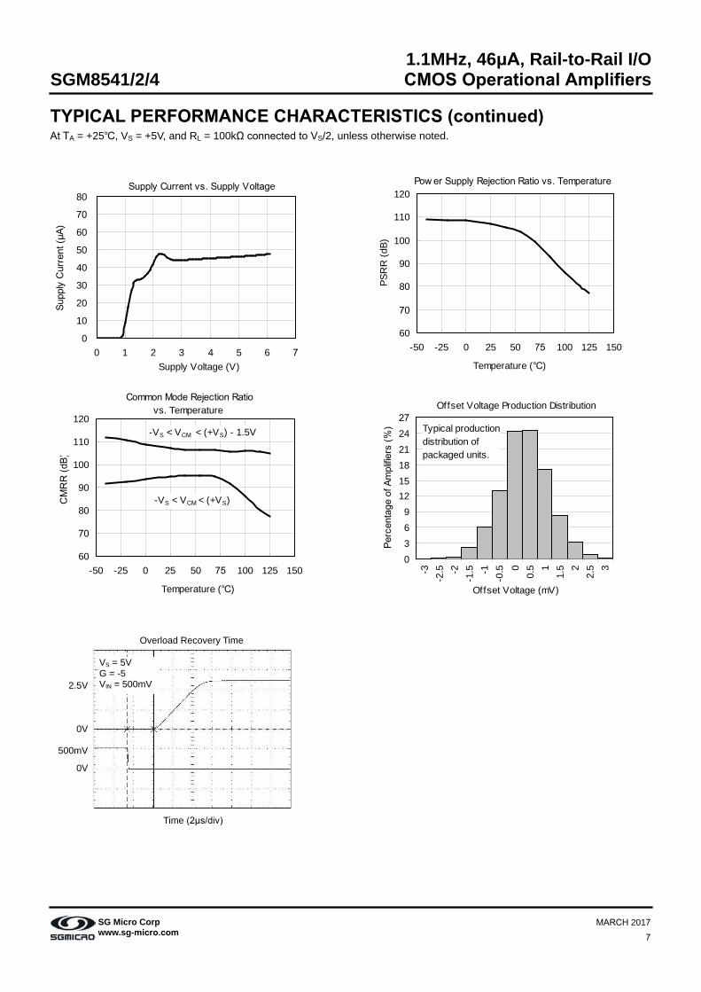
TYPICAL PERFORMANCE CHARACTERISTICS (continued) At TA = +25℃, VS = +5V, and RL = 100kΩ connected to VS/2, unless otherwise noted.
Supply Current vs. Supply Voltage
0
10
20
30
40
50
60
70
80
0 1 2 3 4 5 6 7 Supply Voltage (V)
Supp
ly C
urre
nt (μ
A)
Common Mode Rejection Ratiovs. Temperature
60
70
80
90
100
110
120
-50 -25 0 25 50 75 100 125 150
Temperature (℃)
CM
RR
(dB)
-VS < VCM < (+VS)
-VS < VCM < (+VS) - 1.5V
Overload Recovery Time
Time (2μs/div)
Pow er Supply Rejection Ratio vs. Temperature
60
70
80
90
100
110
120
-50 -25 0 25 50 75 100 125 150
Temperature (℃)
PSR
R (d
B)
Offset Voltage Production Distribution
0369
121518212427
-3-2
.5 -2-1
.5 -1-0
.5 00.
5 11.
5 22.
5 3Offset Voltage (mV)
Perc
enta
ge o
f Am
plifie
rs (%
) Typical productiondistribution ofpackaged units.
VS = 5V G = -5 VIN = 500mV
2.5V
0V
500mV
0V
1.1MHz, 46μA, Rail-to-Rail I/O SGM8541/2/4 CMOS Operational Amplifiers
8
MARCH 2017 SG Micro Corp www.sg-micro.com
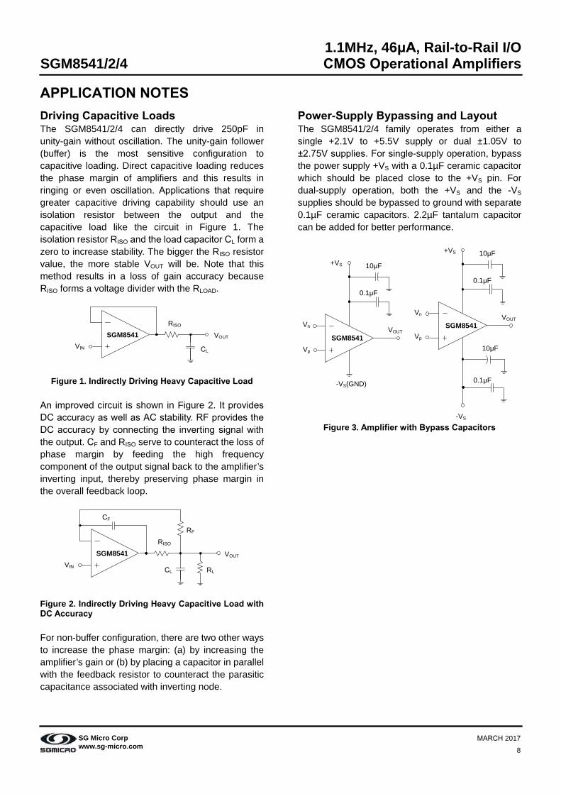
APPLICATION NOTES Driving Capacitive Loads The SGM8541/2/4 can directly drive 250pF in unity-gain without oscillation. The unity-gain follower (buffer) is the most sensitive configuration to capacitive loading. Direct capacitive loading reduces the phase margin of amplifiers and this results in ringing or even oscillation. Applications that require greater capacitive driving capability should use an isolation resistor between the output and the capacitive load like the circuit in Figure 1. The isolation resistor RISO and the load capacitor CL form a zero to increase stability. The bigger the RISO resistor value, the more stable VOUT will be. Note that this method results in a loss of gain accuracy because RISO forms a voltage divider with the RLOAD.
VIN
VOUTSGM8541
CL
RISO
Figure 1. Indirectly Driving Heavy Capacitive Load An improved circuit is shown in Figure 2. It provides DC accuracy as well as AC stability. RF provides the DC accuracy by connecting the inverting signal with the output. CF and RISO serve to counteract the loss of phase margin by feeding the high frequency component of the output signal back to the amplifier’s inverting input, thereby preserving phase margin in the overall feedback loop.
VIN
VOUTSGM8541
CL
RISO
RL
RF
CF
Figure 2. Indirectly Driving Heavy Capacitive Load with DC Accuracy For non-buffer configuration, there are two other ways to increase the phase margin: (a) by increasing the amplifier’s gain or (b) by placing a capacitor in parallel with the feedback resistor to counteract the parasitic capacitance associated with inverting node.
Power-Supply Bypassing and Layout The SGM8541/2/4 family operates from either a single +2.1V to +5.5V supply or dual ±1.05V to ±2.75V supplies. For single-supply operation, bypass the power supply +VS with a 0.1µF ceramic capacitor which should be placed close to the +VS pin. For dual-supply operation, both the +VS and the -VS supplies should be bypassed to ground with separate 0.1µF ceramic capacitors. 2.2µF tantalum capacitor can be added for better performance.
SGM8541
+VS
Vn
Vp
-VS
VOUT
10μF
0.1μF
10μF
0.1μF
SGM8541
Vn
Vp
+VS
-VS(GND)
VOUT
10μF
0.1μF
Figure 3. Amplifier with Bypass Capacitors
1.1MHz, 46μA, Rail-to-Rail I/O SGM8541/2/4 CMOS Operational Amplifiers
9
MARCH 2017 SG Micro Corp www.sg-micro.com
TYPICAL APPLICATION CIRCUITS Differential Amplifier The circuit shown in Figure 4 performs the difference function. If the resistor ratios are equal to (R4/R3 = R2/R1), then VOUT = (Vp - Vn) × R2/R1 + VREF.
Vn
Vp
VOUTSGM8541
VREF
R1
R2
R3
R4
Figure 4. Differential Amplifier
Instrumentation Amplifier The circuit in Figure 5 performs the same function as that in Figure 4 but with a high input impedance.
Vn
Vp
SGM8541
VREF
R1
R2
R3 R4
VOUT
SGM8541
SGM8541
Figure 5. Instrumentation Amplifier
Low-Pass Active Filter The low-pass filter shown in Figure 6 has a DC gain of (-R2/R1) and the -3dB corner frequency is 1/2πR2C. Make sure the filter bandwidth is within the bandwidth of the amplifier. The large values of feedback resistors can couple with parasitic capacitance and cause undesired effects such as ringing or oscillation in high-speed amplifiers. Keep resistor values as low as possible and consistent with output loading consideration.
VIN
VOUTSGM8541
R1
R2
R3 = R1 // R2
C
Figure 6. Low-Pass Active Filter
PACKAGE INFORMATION
TX00033.000 SG Micro Corp www.sg-micro.com
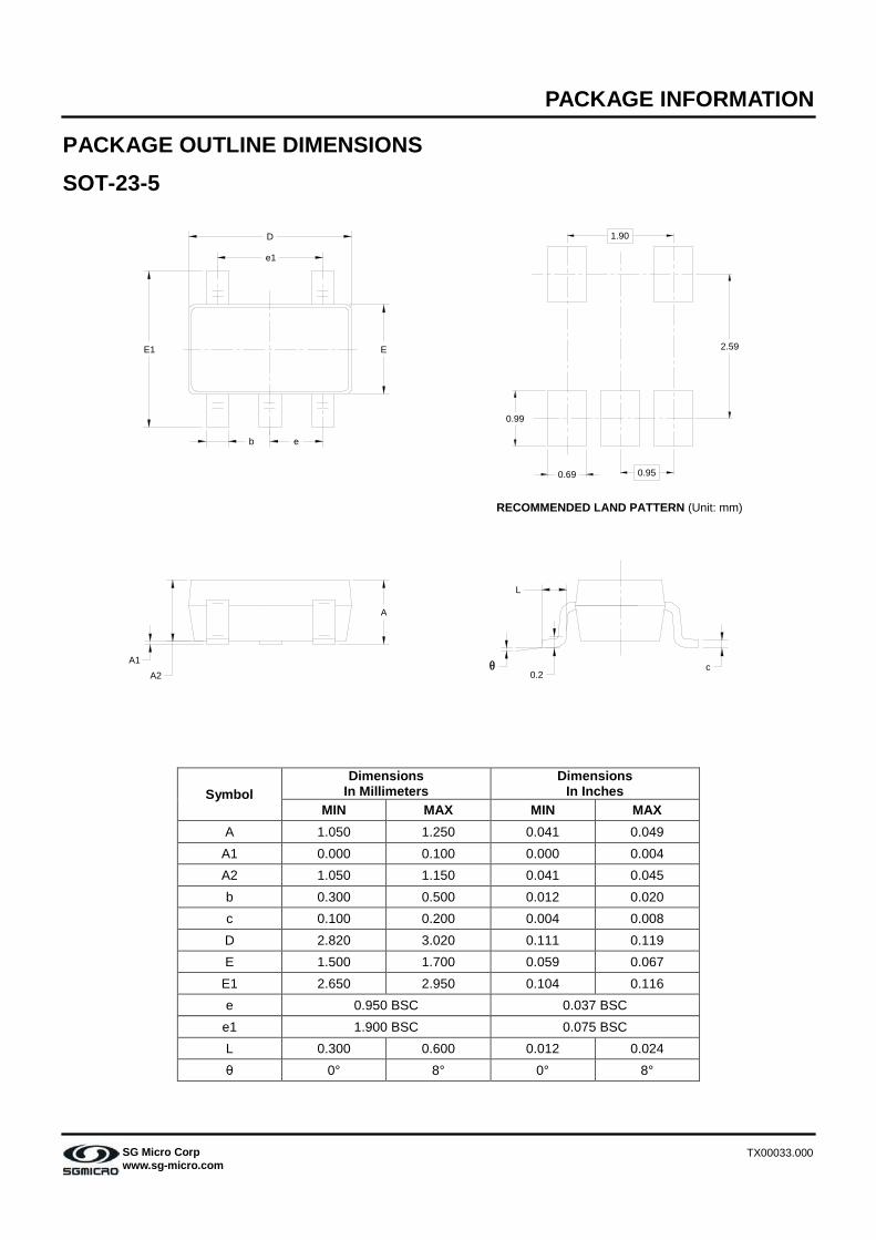
PACKAGE OUTLINE DIMENSIONS SOT-23-5
Symbol Dimensions
In Millimeters Dimensions
In Inches MIN MAX MIN MAX
A 1.050 1.250 0.041 0.049 A1 0.000 0.100 0.000 0.004 A2 1.050 1.150 0.041 0.045 b 0.300 0.500 0.012 0.020 c 0.100 0.200 0.004 0.008 D 2.820 3.020 0.111 0.119 E 1.500 1.700 0.059 0.067
E1 2.650 2.950 0.104 0.116 e 0.950 BSC 0.037 BSC
e1 1.900 BSC 0.075 BSC L 0.300 0.600 0.012 0.024 θ 0° 8° 0° 8°
EE1
e
e1
b
D
A1A2
A
c
L
θ0.2
RECOMMENDED LAND PATTERN (Unit: mm)
1.90
2.59
0.99
0.69 0.95
PACKAGE INFORMATION
TX00043.000 SG Micro Corp www.sg-micro.com
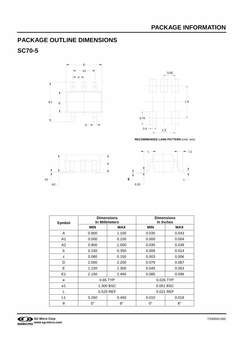
PACKAGE OUTLINE DIMENSIONS SC70-5
Symbol Dimensions
In Millimeters Dimensions
In Inches MIN MAX MIN MAX
A 0.900 1.100 0.035 0.043 A1 0.000 0.100 0.000 0.004 A2 0.900 1.000 0.035 0.039 b 0.150 0.350 0.006 0.014 c 0.080 0.150 0.003 0.006 D 2.000 2.200 0.079 0.087 E 1.150 1.350 0.045 0.053
E1 2.150 2.450 0.085 0.096 e 0.65 TYP 0.026 TYP
e1 1.300 BSC 0.051 BSC L 0.525 REF 0.021 REF
L1 0.260 0.460 0.010 0.018 θ 0° 8° 0° 8°
e
e1
E1 E
D
b
A
A2
A1
L
cθ0.20
L1
RECOMMENDED LAND PATTERN (Unit: mm)
1.9
0.65
1.3
0.75
0.4
PACKAGE INFORMATION
TX00010.000 SG Micro Corp www.sg-micro.com
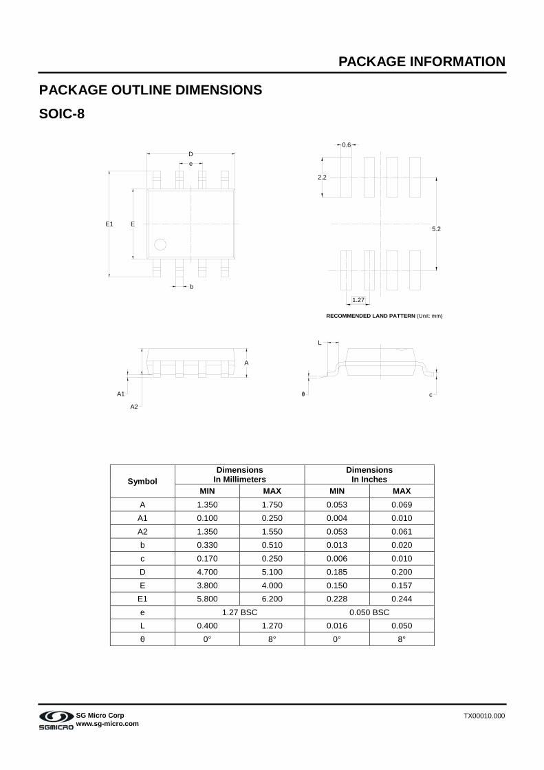
PACKAGE OUTLINE DIMENSIONS SOIC-8
Symbol Dimensions
In Millimeters Dimensions
In Inches MIN MAX MIN MAX
A 1.350 1.750 0.053 0.069 A1 0.100 0.250 0.004 0.010 A2 1.350 1.550 0.053 0.061 b 0.330 0.510 0.013 0.020 c 0.170 0.250 0.006 0.010 D 4.700 5.100 0.185 0.200 E 3.800 4.000 0.150 0.157
E1 5.800 6.200 0.228 0.244 e 1.27 BSC 0.050 BSC L 0.400 1.270 0.016 0.050 θ 0° 8° 0° 8°
D
EE1
e
b
A
A2
A1 c
L
θ
1.27
0.6
2.2
5.2
RECOMMENDED LAND PATTERN (Unit: mm)
PACKAGE INFORMATION
TX00014.000 SG Micro Corp www.sg-micro.com
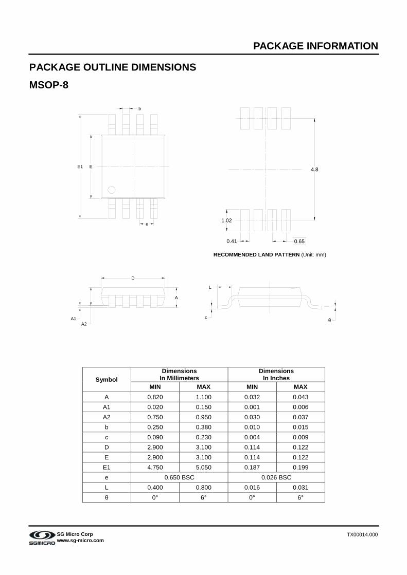
PACKAGE OUTLINE DIMENSIONS MSOP-8
Symbol Dimensions
In Millimeters Dimensions
In Inches MIN MAX MIN MAX
A 0.820 1.100 0.032 0.043 A1 0.020 0.150 0.001 0.006 A2 0.750 0.950 0.030 0.037 b 0.250 0.380 0.010 0.015 c 0.090 0.230 0.004 0.009 D 2.900 3.100 0.114 0.122 E 2.900 3.100 0.114 0.122
E1 4.750 5.050 0.187 0.199 e 0.650 BSC 0.026 BSC L 0.400 0.800 0.016 0.031 θ 0° 6° 0° 6°
E1 E
e
D
A1
L
c
A
A2 θ
b
RECOMMENDED LAND PATTERN (Unit: mm)
1.02
0.41 0.65
4.8
PACKAGE INFORMATION
TX00018.000 SG Micro Corp www.sg-micro.com
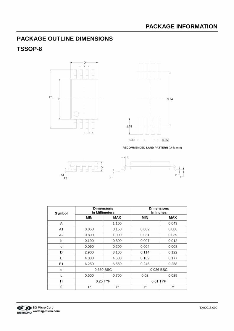
PACKAGE OUTLINE DIMENSIONS TSSOP-8
Symbol Dimensions
In Millimeters Dimensions
In Inches MIN MAX MIN MAX
A 1.100 0.043 A1 0.050 0.150 0.002 0.006 A2 0.800 1.000 0.031 0.039 b 0.190 0.300 0.007 0.012 c 0.090 0.200 0.004 0.008 D 2.900 3.100 0.114 0.122 E 4.300 4.500 0.169 0.177
E1 6.250 6.550 0.246 0.258 e 0.650 BSC 0.026 BSC L 0.500 0.700 0.02 0.028 H 0.25 TYP 0.01 TYP θ 1° 7° 1° 7°
EE1
De
b
A
θ
L
cHA1A2
0.65
1.78
0.42
5.94
RECOMMENDED LAND PATTERN (Unit: mm)
PACKAGE INFORMATION
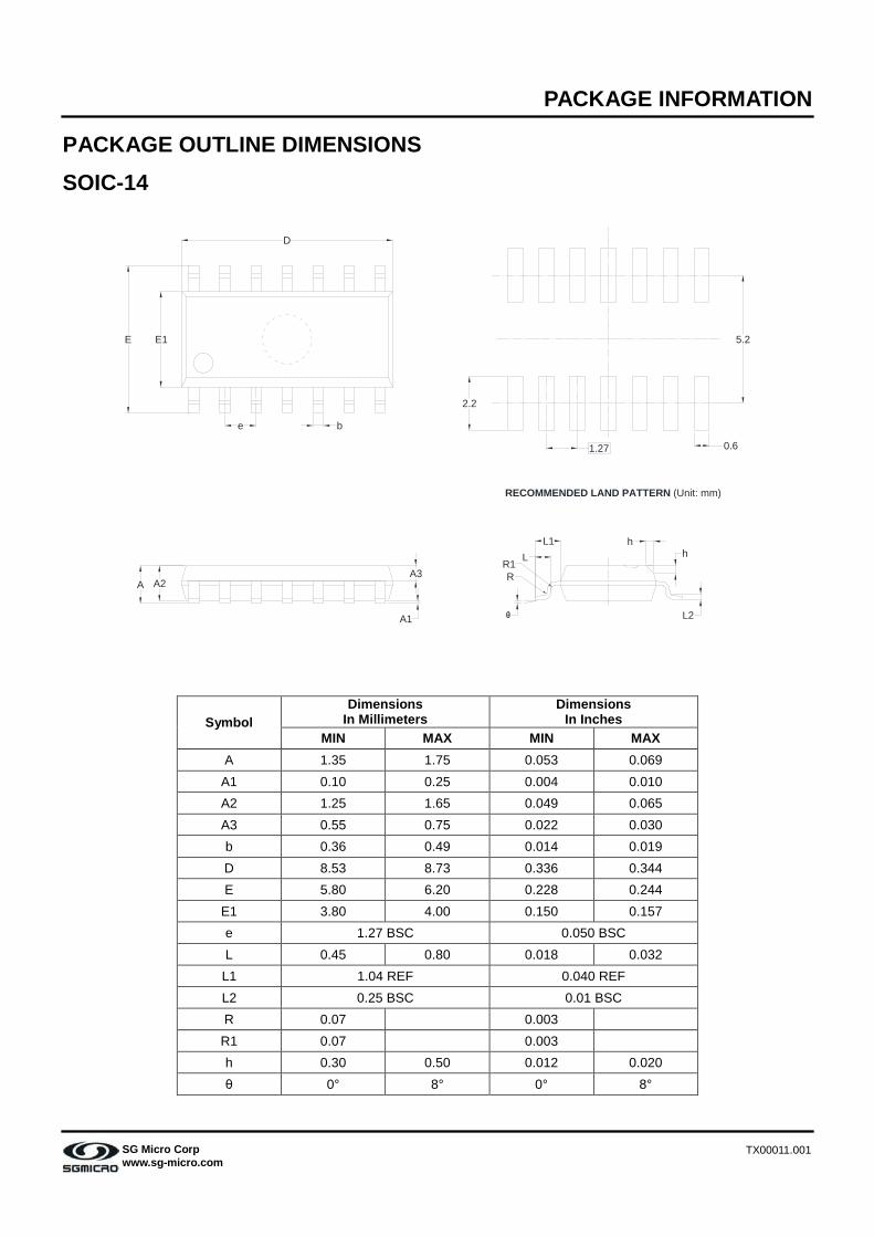
TX00011.001 SG Micro Corp www.sg-micro.com
PACKAGE OUTLINE DIMENSIONS SOIC-14
Symbol Dimensions
In Millimeters Dimensions
In Inches MIN MAX MIN MAX
A 1.35 1.75 0.053 0.069 A1 0.10 0.25 0.004 0.010 A2 1.25 1.65 0.049 0.065 A3 0.55 0.75 0.022 0.030 b 0.36 0.49 0.014 0.019 D 8.53 8.73 0.336 0.344 E 5.80 6.20 0.228 0.244
E1 3.80 4.00 0.150 0.157 e 1.27 BSC 0.050 BSC L 0.45 0.80 0.018 0.032 L1 1.04 REF 0.040 REF L2 0.25 BSC 0.01 BSC R 0.07 0.003
R1 0.07 0.003 h 0.30 0.50 0.012 0.020 θ 0° 8° 0° 8°
RECOMMENDED LAND PATTERN (Unit: mm)
D
E1E
θ
L1
L2
A3A A2
5.2
1.27 0.6
2.2
e b
A1
Lh
h
RR1
PACKAGE INFORMATION
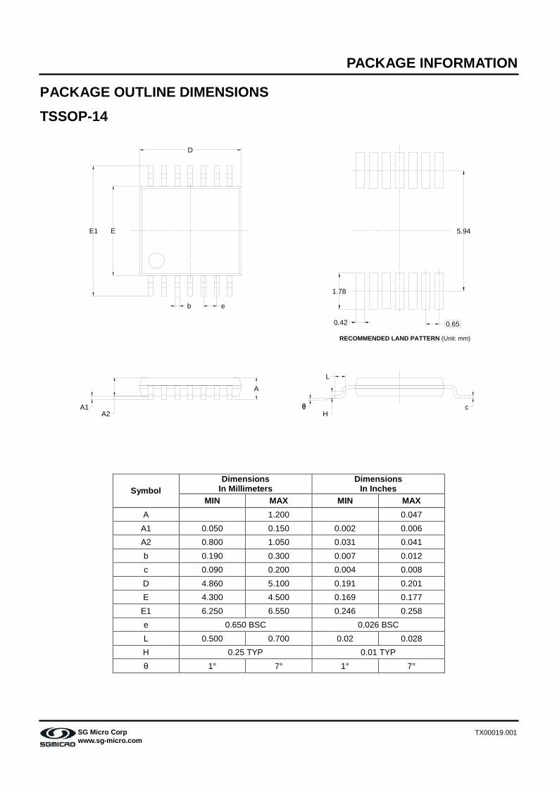
TX00019.001 SG Micro Corp www.sg-micro.com
PACKAGE OUTLINE DIMENSIONS TSSOP-14
Symbol Dimensions
In Millimeters Dimensions
In Inches MIN MAX MIN MAX
A 1.200 0.047 A1 0.050 0.150 0.002 0.006 A2 0.800 1.050 0.031 0.041 b 0.190 0.300 0.007 0.012 c 0.090 0.200 0.004 0.008 D 4.860 5.100 0.191 0.201 E 4.300 4.500 0.169 0.177
E1 6.250 6.550 0.246 0.258 e 0.650 BSC 0.026 BSC L 0.500 0.700 0.02 0.028 H 0.25 TYP 0.01 TYP θ 1° 7° 1° 7°
EE1
D
b
A
A1A2
θ
L
cH
e
RECOMMENDED LAND PATTERN (Unit: mm)
5.94
0.42
1.78
0.65
PACKAGE INFORMATION
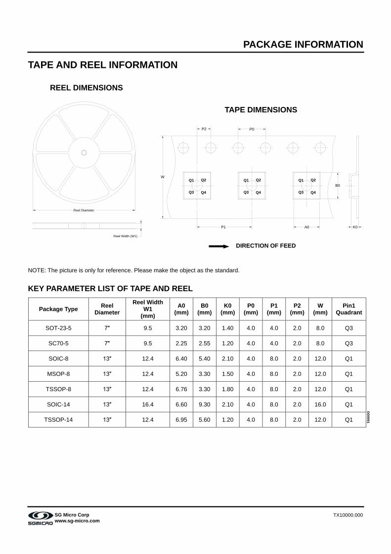
TX10000.000 SG Micro Corp www.sg-micro.com
TAPE AND REEL INFORMATION NOTE: The picture is only for reference. Please make the object as the standard.
KEY PARAMETER LIST OF TAPE AND REEL
Package Type Reel Diameter
Reel Width W1
(mm) A0
(mm) B0
(mm) K0
(mm) P0
(mm) P1
(mm) P2
(mm) W
(mm) Pin1
Quadrant
DD
0001
SOT-23-5 7″ 9.5 3.20 3.20 1.40 4.0 4.0 2.0 8.0 Q3
SC70-5 7″ 9.5 2.25 2.55 1.20 4.0 4.0 2.0 8.0 Q3
SOIC-8 13″ 12.4 6.40 5.40 2.10 4.0 8.0 2.0 12.0 Q1
MSOP-8 13″ 12.4 5.20 3.30 1.50 4.0 8.0 2.0 12.0 Q1
TSSOP-8 13″ 12.4 6.76 3.30 1.80 4.0 8.0 2.0 12.0 Q1
SOIC-14 13″ 16.4 6.60 9.30 2.10 4.0 8.0 2.0 16.0 Q1
TSSOP-14 13″ 12.4 6.95 5.60 1.20 4.0 8.0 2.0 12.0 Q1
Reel Width (W1)
Reel Diameter
REEL DIMENSIONS
TAPE DIMENSIONS
DIRECTION OF FEED
P2 P0
W
P1 A0 K0
B0Q1 Q2
Q4Q3 Q3 Q4
Q2Q1
Q3 Q4
Q2Q1
PACKAGE INFORMATION
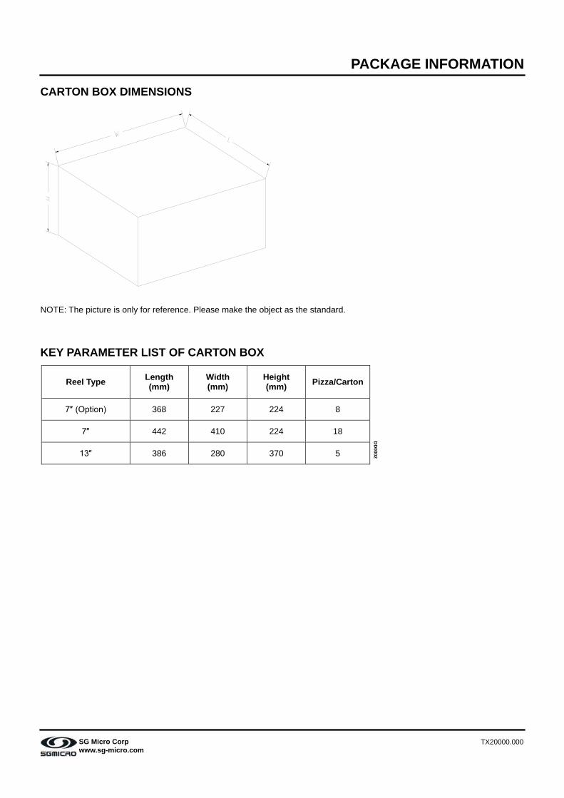
TX20000.000 SG Micro Corp www.sg-micro.com
CARTON BOX DIMENSIONS
NOTE: The picture is only for reference. Please make the object as the standard.
KEY PARAMETER LIST OF CARTON BOX
Reel Type Length (mm)
Width (mm)
Height (mm) Pizza/Carton
DD
0002
7″ (Option) 368 227 224 8
7″ 442 410 224 18
13″ 386 280 370 5