
Wide Dissemination of Pseudomonas aeruginosa Producing β ...
TCAD analysis of wide-spectrum waveguides inhigh-voltage SOI-CMOS
Satadal Dutta1, Luis Orbe2, and Jurriaan Schmitz1.1 MESA+ Institute for Nanotechnology, University of Twente, 2 Phoenix B.V., Enschede, The Netherlands.
Abstract—A TCAD based analysis is presented on the trans-mission efficiency η of silicon-on-insulator (SOI) and siliconnitride slab waveguides in a high-voltage standard SOI-CMOStechnology, for the spectral range of 480 nm - 1300 nm, andisotropic optical excitation via monolithic Si-based LEDs. Theeffects of geometry, wavelength and galvanic isolation on η arereported.
The integration of photonic functionality in CMOSis promising for high-speed data communication, andopto-electronic system-on-chip applications. For mostcontemporary photonic and/or opto-electronic integratedcircuits [1]–[5], CMOS technology is commonly extendedwith a dedicated waveguide (WG) layer having a low materialabsorption coefficient (α) and a high refractive index (n)for photonic functionalities [1]. Some industrial CMOStechnologies, however, offer built-in thin films suitable asWGs, the most common being the silicon (Si) layer insilicon-on-insulator (SOI) technology [1], [5]–[7]. Recently, amonolithic optocoupler was realized in standard high-voltageSOI CMOS [6], which not only includes an SOI layeras a WG for infrared (IR) light, but also a thin siliconnitride (Si3N4) film laid atop the active Si surface, which is apotential WG for visible and IR light [7]–[12]. In addition, theoptocoupler comprises an Si LED that exhibits wide-spectrum(400 nm < λ < 1300 nm ) and isotropic electroluminescence(EL). An Si photodiode (PD) detects light laterally. Suchfeatures of the LED, combined with the inherent off-axisalignment of the WGs w.r.t. the LED and the PD, makes theoptical transmission efficiency η(λ ) rather difficult to analyzeby means other than numerical TCAD simulation.
In this work we first show, using raytracing simulations inSentaurus, the built-in WG conditions for SOI and Si3N4 corelayers with SiO2 cladding, leading to anisotropic transmission.Secondly, via hybrid-mode EM wave simulations, we showhow η(λ ) is affected by geometry; namely SOI and/or nitridethickness tSOI/Si3N4, link length L, and galvanic isolation in atypical SOI-based optocoupler, with on-chip isotropic opticalexcitation.
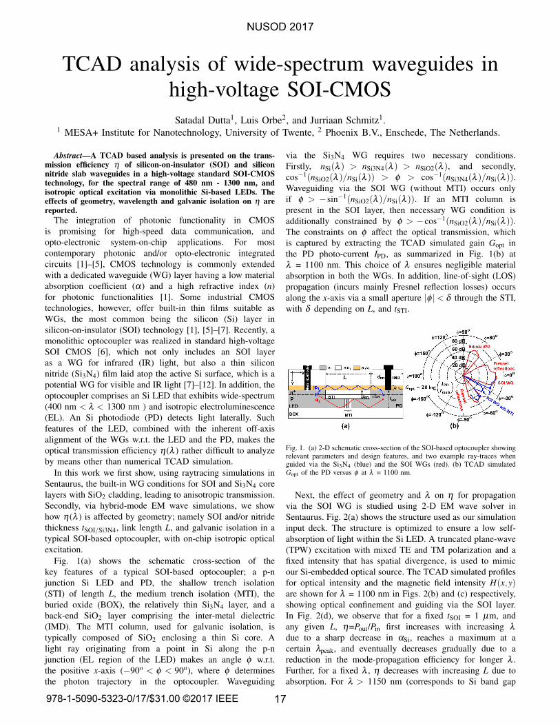
Fig. 1(a) shows the schematic cross-section of thekey features of a typical SOI-based optocoupler; a p-njunction Si LED and PD, the shallow trench isolation(STI) of length L, the medium trench isolation (MTI), theburied oxide (BOX), the relatively thin Si3N4 layer, and aback-end SiO2 layer comprising the inter-metal dielectric(IMD). The MTI column, used for galvanic isolation, istypically composed of SiO2 enclosing a thin Si core. Alight ray originating from a point in Si along the p-njunction (EL region of the LED) makes an angle φ w.r.t.the positive x-axis (−90o < φ < 90o), where φ determinesthe photon trajectory in the optocoupler. Waveguiding
via the Si3N4 WG requires two necessary conditions.Firstly, nSi(λ ) > nSi3N4(λ ) > nSiO2(λ ), and secondly,cos−1(nSiO2(λ )/nSi(λ )) > φ > cos−1(nSi3N4(λ )/nSi(λ )).Waveguiding via the SOI WG (without MTI) occurs onlyif φ > −sin−1(nSiO2(λ )/nSi(λ )). If an MTI column ispresent in the SOI layer, then necessary WG condition isadditionally constrained by φ > −cos−1(nSiO2(λ )/nSi(λ )).The constraints on φ affect the optical transmission, whichis captured by extracting the TCAD simulated gain Gopt inthe PD photo-current IPD, as summarized in Fig. 1(b) atλ = 1100 nm. This choice of λ ensures negligible materialabsorption in both the WGs. In addition, line-of-sight (LOS)propagation (incurs mainly Fresnel reflection losses) occursalong the x-axis via a small aperture |φ |< δ through the STI,with δ depending on L, and tSTI.
Fig. 1. (a) 2-D schematic cross-section of the SOI-based optocoupler showingrelevant parameters and design features, and two example ray-traces whenguided via the Si3N4 (blue) and the SOI WGs (red). (b) TCAD simulatedGopt of the PD versus φ at λ = 1100 nm.
Next, the effect of geometry and λ on η for propagationvia the SOI WG is studied using 2-D EM wave solver inSentaurus. Fig. 2(a) shows the structure used as our simulationinput deck. The structure is optimized to ensure a low self-absorption of light within the Si LED. A truncated plane-wave(TPW) excitation with mixed TE and TM polarization and afixed intensity that has spatial divergence, is used to mimicour Si-embedded optical source. The TCAD simulated profilesfor optical intensity and the magnetic field intensity H(x,y)are shown for λ = 1100 nm in Figs. 2(b) and (c) respectively,showing optical confinement and guiding via the SOI layer.In Fig. 2(d), we observe that for a fixed tSOI = 1 µm, andany given L, η=Pout/Pin first increases with increasing λ
due to a sharp decrease in αSi, reaches a maximum at acertain λpeak, and eventually decreases gradually due to areduction in the mode-propagation efficiency for longer λ .Further, for a fixed λ , η decreases with increasing L due toabsorption. For λ > 1150 nm (corresponds to Si band gap
NUSOD 2017
17978-1-5090-5323-0/17/$31.00 ©2017 IEEE
of 1.12 eV), η is significantly less sensitive to L, due tonegligible absorption at such long λ . In Fig. 2(e), we observethat for a fixed L, η(λ ) increases as tSOI is increased from 1µm to 2 µm, due to increased mode-propagation efficiency.This also explains the observation that η(λ ) increases tillλ = 1300 nm for tSOI = 2 µm; λpeak being shifted beyond1300 nm. Further, the presence of the MTI, leads to a fixedadditional 20 % reduction in η for any L and tSOI, caused byFresnel reflections at the Si-SiO2 interfaces. The ripples inη(λ ) are likely caused by inter-modal interference.
Fig. 2. (a) The SOI WG: The time-averaged and y-integrated input (Pin) andoutput (Pout) optical powers are evaluated at x=–0.5 L and x=0.5 L respectively.Convolutional Perfectly Matched Layer (CPML) boundary conditions areassumed in both x and y directions, and tSTI=0.4 µm. (b) Optical intensityprofile and (c) Magnetic field intensity profile at λ=1100 nm. (d) and (e)Simulated η for indicated values of L and tSOI.
Fig. 3. (a) The Si3N4 WG: Time-averaged and y-integrated input (Pin) andoutput (Pout) optical powers are evaluated at x=–0.5 L and x=0.5 L respectively.CPML boundary conditions are assumed for both x and y axes. (b) Opticalintensity profile and (c) Magnetic field intensity profile at λ=600 nm. (d) and(e) Simulated η for indicated values of L and tSi3N4.
Fig. 3(a) shows the optimized structure used to simulate theSi3N4 WG. The TPW excitation (constrained by the solver to
be placed in vacuum) is given an initial orientation φ ≈ 62o.This mimics our Si-based optical source without violatingthe aforesaid necessary conditions for waveguiding. Figs. 3(b)and (c) show the intensity profile and H(x,y) respectively atλ = 600 nm, showing out-of-plane guiding. Light is coupledin from the Si LED into Si3N4, and is coupled out from Si3N4to the Si PD. The Si3N4 core is optically much thinner thanthe SOI core. In Fig. 3(d), we observe that for a fixed tSi3N4and L, η falls sharply with increasing λ . A slight increasein η is observed for λ ≥ 1100 nm, which can be explainedby an increased edge-coupling to the underlying SOI layer,thereby augmenting Pout and hence η for longer λ . Further,η(λ ) shows a much smaller L-dependence (attenuation) thanobserved in the SOI case, due to the much lower αSi3N4. Inreal structures, however, a higher attenuation is expected [6]because of roughness in the core-cladding interface (ignoredin our simulation). For any L, as tSi3N4 is doubled from 0.2 µmto 0.4 µm, a ∼ 15 % increase in η(λ ) is observed dueto increased mode-propagation efficiency; the increase beingmore pronounced at longer λ .
The η(λ ) for all the optical paths can be combined toobtain the cumulative weighted η(λ ) over the entire range ofφ to mimic an isotropic optical source, as shown in Fig. 4(a).Transmission is dominated by the Si3N4 WG for λ <700 nm,and by the SOI WG for λ >700 nm. Our TCAD analysisprovides some key guidelines for designers to optimize opticalpropagation in standard SOI CMOS technology, involvingembedded wide-spectrum and isotropic light sources, as high-lighted in Fig. 4(b).
Fig. 4. (a) φ -weighted cumulative transmission efficiencies for indicatedgeometrical parameters assuming isotropic EL combining the three opticalpaths: Si3N4 WG, SOI WG, and LOS. The weights wi(λ ) are calculatedusing the allowed range of φ for each path, such that Σwi(λ ) = 1. The meanspectral efficiency < η > is indicated for each case. (b) Summary of the keytake-away messages of our work and its potential scope of application.
REFERENCES
[1] C. Sun et al., Nature, vol. 528, pp. 534-538, 2015.[2] M. du Plessis et al., IEEE J. Sel. Topics Quantum Electron., vol. 8, no.
6, pp. 1412-1419, 2002.[3] B. Huang et al., Opt. Commun., vol. 284, no. 16-17, pp. 3924-3927, 2011.[4] A. Khanmohammadi et al., Proc. 45th ESSDERC, pp. 138-141, 2015.[5] N. Rouger et al., Proc. 28th ISPSD, pp. 427-430, 2016.[6] S. Dutta et al., Opt. Express, vol. 25, no.4, pp. 5440-5456, 2017.[7] R. Baets et al., in proc. OFC 2016, p. Th3J.1.[8] A.Z. Subramanian et al., IEEE Photonics J., vol. 5, no. 6, 2013.[9] M. Melchiorri et al., Appl. Phys. Lett., vol. 86, 121111, 2005.[10] H. Yamada, Piers Online, vol. 6, no. 2, 2010.[11] G. Li et al, Opt. Express, vol. 20, no. 11, pp. 12035-12039, 2012.[12] F. Grillot et al., J. Lightwave Tech., vol. 24, no. 2, 2006.
NUSOD 2017
18


![Quasars, Pulsars, Gamma- Ray Bursts! Oh, my!heyl/ASTR304_2003W/Week1.pdf · 2004. 1. 9. · Quasars - Active Galaxies]The nuclear activity of galaxies spans a wide spectrum ranging](https://static.fdocument.org/doc/165x107/6123ca19300cba04710388ff/quasars-pulsars-gamma-ray-bursts-oh-my-heylastr3042003wweek1pdf-2004.jpg)