RADIO ENGINEERING III - gimmenotes
84
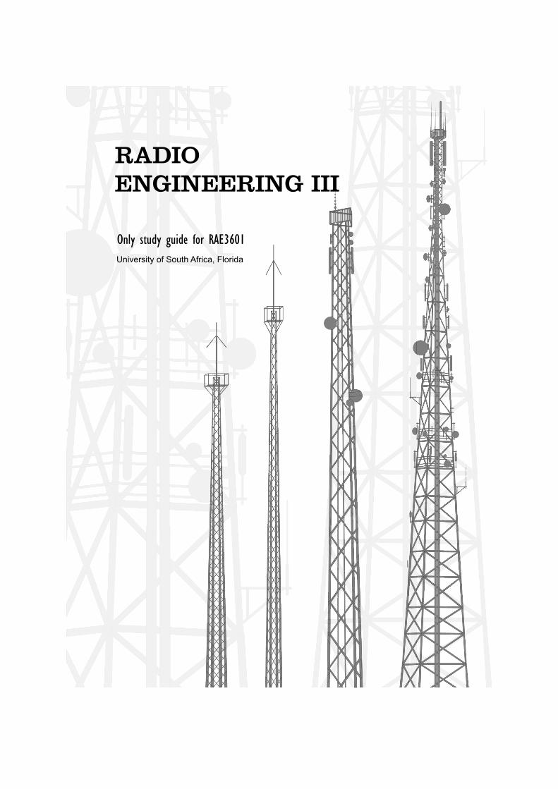
RADIO ENGINEERING III Only study guide for RAE3601
Transcript of RADIO ENGINEERING III - gimmenotes
RADIO ENGINEERING III
Only study guide for RAE3601
© 2018 University of South Africa
All rights reserved
Printed and published by the University of South Africa Muckleneuk, Pretoria
RAE3601/1/2019–2022
70675953
InDesign Florida
PR_Tour_Style
. . . . . . . . . . .R AE 36 01/1iii
CONTENTS
Page
Study unit 1: INTRODUCTION TO COMMUNICATION SYSTEMS 11.1 Learning outcomes 11.2 Introduction 11.3 LC circuits 21.4 Tuned small-signal amplifiers, mixers and active filters 21.4.1 Hybrid-π equivalent circuit for the BJT 21.4.2 Tuned radio frequency (RF) amplifiers 41.4.3 Stability and neutralisation 51.4.4 The common-emitter amplifier 71.4.5 The common-base amplifier 71.4.6 Cascade amplifier 81.4.7 Mixer circuits 91.5 LC oscillators 121.5.1 Hartley oscillator 141.5.2 Colpitts oscillator 141.5.3 Clapp oscillator 151.5.4 Crystal oscillator 161.6 Questions 17
Study unit 2: NOISE 182.1 Learning outcomes 182.2 Introduction to noise 182.2.1 External noise 182.2.2 Internal noise 18
Study unit 3: AMPLITUDE MODULATION RECEIVERS 203.1 Learning outcomes 203.2 Introduction 203.3 Superheterodyne receivers 203.4 Tuning range 223.5 Tracking 223.6 Image rejection 233.7 Double conversion 243.8 Spurious responses 243.9 Automatic gain control 243.10 Electronically tuned receivers 253.11 Questions 27
Study unit 4: AMPLITUDE MODULATION TRANSMITTERS 284.1 Learning outcomes 284.2 Introduction 284.3 Amplitude modulator circuits 294.4 Amplitude demodulator circuits 304.5 Amplitude modulated (AM) transmitters 30
CO N T EN T S
. . . . . . . . . . .iv
4.6 Noise in AM systems 314.7 Questions 32
Study unit 5: THE SINGLE SIDEBAND (SSB) 335.1 Learning outcomes 335.2 Single-sideband principles 335.3 Balanced modulators 345.4 Questions 35
Study unit 6: FREQUENCY MODULATION TRANSMITTERS AND RECEIVERS 366.1 Learning outcomes 366.2 Frequency modulation 366.3 Angle modulator circuits 386.4 FM transmission 396.5 Angle modulator detectors (receivers) 416.6 Amplitude limiters 426.7 Questions 43
Study unit 7: INTRODUCTION TO DIGITAL COMMUNICATION 447.1 Learning outcomes 447.2 Digital communications 447.3 Pulse amplitude modulation 477.4 Quantisation 487.5 Synchronous vs asynchronous systems 497.6 Bit errors 497.7 Questions 50
Study unit 8: TRANSMISSION LINES AND CABLES 518.1 Learning outcomes 518.2 Types of transmission lines 518.2.1 Balanced lines 518.2.2 Unbalanced lines 528.3 Transmission line characteristics for a two-wire system 528.4 Transmission lines characteristics for a co-axial system 558.5 Voltage propagation in transmission lines 568.6 Non-resonant and resonant lines 568.7 AC vs DC 588.8 Standing wave ratio (SWR) 588.9 Impedance matching 608.9.1 Quarter wavelength matching transformer 608.9.2 Single-stub tuning 618.10 Transmission line applications 618.10.1 Discrete circuit simulation 618.10.2 Baluns 618.10.3 Filters 628.10.4 Slotted lines 628.10.5 Time-domain reflectometry 628.11 Questions 62
Study unit 9: RADIO WAVE PROPAGATION 649.1 Learning outcomes 649.2 Electromagnetic waves 64
Co ntent s
. . . . . . . . . . .R AE 36 01/1v
. . . . . . . . . . .R AE 36 01/1v
9.2.1 Electrical to electromagnetic conversion 649.2.2 Electromagnetic waves 649.2.3 Waves not in free space 669.3 Ground-space-sky-wave and satellite propagation 669.4 Questions 68
Study unit 10: ANTENNA THEORY 6910.1 Learning outcomes 6910.2 Half-wave dipole antenna 6910.3 Antenna gain 7110.4 Radiation patterns 7210.5 Antenna arrays 7410.6 Questions 76
. . . . . . . . . . .vi
STUDY UNIT 0
ABOUT THIS MODULE
0.1 WELCOME
Welcome to Radio Engineering III (RAE3601), a module offered by Unisa’s Department of Electrical and Mining Engineering. The lecturer for this module is Dr M Sumbwanyambe. This module looks at different aspects of radio engineering. There is a recommended textbook for this module – please refer to it at all times. The textbook must be used with the other resources that are available on myUnisa. Please make sure you go through the Additional Resources section of myUnisa.
0.2 PURPOSE OF THE MODULE
Radio engineering, also known as radio frequency engineering, is a study of different kinds of devices that emit and receive radio waves. It is incorporated into almost anything that sends and receives signals such as mobile phones, radios, Wi-Fi and two-way radios. These devices are all part of the broader wireless network. In South Africa, different institutions, such as SENTECH, SABC, MTN and Cell C, all use radio engineering to transport signals from senders to receivers. A basic knowledge of radio engineering is essential for students who are studying electrical engineering.
This module aims to provide you with the basic skills required to analyse and design radio engineering systems. The following topics are discussed in this study guide:
• Introduction to communication systems • Noise • Amplitude modulation receivers • Amplitude modulation transmitters • The single sideband (SSB) • Frequency modulation transmitters and receivers • Introduction to digital communication • Transmission lines and cables • Radio wave propagation • Antenna theory
S T UDY UN I T 0 : Ab out this m o dul e
. . . . . . . . . . .R AE 36 01/1vii
0.3 LEARNING RESOURCES
0.3.1 Prescribed textbook
The following textbook is prescribed for this module:
Beasley, JS & Miller, GM. 2014. Modern electronic communication, 9th edition. Harlow: Pearson Education Limited.
This textbook is your main source of information, therefore you need to buy a copy. Without access to the textbook you will not be able to complete the module successfully.
0.3.2 Additional learning resources
In addition to the textbook, I provide you with several other resources to help you on your journey through radio engineering. Most of these resources can be found under Additional Resources on the myUnisa module site for RAE3601. I also strongly recommend that you consult another book that may be help to broaden your understanding of radio engineering. This book is not prescribed, but it is a very useful resource:
Frenzel, LE. 2016. Principles of electronic communication systems, 4th edition. New York: McGraw-Hill.
0.3.3 Study guide
The purpose of this study guide is to guide you through the prescribed textbook for RAE3601.
• The study guide is divided into nine study units. Each study unit starts with an introduction and a discussion of the objectives of the study unit in relation to the prescribed book. Pay particular attention to the fact that the study guide will only guide you on how to use the textbook and should not be viewed or used as the prescribed book for this module.
• The discussion of each chapter of the prescribed book starts with an introduction, followed by the main objectives of that particular chapter.
• Please note that you must study each chapter and every section of the prescribed book.
• I have included worked examples from the prescribed textbook and activities. Please study them and make sure that you understand them.
• I have supplied a number of problems. Please complete these in order to test yourself.
0.4 MODULE STRUCTURE
This module on Radio Engineering is divided into the following study units:
Study unit 1: Introduction to communication systems
Study unit 2: Noise
Study unit 3: Amplitude modulation receivers
. . . . . . . . . . .viii
Study unit 4: Amplitude modulation transmitters
Study unit 5: The single sideband (SSB)
Study unit 6: Frequency modulation transmitters and receivers
Study unit 7: Introduction to digital communications
Study unit 8: Transmission lines and cables
Study unit 9: Radio wave propagation
Study unit 10: Antenna theory
0.5 LECTURER’S CONTACT DETAILS
My contact details are as follows:
Dr M Sumbwanyambe
Telephone number: 011 471 3378
E-mail: [email protected]
. . . . . . . . . . .R AE 36 01/11
1S T U D Y U N I T 1
1INTRODUCTION TO COMMUNICATION SYSTEMS
1.1 LEARNING OUTCOMESOnce you have completed this study unit, you should be able to do the following:
• Identify and differentiate between the blocks in the communication system. • Interpret the function of each block in the communication system. • Explain and calculate the use of the dB in the communication system.
1.2 INTRODUCTIONThe study of communication systems is important to our everyday life. Basically, the main purpose of communication systems is to allow for the transfer of signals, which may be data or voice signals, from the sender to the receiver through a medium. This medium can be wireless or wired. Wired media include copper cables, fibre optic cables, coaxial cables and even power lines. Wireless media are used for cellular, Wi-Fi and WiMAX communication, among other wireless technologies.
The communication systems are composed of three basic components, namely the sender component, the medium component and the receiver component. The sender (transmitter) side is composed of elements that allow the capturing of a human voice and converted it into high-frequency signals that can then be transmitted over the medium. This is usually done through a transducer such as a microphone. A transducer is a device that converts signal energy from one form to another. It then passes through a modulator, an amplifier and then the communication medium. At the receiver side, the signal is again passed through an amplifier, a demodulator and an output transducer (normally a speaker).
Turn to figure 1 in the textbook (Beasley & Miller, 2014:6). Study chapter 1 of the textbook (Beasley & Miller, 2014) and pay particular attention to pages 4 to 7. Study the block diagram of a communication system (figure 1) carefully. You must be able to describe all the stages and the functions of all the components of the communication system.
. . . . . . . . . . .2
In any telecommunication system, decibels (dBs) are used to specify measured and calculated values in noise analysis, audio systems, microwave system gain calculations, satellite system link-budget analysis, antenna power gain and light-budget calculations. In each case, the dB value is calculated with respect to a standard or specified reference. The decibel is usually the ratio of the calculated power (P2) to a reference power (P1). It is calculated as follows:
By using the power relationship of voltage and resistance, the dB can also be expressed as the factor of voltage.
Work through examples 1 and 2 of the textbook (Beasley & Miller, 2014:8–9).
You must be able to use table 2 (Beasley & Miller, 2014:11), the conversion table for common dBm values, to convert from dBm to dBw given different equivalent voltages and resistance. Work through example 3 (Beasley & Miller, 2014:10).
1.3 LC CIRCUITSLC circuits are used widely in telecommunications systems, therefore it is prudent for us to introduce them here. You must have a basic understanding of LC circuits to fully appreciate telecommunication systems. LC circuits are circuits that can amplify and/or cut off some of the undesirable signals, such as noise. When designed properly, LC circuits can ensure that a listener will receive a noise-free signal or intelligence. Study page 35 of the textbook (Beasley & Miller, 2014), where these circuits are discussed. Pay particular attention to the terms resonance, bandpass filter, tank circuit and stray capacitance. A tank circuit is any parallel LC circuit that is used in telecommunication systems and is one of the basic BJT circuits that you have studied BJTs in the early stages of your electrical engineering qualification. To refresh your memory, let us return to some of these circuits and how they are applied in telecommunication circuitry.
1.4 TUNED SMALL-SIGNAL AMPLIFIERS, MIXERS AND ACTIVE FILTERS
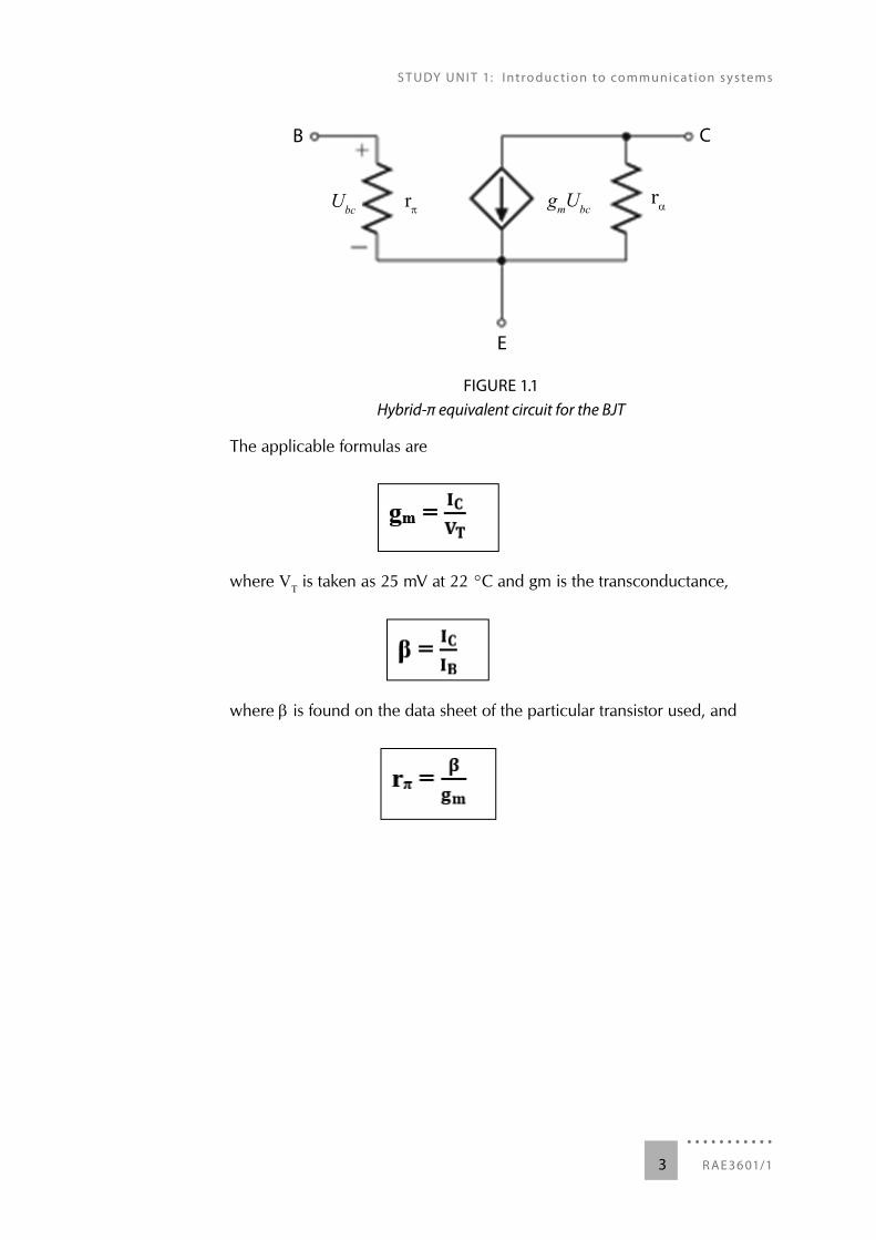
1.4.1 Hybrid-π equivalent circuit for the BJTThis circuit models small-signal behaviour in a transistor (see figure 1.1). It is accurate for low frequencies, but needs to be adapted for higher frequencies by taking into account the capacitance that exists between the electrodes.
S T UDY UN I T 1: Intro du c t io n to co mmunic at io n s ys tems
. . . . . . . . . . .R AE 36 01/13
B
E
C
rαrπUbc gmUbc
FIGURE 1.1Hybrid-π equivalent circuit for the BJT
The applicable formulas are
where VT is taken as 25 mV at 22 °C and gm is the transconductance,
where β is found on the data sheet of the particular transistor used, and
. . . . . . . . . . .4
Question:
For a transistor with the following characteristics, calculate the base current as well as rπ:
IC = 1 mA; VT = 12 V; β = 80
Answer:
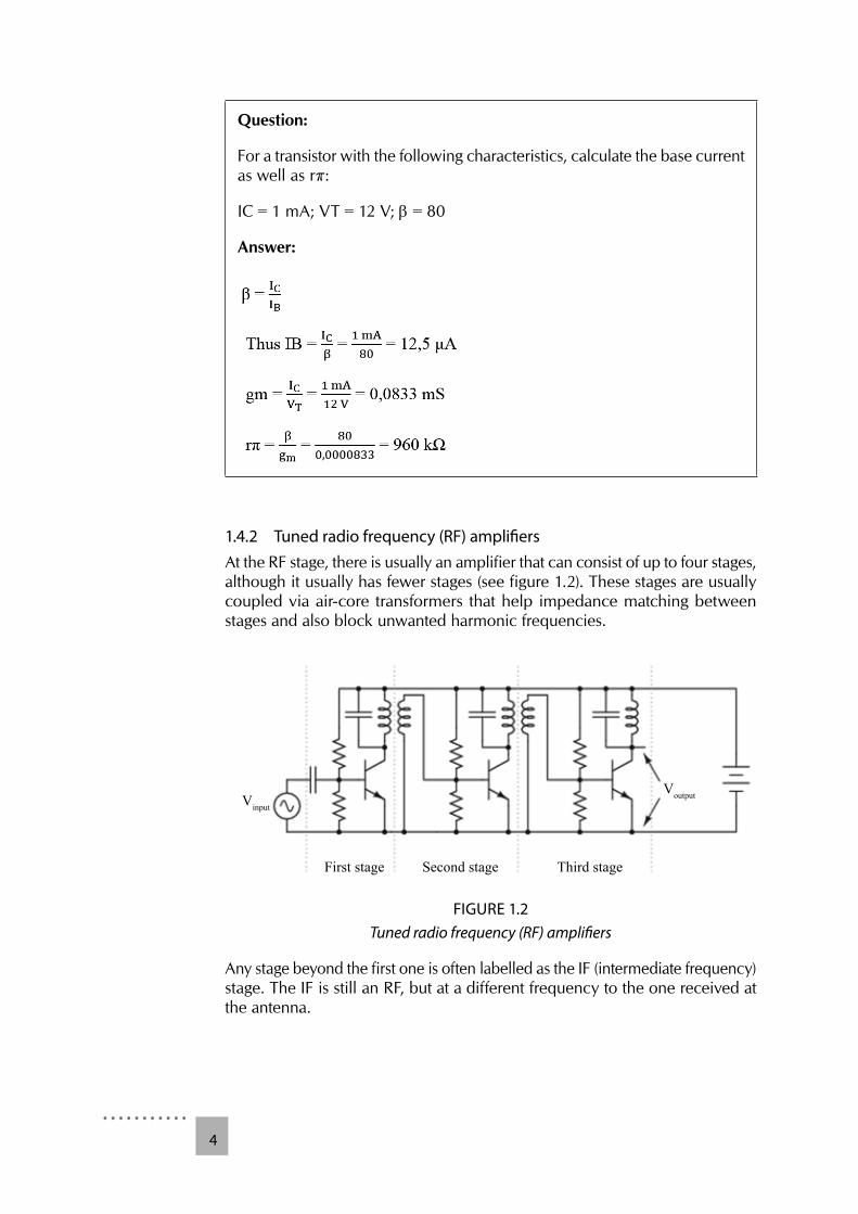
1.4.2 Tuned radio frequency (RF) amplifi ersAt the RF stage, there is usually an amplifier that can consist of up to four stages, although it usually has fewer stages (see figure 1.2). These stages are usually coupled via air-core transformers that help impedance matching between stages and also block unwanted harmonic frequencies.
Vinput
Voutput
First stage Second stage Third stage
FIGURE 1.2Tuned radio frequency (RF) amplifi ers
Any stage beyond the first one is often labelled as the IF (intermediate frequency) stage. The IF is still an RF, but at a different frequency to the one received at the antenna.
S T UDY UN I T 1: Intro du c t io n to co mmunic at io n s ys tems
. . . . . . . . . . .R AE 36 01/15
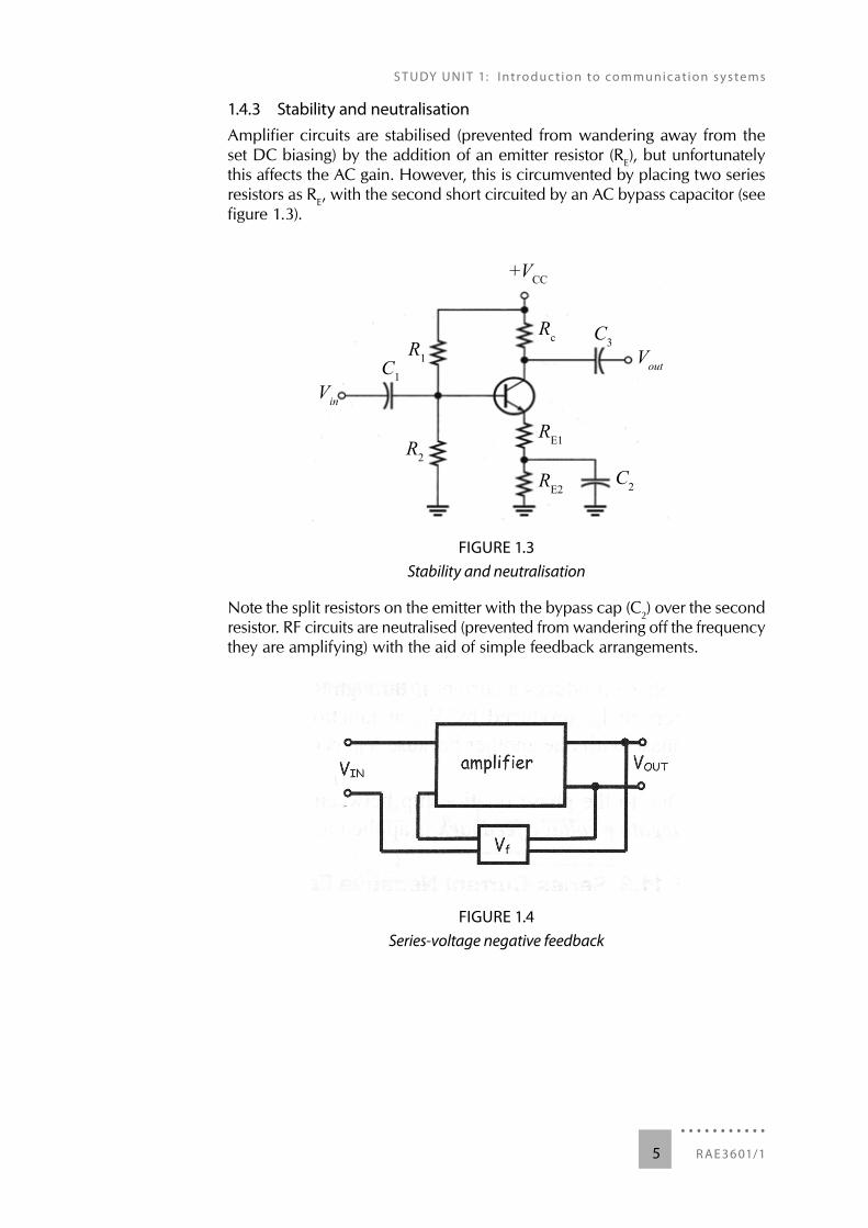
1.4.3 Stability and neutralisationAmplifier circuits are stabilised (prevented from wandering away from the set DC biasing) by the addition of an emitter resistor (RE), but unfortunately this affects the AC gain. However, this is circumvented by placing two series resistors as RE, with the second short circuited by an AC bypass capacitor (see figure 1.3).
Vin
Vout
+VCC
Rc
RE1
RE2
C3
C2
C1
R1
R2
FIGURE 1.3Stability and neutralisation
Note the split resistors on the emitter with the bypass cap (C2) over the second resistor. RF circuits are neutralised (prevented from wandering off the frequency they are amplifying) with the aid of simple feedback arrangements.
FIGURE 1.4Series-voltage negative feedback
. . . . . . . . . . .6
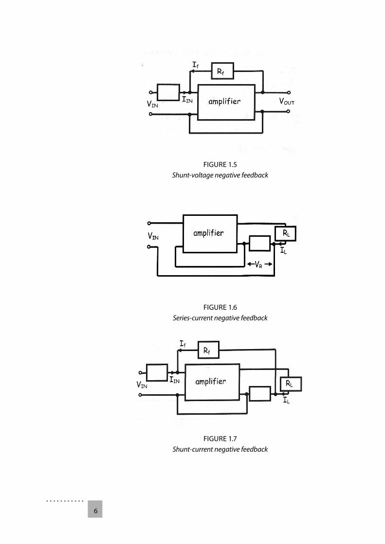
FIGURE 1.5Shunt-voltage negative feedback
FIGURE 1.6Series-current negative feedback
FIGURE 1.7Shunt-current negative feedback
S T UDY UN I T 1: Intro du c t io n to co mmunic at io n s ys tems
. . . . . . . . . . .R AE 36 01/17
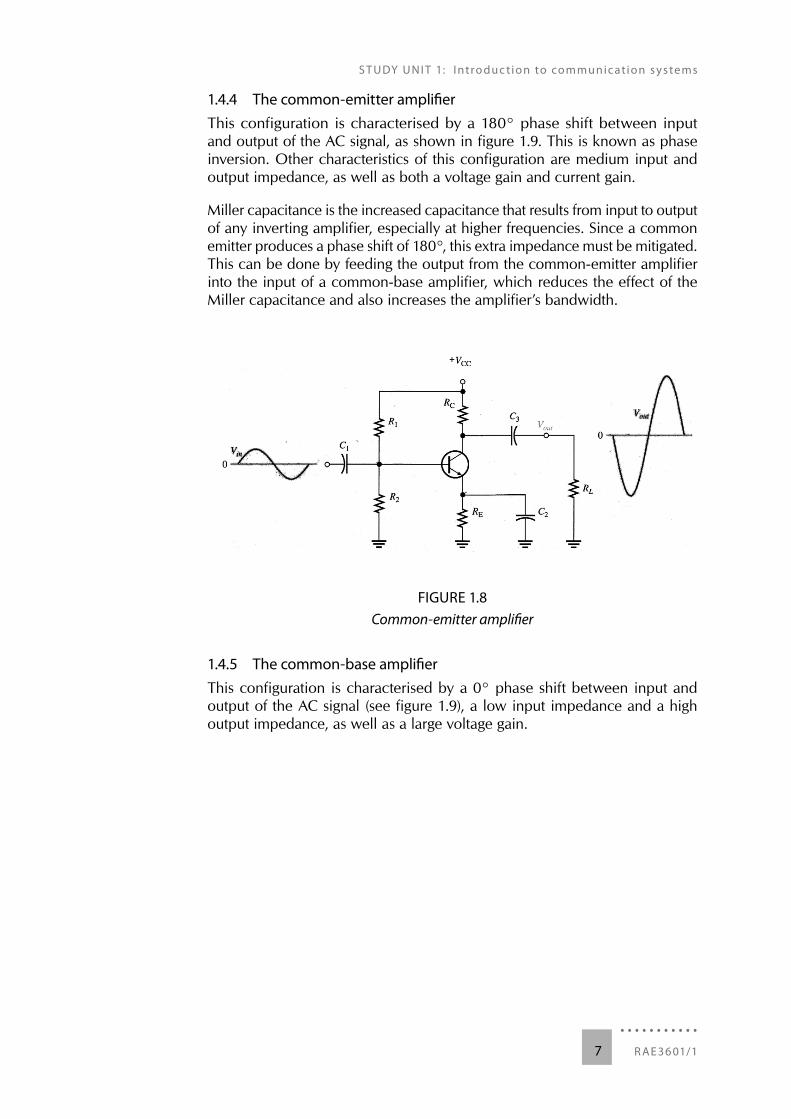
1.4.4 The common-emitter amplifi erThis configuration is characterised by a 180° phase shift between input and output of the AC signal, as shown in figure 1.9. This is known as phase inversion. Other characteristics of this configuration are medium input and output impedance, as well as both a voltage gain and current gain.
Miller capacitance is the increased capacitance that results from input to output of any inverting amplifier, especially at higher frequencies. Since a common emitter produces a phase shift of 180°, this extra impedance must be mitigated. This can be done by feeding the output from the common-emitter amplifier into the input of a common-base amplifier, which reduces the effect of the Miller capacitance and also increases the amplifier’s bandwidth.
FIGURE 1.8Common-emitter amplifi er
1.4.5 The common-base amplifi erThis configuration is characterised by a 0° phase shift between input and output of the AC signal (see figure 1.9), a low input impedance and a high output impedance, as well as a large voltage gain.

. . . . . . . . . . .8
FIGURE 1.9Common-base amplifier
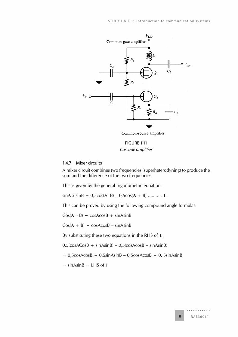
1.4.6 Cascade amplifierAn RF amplifier is formed by joining the output of a common emitter to a common base. It is used to eliminate the Miller effect and to improve the amplifier’s bandwidth. (See figures 1.10 and 1.11.)
FIGURE 1.10Cascade amplifiers are usually built using FETs for common base,
common emitter and cascade amplifiers
S T UDY UN I T 1: Intro du c t io n to co mmunic at io n s ys tems
. . . . . . . . . . .R AE 36 01/19
FIGURE 1.11Cascade amplifier
1.4.7 Mixer circuitsA mixer circuit combines two frequencies (superheterodyning) to produce the sum and the difference of the two frequencies.
This is given by the general trigonometric equation:
sinA x sinB = 0,5cos(A–B) – 0,5cos(A + B) ……….. 1.
This can be proved by using the following compound angle formulas:
Cos(A – B) = cosAcosB + sinAsinB
Cos(A + B) = cosAcosB – sinAsinB
By substituting these two equations in the RHS of 1:
0,5(cosACosB + sinAsinB) – 0,5(cosAcosB – sinAsinB)
= 0,5cosAcosB + 0,5sinAsinB – 0,5cosAcosB + 0, 5sinAsinB
= sinAsinB = LHS of 1
. . . . . . . . . . .10
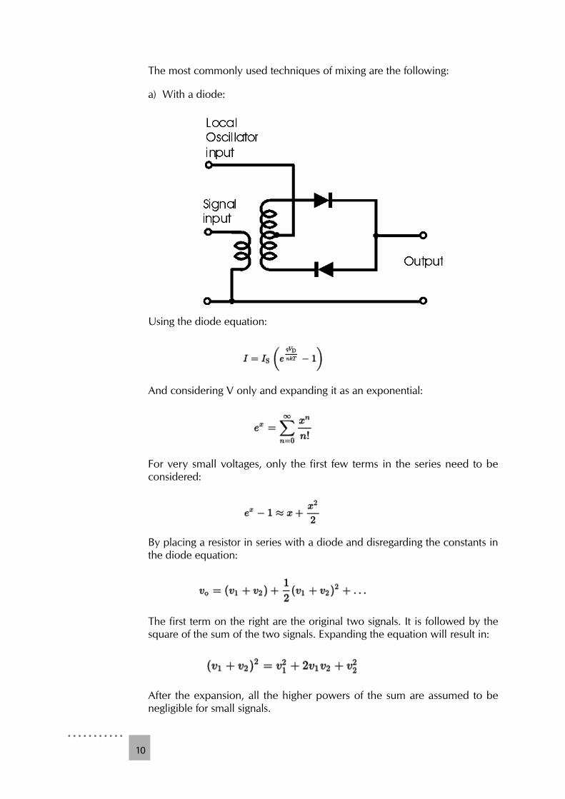
The most commonly used techniques of mixing are the following:
a) With a diode:
Using the diode equation:
And considering V only and expanding it as an exponential:
For very small voltages, only the first few terms in the series need to be considered:
By placing a resistor in series with a diode and disregarding the constants in the diode equation:
The first term on the right are the original two signals. It is followed by the square of the sum of the two signals. Expanding the equation will result in:
After the expansion, all the higher powers of the sum are assumed to be negligible for small signals.
S T UDY UN I T 1: Intro du c t io n to co mmunic at io n s ys tems
. . . . . . . . . . .R AE 36 01/111
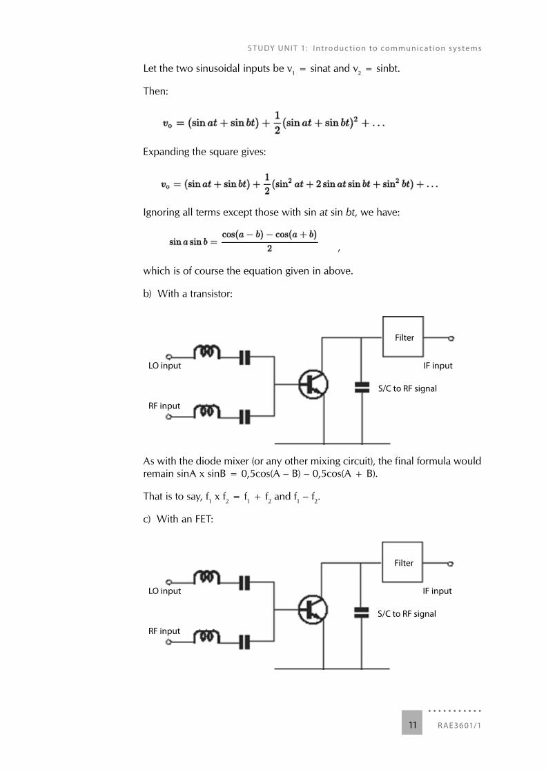
Let the two sinusoidal inputs be v1 = sinat and v2 = sinbt.
Then:
Expanding the square gives:
Ignoring all terms except those with sin at sin bt, we have:
,
which is of course the equation given in above.
b) With a transistor:
LO input IF input
S/C to RF signal
RF input
Filter
As with the diode mixer (or any other mixing circuit), the final formula would remain sinA x sinB = 0,5cos(A – B) – 0,5cos(A + B).
That is to say, f1 x f2 = f1 + f2 and f1 – f2.
c) With an FET:
LO input IF input
S/C to RF signal
RF input
Filter
. . . . . . . . . . .12
1Ac tiv it y
Answer the following questions:
(1) For a transistor with a β of 50, calculate the output resistance if the collector current is 1,2 mA.
(2) Name the characteristics of a common-base amplifier.(3) What is the Miller effect?(4) Briefly explain what a cascade amplifier is and state its purpose.(5) If two sine waves, 105 kHz and 110 kHz, are placed through a mixing
circuit, what will the resultant output frequencies be?
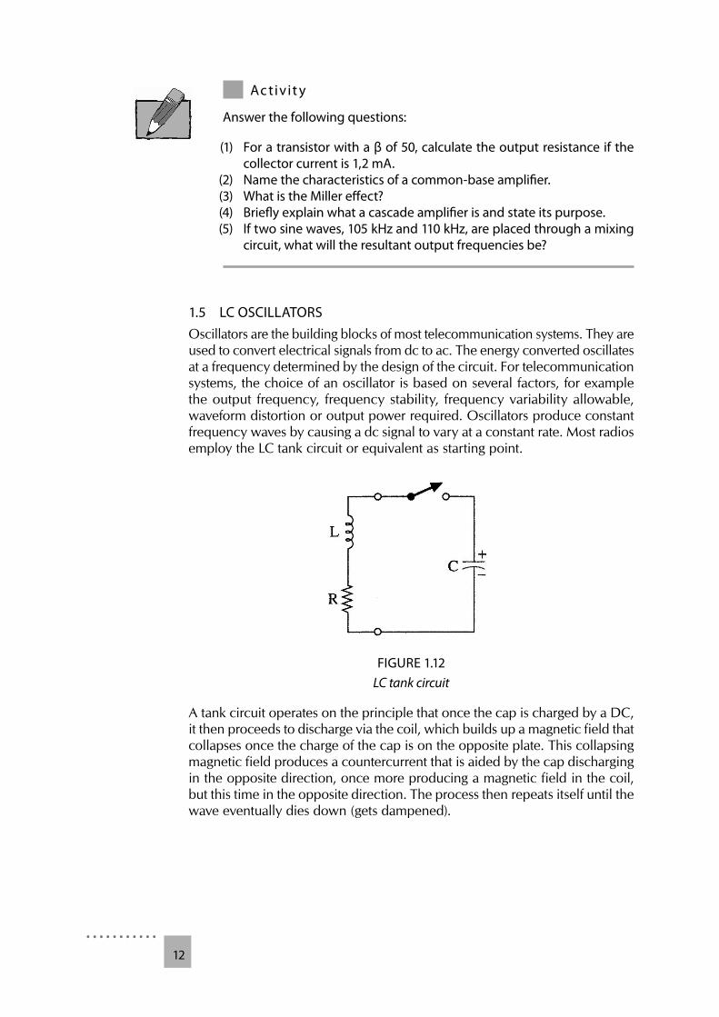
1.5 LC OSCILLATORSOscillators are the building blocks of most telecommunication systems. They are used to convert electrical signals from dc to ac. The energy converted oscillates at a frequency determined by the design of the circuit. For telecommunication systems, the choice of an oscillator is based on several factors, for example the output frequency, frequency stability, frequency variability allowable, waveform distortion or output power required. Oscillators produce constant frequency waves by causing a dc signal to vary at a constant rate. Most radios employ the LC tank circuit or equivalent as starting point.
FIGURE 1.12LC tank circuit
A tank circuit operates on the principle that once the cap is charged by a DC, it then proceeds to discharge via the coil, which builds up a magnetic field that collapses once the charge of the cap is on the opposite plate. This collapsing magnetic field produces a countercurrent that is aided by the cap discharging in the opposite direction, once more producing a magnetic field in the coil, but this time in the opposite direction. The process then repeats itself until the wave eventually dies down (gets dampened).
S T UDY UN I T 1: Intro du c t io n to co mmunic at io n s ys tems
. . . . . . . . . . .R AE 36 01/113
The frequency at which this wave is produced is governed by the formula:
where L is the inductance of the coil in henrys (H) and C is the capacitance of the capacitor in farads (F). The actual values of these coils and capacitors in radios are usually in mH or µH and in µF or pF.
Question:
If a resonant frequency of 604 kHz is required from a simple LC circuit that functions with a 150 µH coil, what size capacitor is required?
Answer:
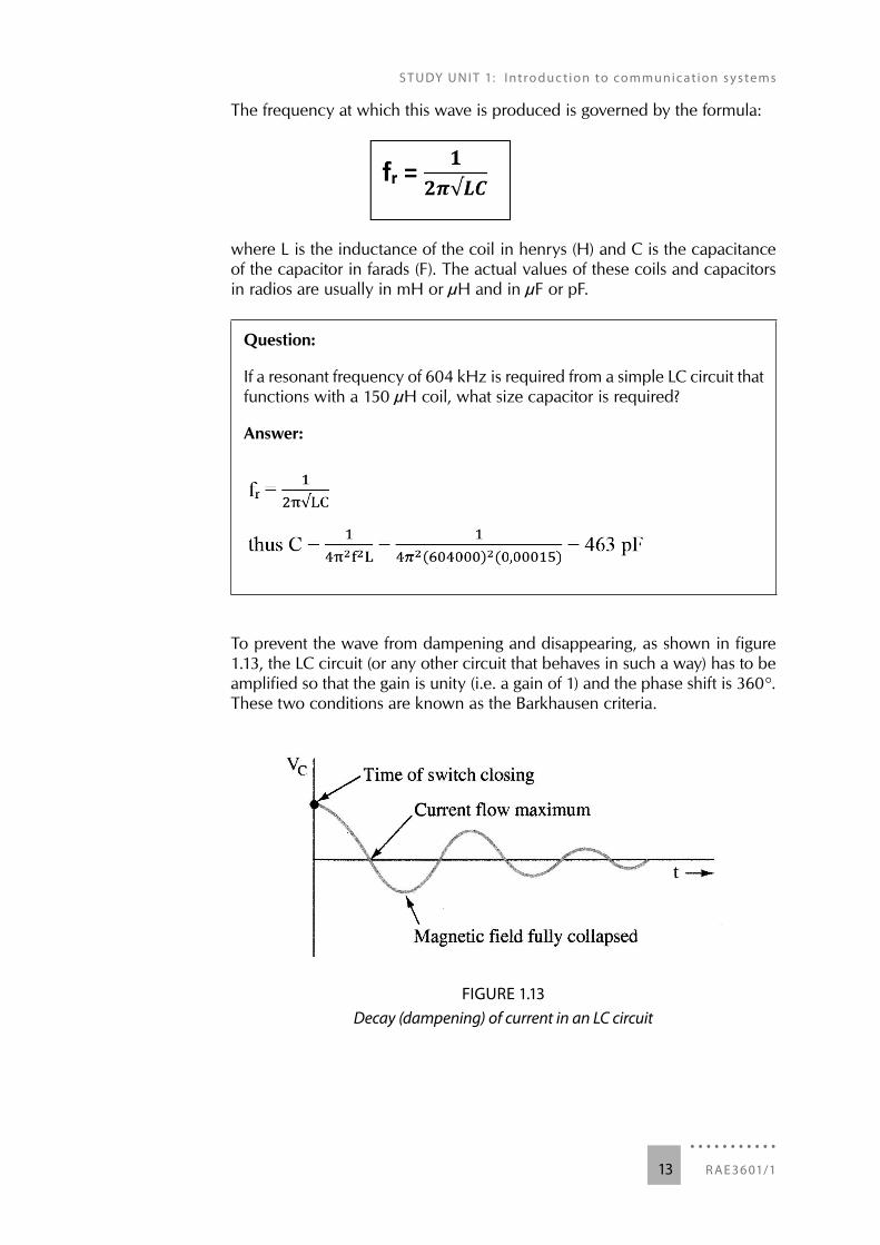
To prevent the wave from dampening and disappearing, as shown in figure 1.13, the LC circuit (or any other circuit that behaves in such a way) has to be amplified so that the gain is unity (i.e. a gain of 1) and the phase shift is 360°. These two conditions are known as the Barkhausen criteria.
FIGURE 1.13Decay (dampening) of current in an LC circuit
. . . . . . . . . . .14
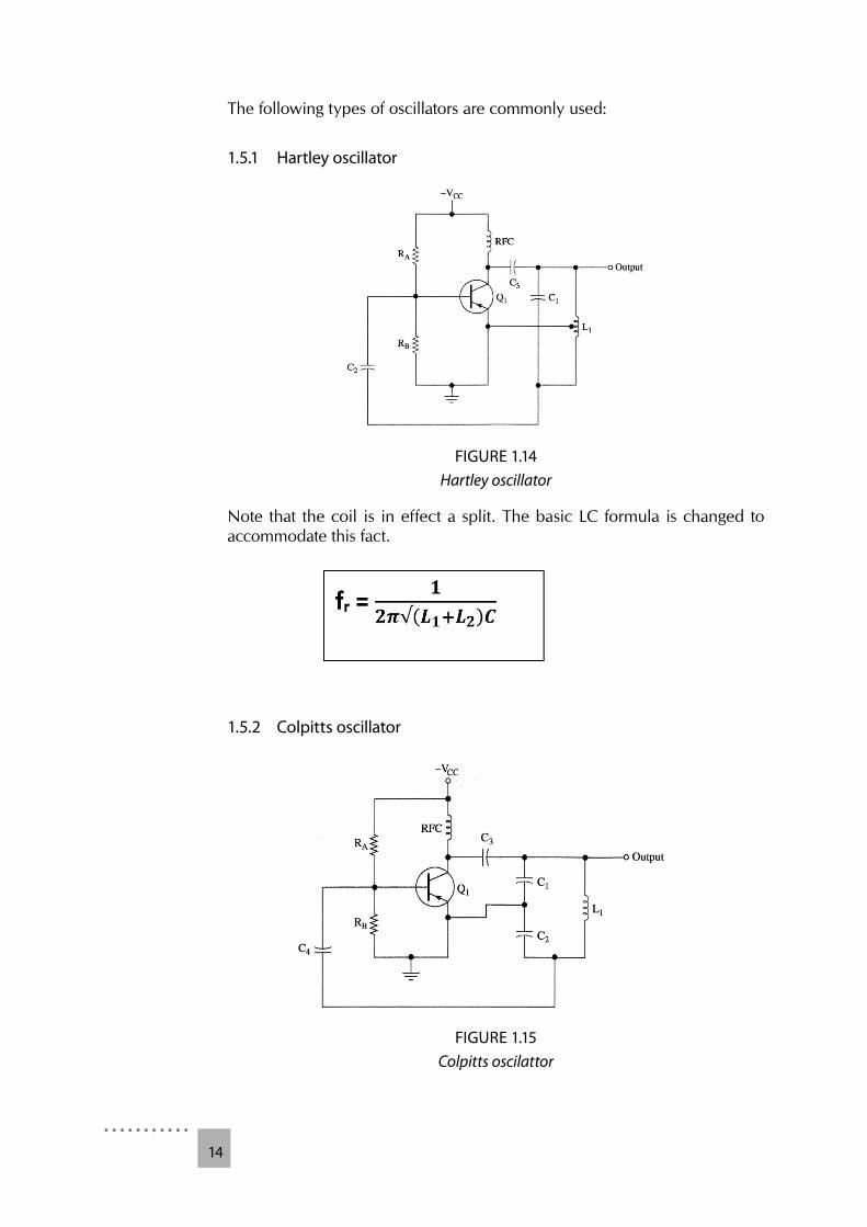
The following types of oscillators are commonly used:
1.5.1 Hartley oscillator
FIGURE 1.14Hartley oscillator
Note that the coil is in effect a split. The basic LC formula is changed to accommodate this fact.
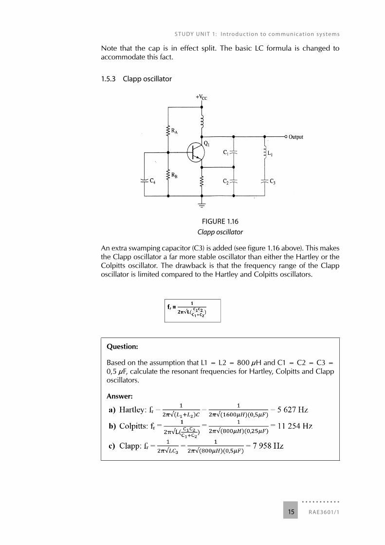
1.5.2 Colpitts oscillator
FIGURE 1.15Colpitts oscilattor
S T UDY UN I T 1: Intro du c t io n to co mmunic at io n s ys tems
. . . . . . . . . . .R AE 36 01/115
Note that the cap is in effect split. The basic LC formula is changed to accommodate this fact.
1.5.3 Clapp oscillator
FIGURE 1.16Clapp oscillator
An extra swamping capacitor (C3) is added (see figure 1.16 above). This makes the Clapp oscillator a far more stable oscillator than either the Hartley or the Colpitts oscillator. The drawback is that the frequency range of the Clapp oscillator is limited compared to the Hartley and Colpitts oscillators.
Question:
Based on the assumption that L1 = L2 = 800 µH and C1 = C2 = C3 = 0,5 µF, calculate the resonant frequencies for Hartley, Colpitts and Clapp oscillators.
Answer:
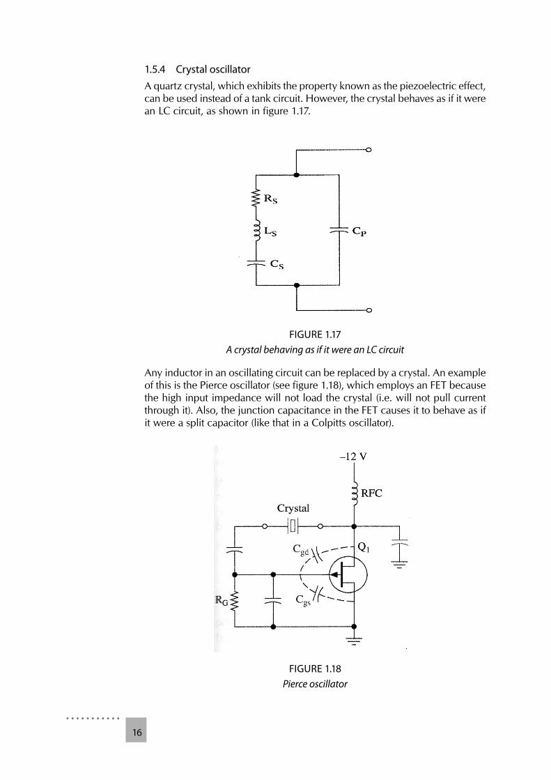
. . . . . . . . . . .16
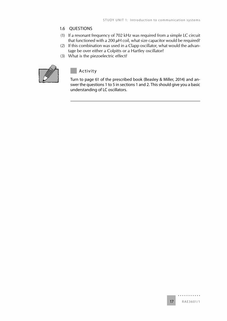
1.5.4 Crystal oscillatorA quartz crystal, which exhibits the property known as the piezoelectric effect, can be used instead of a tank circuit. However, the crystal behaves as if it were an LC circuit, as shown in figure 1.17.
FIGURE 1.17A crystal behaving as if it were an LC circuit
Any inductor in an oscillating circuit can be replaced by a crystal. An example of this is the Pierce oscillator (see figure 1.18), which employs an FET because the high input impedance will not load the crystal (i.e. will not pull current through it). Also, the junction capacitance in the FET causes it to behave as if it were a split capacitor (like that in a Colpitts oscillator).
FIGURE 1.18Pierce oscillator
S T UDY UN I T 1: Intro du c t io n to co mmunic at io n s ys tems
. . . . . . . . . . .R AE 36 01/117
1.6 QUESTIONS(1) If a resonant frequency of 702 kHz was required from a simple LC circuit
that functioned with a 200 µH coil, what size capacitor would be required?(2) If this combination was used in a Clapp oscillator, what would the advan-
tage be over either a Colpitts or a Hartley oscillator?(3) What is the piezoelectric effect?
2Ac tiv it y
Turn to page 61 of the prescribed book (Beasley & Miller, 2014) and an-swer the questions 1 to 5 in sections 1 and 2. This should give you a basic understanding of LC oscillators.
. . . . . . . . . . .18
2S T U D Y U N I T 2
2NOISE
2.1 LEARNING OUTCOMESOnce you have completed this study unit, you should able to do the following:
• Explain noise and perform calculations relating to noise. • Explain different types of noise and give examples of each type. • Explain the effect of noise on communication systems.
2.2 INTRODUCTION TO NOISEElectrical noise is defined as any undesired voltages or currents that may end up in the receiver as unwanted signal. Usually this will cause the desired signal or intelligence to be distorted. The intelligence or desired signal is the signal that is normally needed by the listener. Noise can be classified as external noise or internal noise.
2.2.1 External noiseThere are several types of external noise, including human-made noise and atmospheric noise (noise caused by the atmosphere). Study pages 10 to 13 of the textbook (Beasley & Miller, 2014), where the different types of noise are explained.
2.2.2 Internal noiseInternal noise is introduced by the system into its own circuit. This noise is usually added to the receiver of the system after it has passed through the circuitry of the system. It may occur during the stages of amplification. The types of internal noise are thermal noise and transistor noise. Thermal noise is referred to as Johnson noise or white noise. Please make sure that you understand these terms.
Read page 14 of the textbook (Beasley & Miller, 2014) and pay particular atten-tion to the thermal noise equation shown there. You may expect questions such as the following in the examination:
S T UDY UN I T 2 : N ois e
. . . . . . . . . . .R AE 36 01/119
Example 1: Describe the term noise.
Answer: Electrical noise is any undesired voltages or currents that ultimately end up appearing in the receiver output. A communication receiver is a very sensitive instrument that receives a very small signal; this signal must be greatly amplified before it can possibly drive a speaker.
Example 2: The noise spectral density is given by 4kTR. Determine the bandwidth ∆f of a system in which the noise voltage generated by a 20 kΩ resistor is 20µV rms at room temperature.
Answer: The room temperature is 17 oC, which is equal to 290 K. When we substitute the necessary parameters into the equation, we determine that the bandwidth ∆f = 1.25 MHz.
3Ac tiv it y
Work out example 6 on page 18 and example 7 on page 21 of the text-book (Beasley & Miller, 2014) on your own. Pay particular attention to the formulas for the noise fi gure (NF) and noise ratio (NR). Example 7 shows what happens when noise is amplifi ed through diff erent stages of the telecommunication system.
. . . . . . . . . . .20
3S T U D Y U N I T 3
3AMPLITUDE MODULATION RECEIVERS
3.1 LEARNING OUTCOMESOnce you have completed this study unit, you should be able to do the following:
• Define the sensitivity and selectivity of a radio receiver. • Describe the operation of the diode detector in an AM receiver. • Sketch block diagrams of TRF and superheterodyne receivers. • Calculate image frequencies and explain how they could be suppressed. • Recognise and analyse RF and IF amplifiers. • Explain the need for automatic gain control and describe how it can be
implemented. • Analyse the operation of a complete AM receiver system.
3.2 INTRODUCTIONReceivers are used to convert the modulated signal back to the intelligence signal. The characteristics of a receiver are its sensitivity and selectivity. Sensitivity is defined as the ability of the receiver to make sure that the received signal is driven to an acceptable level. The sensitivity of the receiver is determined by the gain provided by the circuit. Selectivity of the receiver is defined as the ability of the receiver to reject any other frequency and accept only the required frequency.
Read pages 118 to 133 of the textbook (Beasley & Miller, 2014). Pay particular attention to the drawings in the textbook. Attempt to do example 1 (Beasley & Miller, 2014:120).
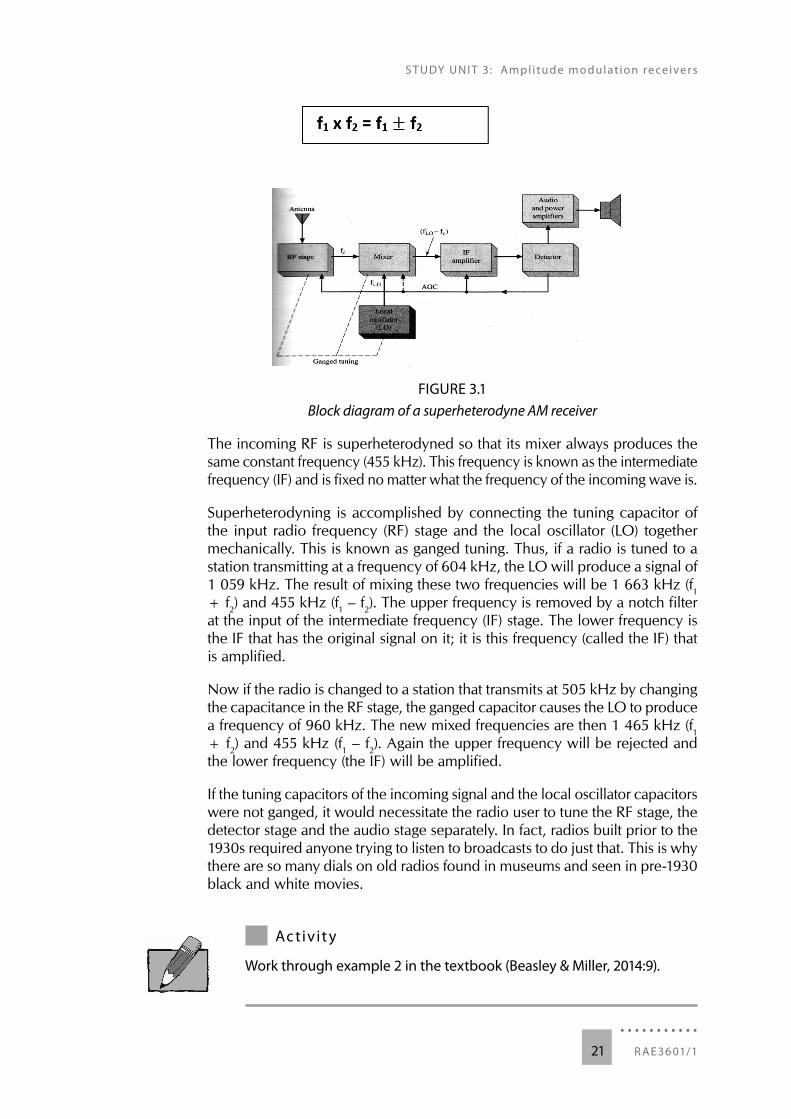
3.3 SUPERHETERODYNE RECEIVERSTurn to page 127 of the textbook and study the information given about superheterodyne receivers (see figure 3.1). Superheterodyne receivers are designed based on variable-selectivity problems in Tuned Radio Frequency (TRF) systems. When two frequencies are combined, they produce the sum and difference of these frequencies.
S T UDY UN I T 3: Amp l i tu de m o dulat io n re ce i ver s
. . . . . . . . . . .R AE 36 01/121
FIGURE 3.1Block diagram of a superheterodyne AM receiver
The incoming RF is superheterodyned so that its mixer always produces the same constant frequency (455 kHz). This frequency is known as the intermediate frequency (IF) and is fixed no matter what the frequency of the incoming wave is.
Superheterodyning is accomplished by connecting the tuning capacitor of the input radio frequency (RF) stage and the local oscillator (LO) together mechanically. This is known as ganged tuning. Thus, if a radio is tuned to a station transmitting at a frequency of 604 kHz, the LO will produce a signal of 1 059 kHz. The result of mixing these two frequencies will be 1 663 kHz (f1 + f2) and 455 kHz (f1 – f2). The upper frequency is removed by a notch filter at the input of the intermediate frequency (IF) stage. The lower frequency is the IF that has the original signal on it; it is this frequency (called the IF) that is amplified.
Now if the radio is changed to a station that transmits at 505 kHz by changing the capacitance in the RF stage, the ganged capacitor causes the LO to produce a frequency of 960 kHz. The new mixed frequencies are then 1 465 kHz (f1 + f2) and 455 kHz (f1 – f2). Again the upper frequency will be rejected and the lower frequency (the IF) will be amplified.
If the tuning capacitors of the incoming signal and the local oscillator capacitors were not ganged, it would necessitate the radio user to tune the RF stage, the detector stage and the audio stage separately. In fact, radios built prior to the 1930s required anyone trying to listen to broadcasts to do just that. This is why there are so many dials on old radios found in museums and seen in pre-1930 black and white movies.
4Ac tiv it y
Work through example 2 in the textbook (Beasley & Miller, 2014:9).
. . . . . . . . . . .22
3.4 TUNING RANGEThe tuning range is the range of frequencies that a radio receiver can be tuned into. Commercial radio stations range from about 500 kHz to just over 1 600 kHz, while emergency services, police and air traffic control are transmitted at slightly higher frequencies.
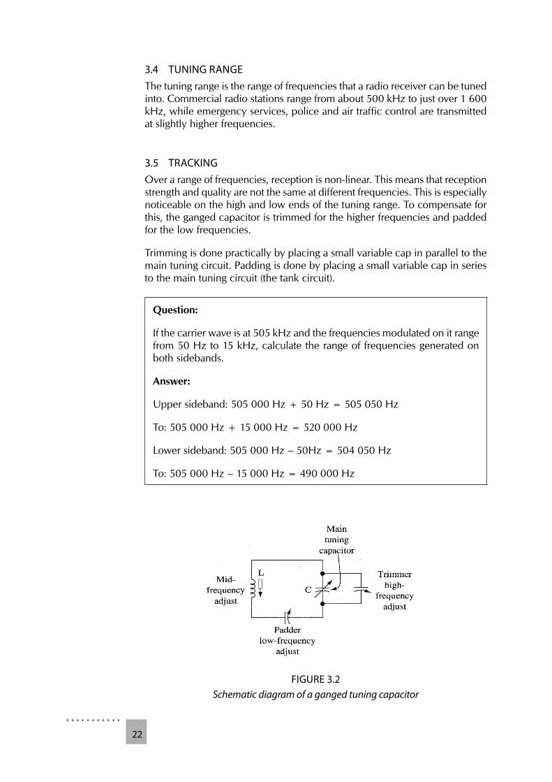
3.5 TRACKINGOver a range of frequencies, reception is non-linear. This means that reception strength and quality are not the same at different frequencies. This is especially noticeable on the high and low ends of the tuning range. To compensate for this, the ganged capacitor is trimmed for the higher frequencies and padded for the low frequencies.
Trimming is done practically by placing a small variable cap in parallel to the main tuning circuit. Padding is done by placing a small variable cap in series to the main tuning circuit (the tank circuit).
Question:
If the carrier wave is at 505 kHz and the frequencies modulated on it range from 50 Hz to 15 kHz, calculate the range of frequencies generated on both sidebands.
Answer:
Upper sideband: 505 000 Hz + 50 Hz = 505 050 Hz
To: 505 000 Hz + 15 000 Hz = 520 000 Hz
Lower sideband: 505 000 Hz – 50Hz = 504 050 Hz
To: 505 000 Hz – 15 000 Hz = 490 000 Hz
FIGURE 3.2Schematic diagram of a ganged tuning capacitor
S T UDY UN I T 3: Amp l i tu de m o dulat io n re ce i ver s
. . . . . . . . . . .R AE 36 01/123
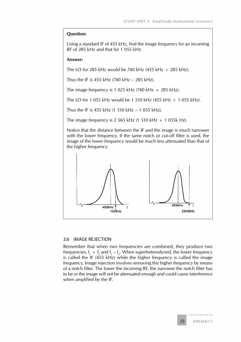
Question:
Using a standard IF of 455 kHz, find the image frequency for an incoming RF of 285 kHz and that for 1 055 kHz.
Answer:
The LO for 285 kHz would be 740 kHz (455 kHz + 285 kHz).
Thus the IF is 455 kHz (740 kHz – 285 kHz).
The image frequency is 1 025 kHz (740 kHz + 285 kHz).
The LO for 1 055 kHz would be 1 510 kHz (455 kHz + 1 055 kHz).
Thus the IF is 455 kHz (1 510 kHz – 1 055 kHz).
The image frequency is 2 565 kHz (1 510 kHz + 1 055k Hz).
Notice that the distance between the IF and the image is much narrower with the lower frequency. If the same notch or cut-off filter is used, the image of the lower frequency would be much less attenuated than that of the higher frequency.
3.6 IMAGE REJECTIONRemember that when two frequencies are combined, they produce two frequencies, f1 + f2 and f1 – f2. When superheterodyned, the lower frequency is called the IF (455 kHz) while the higher frequency is called the image frequency. Image rejection involves removing this higher frequency by means of a notch filter. The lower the incoming RF, the narrower the notch filter has to be or the image will not be attenuated enough and could cause interference when amplified by the IF.
. . . . . . . . . . .24
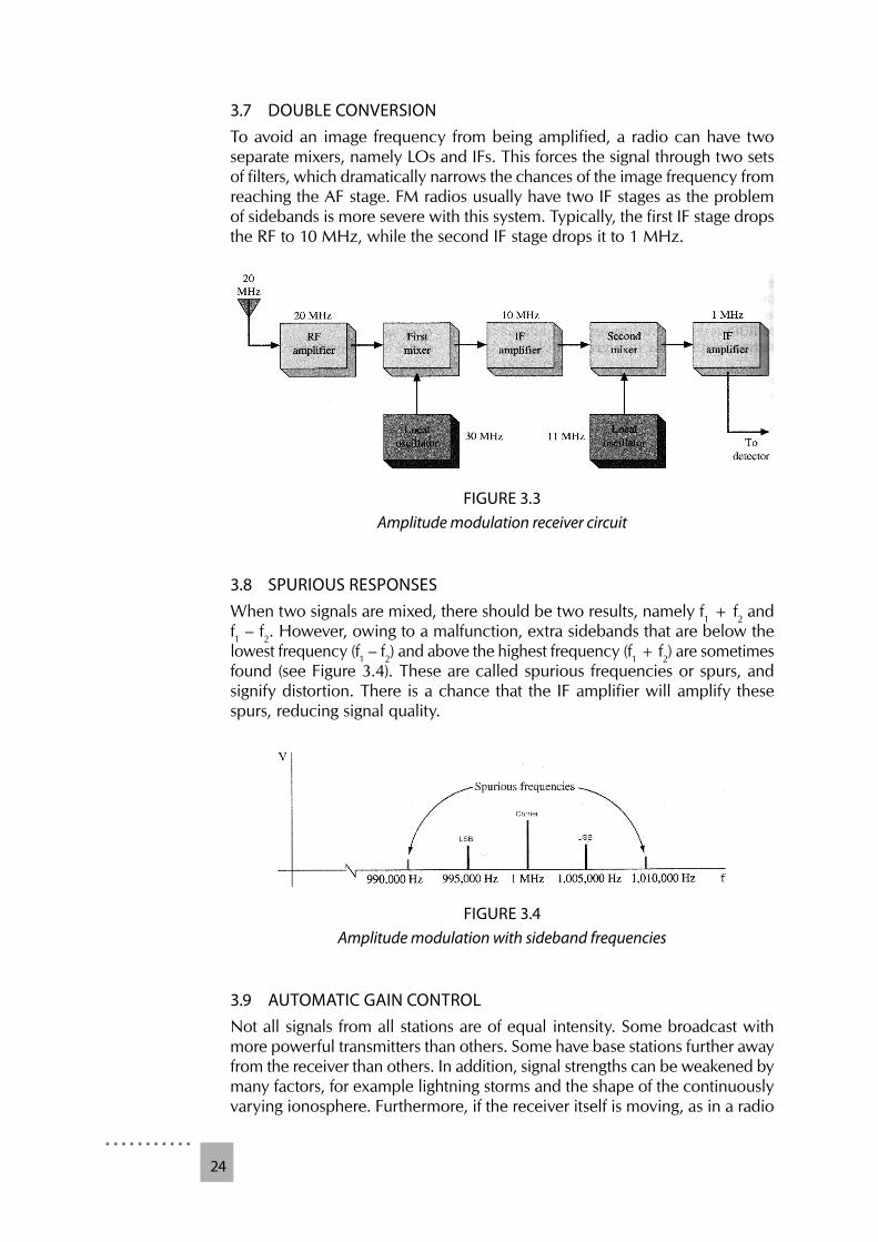
3.7 DOUBLE CONVERSIONTo avoid an image frequency from being amplified, a radio can have two separate mixers, namely LOs and IFs. This forces the signal through two sets of filters, which dramatically narrows the chances of the image frequency from reaching the AF stage. FM radios usually have two IF stages as the problem of sidebands is more severe with this system. Typically, the first IF stage drops the RF to 10 MHz, while the second IF stage drops it to 1 MHz.
FIGURE 3.3Amplitude modulation receiver circuit
3.8 SPURIOUS RESPONSESWhen two signals are mixed, there should be two results, namely f1 + f2 and f1 – f2. However, owing to a malfunction, extra sidebands that are below the lowest frequency (f1 – f2) and above the highest frequency (f1 + f2) are sometimes found (see Figure 3.4). These are called spurious frequencies or spurs, and signify distortion. There is a chance that the IF amplifier will amplify these spurs, reducing signal quality.
FIGURE 3.4Amplitude modulation with sideband frequencies
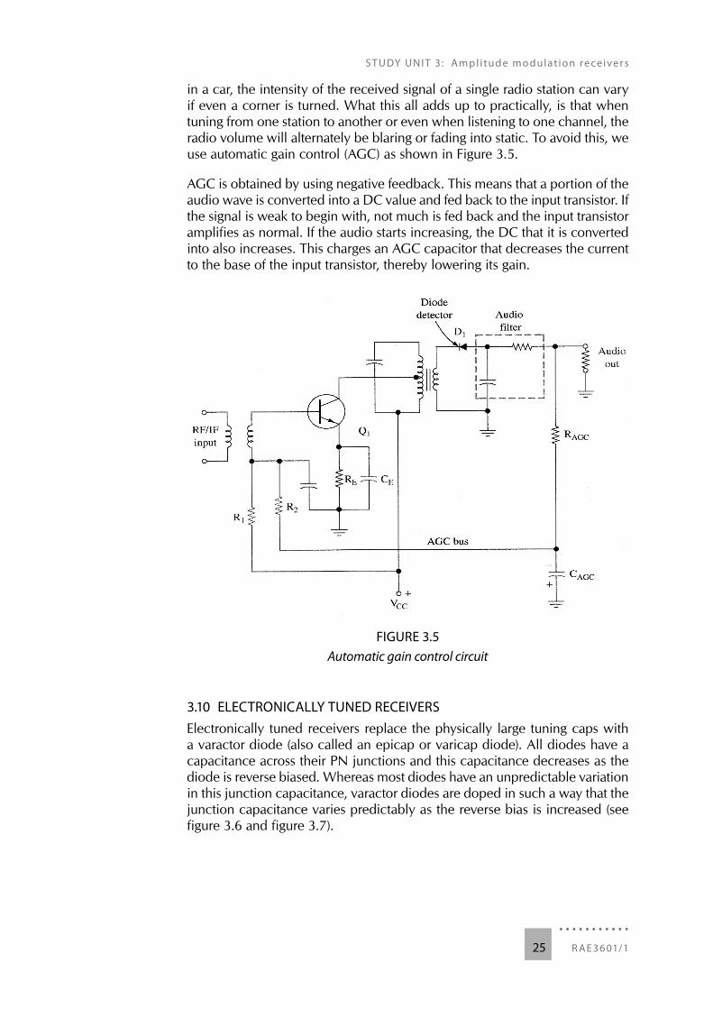
3.9 AUTOMATIC GAIN CONTROLNot all signals from all stations are of equal intensity. Some broadcast with more powerful transmitters than others. Some have base stations further away from the receiver than others. In addition, signal strengths can be weakened by many factors, for example lightning storms and the shape of the continuously varying ionosphere. Furthermore, if the receiver itself is moving, as in a radio
S T UDY UN I T 3: Amp l i tu de m o dulat io n re ce i ver s
. . . . . . . . . . .R AE 36 01/125
in a car, the intensity of the received signal of a single radio station can vary if even a corner is turned. What this all adds up to practically, is that when tuning from one station to another or even when listening to one channel, the radio volume will alternately be blaring or fading into static. To avoid this, we use automatic gain control (AGC) as shown in Figure 3.5.
AGC is obtained by using negative feedback. This means that a portion of the audio wave is converted into a DC value and fed back to the input transistor. If the signal is weak to begin with, not much is fed back and the input transistor amplifies as normal. If the audio starts increasing, the DC that it is converted into also increases. This charges an AGC capacitor that decreases the current to the base of the input transistor, thereby lowering its gain.
FIGURE 3.5Automatic gain control circuit
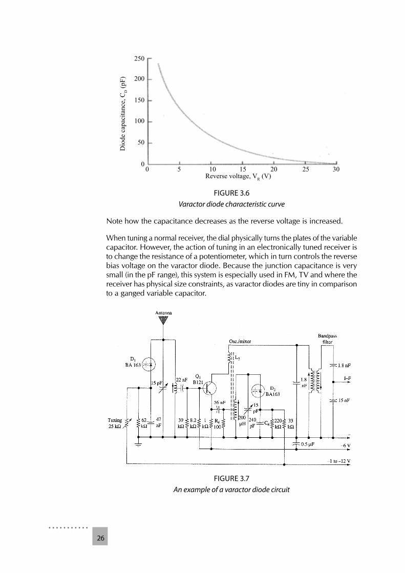
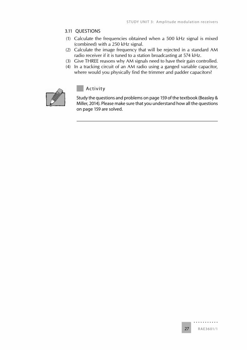
3.10 ELECTRONICALLY TUNED RECEIVERSElectronically tuned receivers replace the physically large tuning caps with a varactor diode (also called an epicap or varicap diode). All diodes have a capacitance across their PN junctions and this capacitance decreases as the diode is reverse biased. Whereas most diodes have an unpredictable variation in this junction capacitance, varactor diodes are doped in such a way that the junction capacitance varies predictably as the reverse bias is increased (see figure 3.6 and figure 3.7).
. . . . . . . . . . .26
Reverse voltage, VR (V)
Dio
de c
apac
itanc
e, C
D (p
F)
250
200
150
100
50
00 5 10 15 20 25 30
FIGURE 3.6Varactor diode characteristic curve
Note how the capacitance decreases as the reverse voltage is increased.
When tuning a normal receiver, the dial physically turns the plates of the variable capacitor. However, the action of tuning in an electronically tuned receiver is to change the resistance of a potentiometer, which in turn controls the reverse bias voltage on the varactor diode. Because the junction capacitance is very small (in the pF range), this system is especially used in FM, TV and where the receiver has physical size constraints, as varactor diodes are tiny in comparison to a ganged variable capacitor.
FIGURE 3.7An example of a varactor diode circuit
S T UDY UN I T 3: Amp l i tu de m o dulat io n re ce i ver s
. . . . . . . . . . .R AE 36 01/127
3.11 QUESTIONS(1) Calculate the frequencies obtained when a 500 kHz signal is mixed
(combined) with a 250 kHz signal.(2) Calculate the image frequency that will be rejected in a standard AM
radio receiver if it is tuned to a station broadcasting at 574 kHz.(3) Give THREE reasons why AM signals need to have their gain controlled.(4) In a tracking circuit of an AM radio using a ganged variable capacitor,
where would you physically find the trimmer and padder capacitors?
5Ac tiv it y
Study the questions and problems on page 159 of the textbook (Beasley & Miller, 2014). Please make sure that you understand how all the questions on page 159 are solved.
. . . . . . . . . . .28
4S T U D Y U N I T 4
4AMPLITUDE MODULATION TRANSMITTERS
4.1 LEARNING OUTCOMESOnce you have completed this study unit, you should be able to do the following:
• Describe the process of amplitude modulation. • Sketch AM waveforms with various modulation indexes. • Explain the difference between a sideband and side frequency. • Analyse and perform various power, voltage and current calculations in
AM systems. • Explain the circuits used to generate AM. • Determine and analyse the high-level and low-level modulation and systems
from schematics and block diagrams.
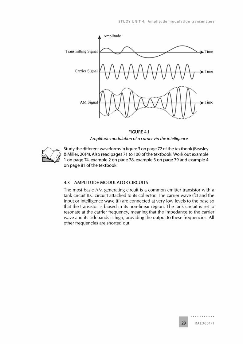
4.2 INTRODUCTIONAmplitude modulation is the process of combining a low-frequency signal called the intelligence and a high-frequency signal called the carrier. This process is called modulation. Modulation of the carrier signal by the intelligence allows the intelligence to be transported across the medium without any interference. The intelligence will modulate the carrier into three different characteristics. The carrier can be modulated by varying either the amplitude, the frequency or its phase. Amplitude modulation involves the variation of a carrier’s amplitude by the intelligence to result in what is known as amplitude modulation. The modulation of the carrier by the intelligence is usually done through a non-linear device to form the following:
• a dc level • components of each of the two frequencies • components of the sum and differences of the two original frequencies • harmonics of the two original frequencies
S T UDY UN I T 4 : Amp l i tu de m o dulat io n t r ansmit ter s
. . . . . . . . . . .R AE 36 01/129
Amplitude
Transmitting Signal
Carrier Signal
AM Signal
Time
Time
Time
FIGURE 4.1Amplitude modulation of a carrier via the intelligence
Study the different waveforms in figure 3 on page 72 of the textbook (Beasley & Miller, 2014). Also read pages 71 to 100 of the textbook. Work out example 1 on page 74, example 2 on page 78, example 3 on page 79 and example 4 on page 81 of the textbook.
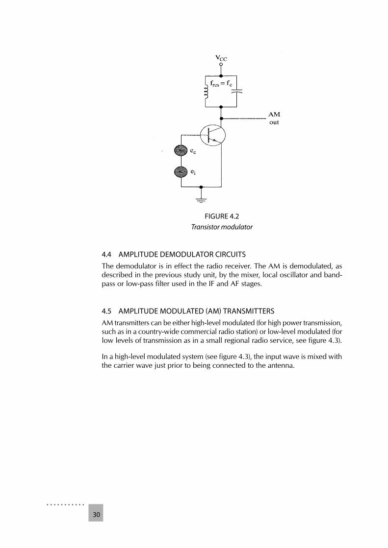
4.3 AMPLITUDE MODULATOR CIRCUITSThe most basic AM generating circuit is a common emitter transistor with a tank circuit (LC circuit) attached to its collector. The carrier wave (fc) and the input or intelligence wave (fi) are connected at very low levels to the base so that the transistor is biased in its non-linear region. The tank circuit is set to resonate at the carrier frequency, meaning that the impedance to the carrier wave and its sidebands is high, providing the output to these frequencies. All other frequencies are shorted out.
. . . . . . . . . . .30
FIGURE 4.2Transistor modulator
4.4 AMPLITUDE DEMODULATOR CIRCUITSThe demodulator is in effect the radio receiver. The AM is demodulated, as described in the previous study unit, by the mixer, local oscillator and band-pass or low-pass filter used in the IF and AF stages.
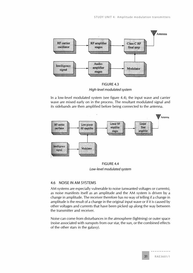
4.5 AMPLITUDE MODULATED (AM) TRANSMITTERSAM transmitters can be either high-level modulated (for high power transmission, such as in a country-wide commercial radio station) or low-level modulated (for low levels of transmission as in a small regional radio service, see figure 4.3).
In a high-level modulated system (see figure 4.3), the input wave is mixed with the carrier wave just prior to being connected to the antenna.
S T UDY UN I T 4 : Amp l i tu de m o dulat io n t r ansmit ter s
. . . . . . . . . . .R AE 36 01/131
FIGURE 4.3High-level modulated system
In a low-level modulated system (see figure 4.4), the input wave and carrier wave are mixed early on in the process. The resultant modulated signal and its sidebands are then amplified before being connected to the antenna.
FIGURE 4.4Low-level modulated system
4.6 NOISE IN AM SYSTEMSAM systems are especially vulnerable to noise (unwanted voltages or currents), as noise manifests itself as an amplitude and the AM system is driven by a change in amplitude. The receiver therefore has no way of telling if a change in amplitude is the result of a change in the original input wave or if it is caused by other voltages and currents that have been picked up along the way between the transmitter and receiver.
Noise can come from disturbances in the atmosphere (lightning) or outer space (noise associated with sunspots from our star, the sun, or the combined effects of the other stars in the galaxy).
. . . . . . . . . . .32
Noise can also be generated by machines such as lawn mowers, starter motors and even fluorescent lights. Temperature variations in the receiver itself are a further source of noise.
4.7 QUESTIONS(1) What is the difference between a high-level modulated system and a
low-level modulated system? Name an application of each type.(2) List the main sources of noise in an AM system.(3) The following audio signal and its carrier waveform are given:
Aa (t) = 3 + 1,5 sin (2π × 1500 × t)Ac (t) = 6,0 sin (2π× 50, 000 × t)
3.1 Plot both these waveforms in a single plot.3.2 Construct an AM modulated wave.3.3 Determine the modulation factor and percentage modulation.3.4 What are the frequencies of the audio signal and the carrier?
. . . . . . . . . . .R AE 36 01/133
5S T U D Y U N I T 5
5THE SINGLE SIDEBAND (SSB)
5.1 LEARNING OUTCOMESOnce you have completed this study unit, you should be able to do the following:
• Interpret and describe how the AM generator could be modified to provide an SSB.
• Explain the different SSB types and compare their advantages to the advantages of AM.
• Explain the difference between a sideband and side frequency. • Describe and explain the circuits that are used for an SSB. • Describe the different methods that are used to demodulate SSBs. • Draw and analyse phase shift methods in SSBs.
5.2 SINGLE-SIDEBAND PRINCIPLESSingle-sideband (SSB) modulation means that only one of the sidebands in an AM modulated signal is transmitted, such as when using a walkie-talkie system. Instead of transmitting the entire signal (carrier and both sidebands), the carrier and one of the sidebands are removed.
This means the quality of the received signal is very poor if you try to transmit music like this, but sending intelligible voice signals is nonetheless possible. SSB modulation allows a far lower power consumption during transmission. As a result, the equipment required to transmit needs a far smaller power supply and a massive weight reduction is achieved – both factors that are essential for a mobile communication system.
Another advantage of only sending one sideband is that there is no chance of the other sideband interfering with it should the two go out of phase owing to a phase changing reflection.
Not all SSB systems completely eliminate the carrier wave; some only suppress it to a limited degree. This helps with sound quality and gives the receiver automatic gain control. In such cases, the suppressed carrier wave is referred to as the pilot wave.
Since one of the sidebands are removed, the space in the spectrum that would have been taken up by it can be utilised for a different transmission.
. . . . . . . . . . .34
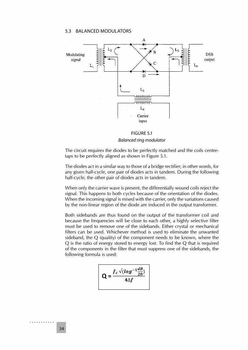
5.3 BALANCED MODULATORS
FIGURE 5.1Balanced ring modulator
The circuit requires the diodes to be perfectly matched and the coils centre-taps to be perfectly aligned as shown in Figure 5.1.
The diodes act in a similar way to those of a bridge rectifier; in other words, for any given half-cycle, one pair of diodes acts in tandem. During the following half-cycle, the other pair of diodes acts in tandem.
When only the carrier wave is present, the differentially wound coils reject the signal. This happens to both cycles because of the orientation of the diodes. When the incoming signal is mixed with the carrier, only the variations caused by the non-linear region of the diode are induced in the output transformer.
Both sidebands are thus found on the output of the transformer coil and because the frequencies will be close to each other, a highly selective filter must be used to remove one of the sidebands. Either crystal or mechanical filters can be used. Whichever method is used to eliminate the unwanted sideband, the Q (quality) of the component needs to be known, where the Q is the ratio of energy stored to energy lost. To find the Q that is required of the components in the filter that must suppress one of the sidebands, the following formula is used:
S T UDY UN I T 5: T h e s ingl e s ideb an d (ssb)
. . . . . . . . . . .R AE 36 01/135
Where:
fc = carrier frequency
∆f = the separation between the sidebands
dB = the amount of suppression that is required
Question:
The unwanted sideband of an SSB radio must be suppressed by 100 dB in relation to the used sideband. If the carrier has a frequency of 95 kHz and the separation between the sidebands is 400 Hz, calculate the Q (quality) of the filter needed.
Answer:
Study pages 166 to 169 of the textbook (Beasley & Miller, 2014). Pay particular attention to power distribution in sideband transmission, types of sideband transmission and the advantages of sideband transmission. Also look at the circuits that are used to generate single-sideband transmission.
Study pages 182 to 193 of the textbook (Beasley & Miller, 2014). Pay particular attention to SSB receivers and transmitters.
Complete example 2 on page 178 and example 4 on page 187 of the textbook (Beasley & Miller, 2014).
5.4 QUESTIONS(1) List the advantages of transmitting in SSB mode.(2) Why can the sound quality be improved by adding a pilot wave?(3) Describe how a balanced ring modulator combines the frequencies while
suppressing the carrier wave.(4) The unwanted sideband of an SSB radio must be suppressed by 800 dB
in relation to the used sideband. If the carrier has a frequency of 950 kHz and the separation between the sidebands is 400 Hz, calculate the Q (quality) of the fi lter needed.
. . . . . . . . . . .36
6S T U D Y U N I T 6
6FREQUENCY MODULATION TRANSMITTERS AND RECEIVERS
6.1 LEARNING OUTCOMESOnce you have completed this study unit, you should be able to do the following:
• Define and describe two categories of angle modulation. • Analyse FM signals with reference to modulation indices, sidebands and
power, and perform calculations relating to FM signals. • Describe the noise suppression capabilities of FM and explain how they
relate to the capture effect and pre-emphasis. • Describe and illustrate the various schemes and circuits used to generate FM. • Explain how a PLL can be used to generate FM. • Explain the multiplexing technique that is used to add stereo to standard
FM broadcast systems. • Describe the operation of an FM receiving system and explain how it differs
from an AM receiving system. • Draw a slope detector schematic and explain how it can provide the required
response to the modulating signal amplitude and frequency. • Describe the operation of the PLL and explain how it can be utilised as an
FM discriminator. • Describe a complete stereo broadcast band receiver and explain how it
works. • Draw a complete FM receiver schematic and explain how it works.
Aside from mixing frequencies so that the amplitude of the carrier is changed in proportion to that of the modulating wave, the phase and the frequency of the carrier wave can be changed as well. Phase modulation (PM) or frequency modulation (FM) is collectively known as angle modulation. Read pages 206 to 253 of the textbook (Beasley & Miller, 2014)
6.2 FREQUENCY MODULATIONFM transports the voice signal (intelligence signal) by changing the frequency (as opposed to the amplitude) of a carrier wave. This variation about the central carrier frequency is known as the frequency deviation (δ). The higher the amplitude of the voice signal, the more the frequency deviates. The higher
S T UDY UN I T 6 : Fre qu enc y m o dulat io n t r ansmit ter s an d re ce i ver s
. . . . . . . . . . .R AE 36 01/137
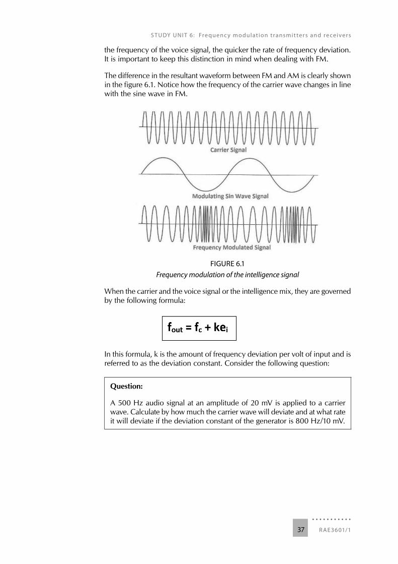
the frequency of the voice signal, the quicker the rate of frequency deviation. It is important to keep this distinction in mind when dealing with FM.
The difference in the resultant waveform between FM and AM is clearly shown in the figure 6.1. Notice how the frequency of the carrier wave changes in line with the sine wave in FM.
FIGURE 6.1Frequency modulation of the intelligence signal
When the carrier and the voice signal or the intelligence mix, they are governed by the following formula:
In this formula, k is the amount of frequency deviation per volt of input and is referred to as the deviation constant. Consider the following question:
Question:
A 500 Hz audio signal at an amplitude of 20 mV is applied to a carrier wave. Calculate by how much the carrier wave will deviate and at what rate it will deviate if the deviation constant of the generator is 800 Hz/10 mV.
. . . . . . . . . . .38
Answer:
First the amount of deviation around the central carrier must be calculated. Remember that the deviation will occur on both sides of the carrier wave.
This means that the carrier will increase by 1,6 kHz above its value and decrease by 1,6 kHz below its value.
The rate at which it will do this will be the same as the frequency of the modulating wave, namely 500 Hz.
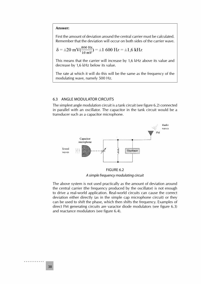
6.3 ANGLE MODULATOR CIRCUITSThe simplest angle modulation circuit is a tank circuit (see figure 6.2) connected in parallel with an oscillator. The capacitor in the tank circuit would be a transducer such as a capacitor microphone.
FIGURE 6.2A simple frequency modulating circuit
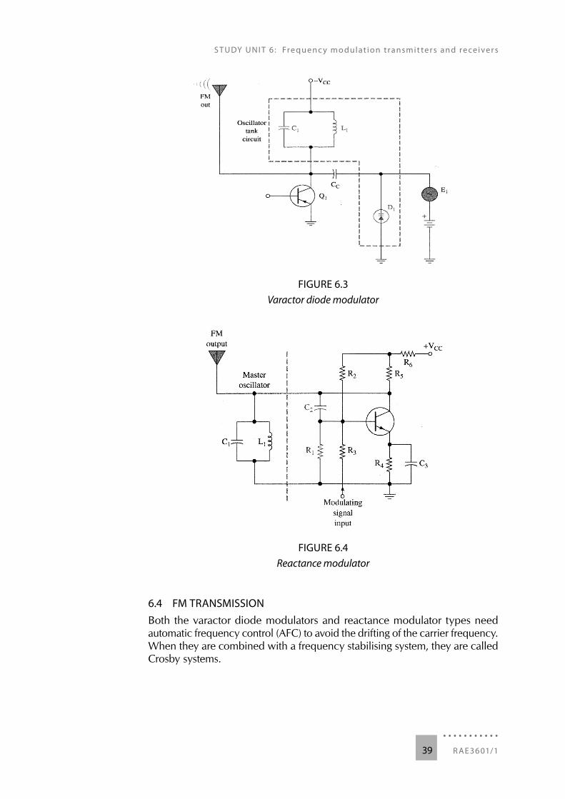
The above system is not used practically as the amount of deviation around the central carrier (the frequency produced by the oscillator) is not enough to drive a real-world application. Real-world circuits can cause the correct deviation either directly (as in the simple cap microphone circuit) or they can be used to shift the phase, which then shifts the frequency. Examples of direct FM generating circuits are varactor diode modulators (see figure 6.3) and reactance modulators (see figure 6.4).
S T UDY UN I T 6 : Fre qu enc y m o dulat io n t r ansmit ter s an d re ce i ver s
. . . . . . . . . . .R AE 36 01/139
FIGURE 6.3Varactor diode modulator
FIGURE 6.4Reactance modulator
6.4 FM TRANSMISSIONBoth the varactor diode modulators and reactance modulator types need automatic frequency control (AFC) to avoid the drifting of the carrier frequency. When they are combined with a frequency stabilising system, they are called Crosby systems.
. . . . . . . . . . .40
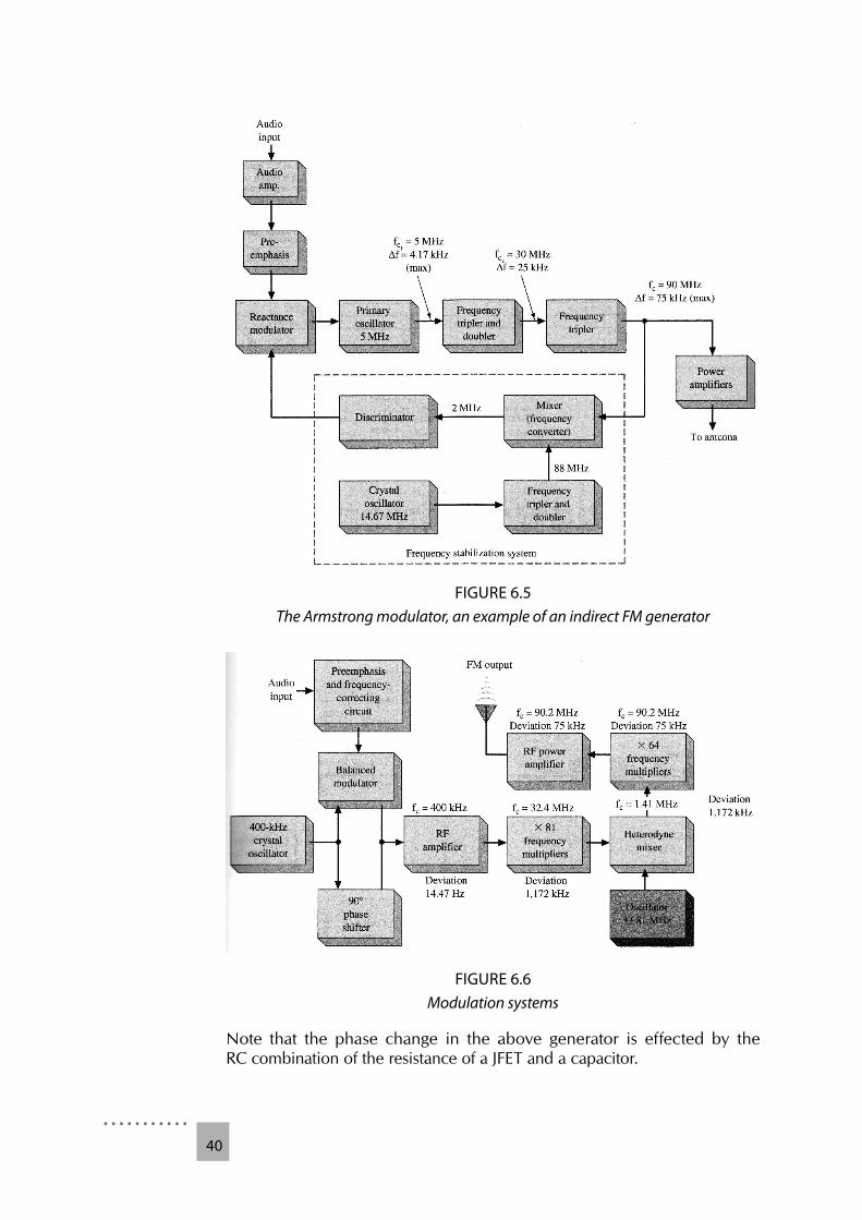
FIGURE 6.5The Armstrong modulator, an example of an indirect FM generator
FIGURE 6.6Modulation systems
Note that the phase change in the above generator is effected by the RC combination of the resistance of a JFET and a capacitor.
S T UDY UN I T 6 : Fre qu enc y m o dulat io n t r ansmit ter s an d re ce i ver s
. . . . . . . . . . .R AE 36 01/141
Turn to page 209 of the textbook (Beasley & Miller, 2014) and do example 1. Then do example 2 on page 210; examples 3 and 4 on page 214; example 5 on page 215; and example 6 on page 218.
Answer the questions in sections 1, 2 and 3 on page 253 of the textbook (Beasley & Miller, 2014).
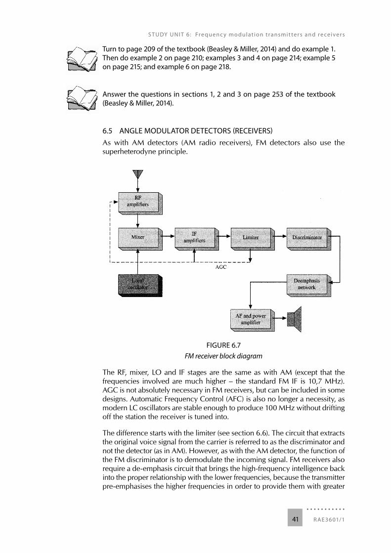
6.5 ANGLE MODULATOR DETECTORS (RECEIVERS)As with AM detectors (AM radio receivers), FM detectors also use the superheterodyne principle.
FIGURE 6.7FM receiver block diagram
The RF, mixer, LO and IF stages are the same as with AM (except that the frequencies involved are much higher – the standard FM IF is 10,7 MHz). AGC is not absolutely necessary in FM receivers, but can be included in some designs. Automatic Frequency Control (AFC) is also no longer a necessity, as modern LC oscillators are stable enough to produce 100 MHz without drifting off the station the receiver is tuned into.
The difference starts with the limiter (see section 6.6). The circuit that extracts the original voice signal from the carrier is referred to as the discriminator and not the detector (as in AM). However, as with the AM detector, the function of the FM discriminator is to demodulate the incoming signal. FM receivers also require a de-emphasis circuit that brings the high-frequency intelligence back into the proper relationship with the lower frequencies, because the transmitter pre-emphasises the higher frequencies in order to provide them with greater
. . . . . . . . . . .42
noise immunity. Once the original voice signal has been reproduced, the FM receiver works in the same way as an AM receiver.
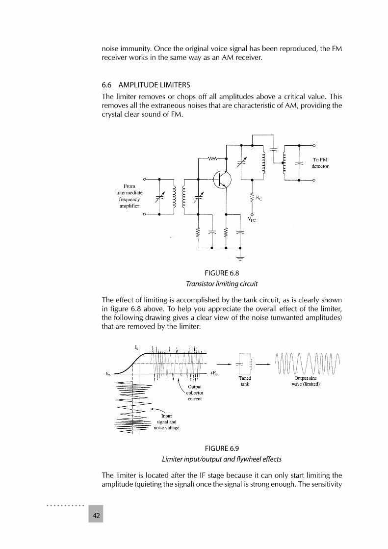
6.6 AMPLITUDE LIMITERSThe limiter removes or chops off all amplitudes above a critical value. This removes all the extraneous noises that are characteristic of AM, providing the crystal clear sound of FM.
FIGURE 6.8Transistor limiting circuit
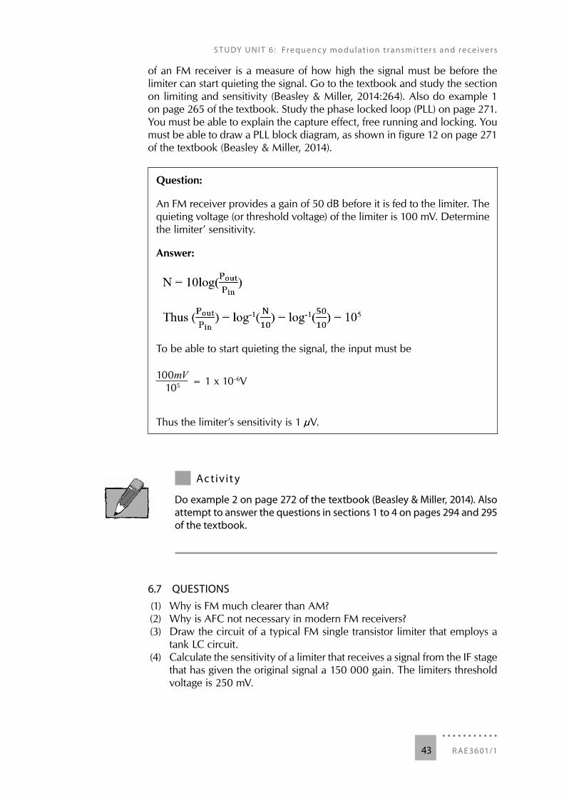
The effect of limiting is accomplished by the tank circuit, as is clearly shown in figure 6.8 above. To help you appreciate the overall effect of the limiter, the following drawing gives a clear view of the noise (unwanted amplitudes) that are removed by the limiter:
FIGURE 6.9Limiter input/output and flywheel effects
The limiter is located after the IF stage because it can only start limiting the amplitude (quieting the signal) once the signal is strong enough. The sensitivity
S T UDY UN I T 6 : Fre qu enc y m o dulat io n t r ansmit ter s an d re ce i ver s
. . . . . . . . . . .R AE 36 01/143
of an FM receiver is a measure of how high the signal must be before the limiter can start quieting the signal. Go to the textbook and study the section on limiting and sensitivity (Beasley & Miller, 2014:264). Also do example 1 on page 265 of the textbook. Study the phase locked loop (PLL) on page 271. You must be able to explain the capture effect, free running and locking. You must be able to draw a PLL block diagram, as shown in figure 12 on page 271 of the textbook (Beasley & Miller, 2014).
Question:
An FM receiver provides a gain of 50 dB before it is fed to the limiter. The quieting voltage (or threshold voltage) of the limiter is 100 mV. Determine the limiter’ sensitivity.
Answer:
To be able to start quieting the signal, the input must be
100mV 105
= 1 x 10 -6V
Thus the limiter’s sensitivity is 1 µV.
6Ac tiv it y
Do example 2 on page 272 of the textbook (Beasley & Miller, 2014). Also attempt to answer the questions in sections 1 to 4 on pages 294 and 295 of the textbook.
6.7 QUESTIONS(1) Why is FM much clearer than AM?(2) Why is AFC not necessary in modern FM receivers?(3) Draw the circuit of a typical FM single transistor limiter that employs a
tank LC circuit.(4) Calculate the sensitivity of a limiter that receives a signal from the IF stage
that has given the original signal a 150 000 gain. The limiters threshold voltage is 250 mV.
. . . . . . . . . . .44
7S T U D Y U N I T 7
7INTRODUCTION TO DIGITAL COMMUNICATION
7.1 LEARNING OUTCOMESOnce you have competed this study unit, you should be able to do the following:
• Describe the quantisation process in a PCM system. • Calculate the Nyquist sampling frequency and explain the techniques
involved. • Describe and explain quantisation levels, aliasing, quantisation errors and
quantisation noise. • Explain pulse amplitude modulation (PAM), flat-top sampling and natural
sampling.
7.2 DIGITAL COMMUNICATIONSDigital communication requires that intelligence should first be converted from an analogue signal to a digital signal before it is broadcast. At the receiver, the intelligence is then converted back into an analogue signal. The great advantage of this is that most of the noise associated with transmitted signals can be eliminated.
Using a digital communications system, the digitised signal is usually processed by encoding it in a certain format before transmission, and then decoding it at the receiver.
Terminology
Before we discuss digital transmission systems, please make sure that you fully understand the following technical terms:
Bit
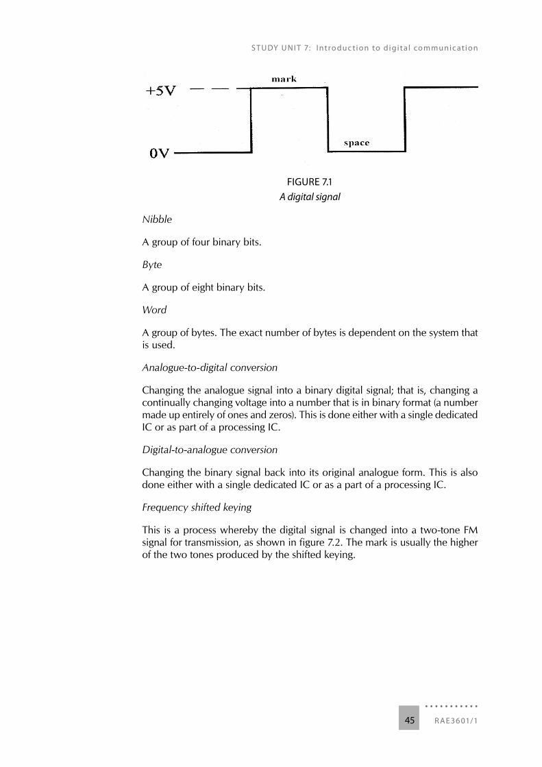
A single piece of information. It can either be a ‘1’ (a set voltage, usually +5 V) or a ‘0’ (0 V or earth). The ‘1’ is often referred to as a mark, whereas the ‘0’ is often referred to as a space (see figure 7.1).
S T UDY UN I T 7: Intro du c t io n to digi t a l co mmunic at io n
. . . . . . . . . . .R AE 36 01/145
FIGURE 7.1A digital signal
Nibble
A group of four binary bits.
Byte
A group of eight binary bits.
Word
A group of bytes. The exact number of bytes is dependent on the system that is used.
Analogue-to-digital conversion
Changing the analogue signal into a binary digital signal; that is, changing a continually changing voltage into a number that is in binary format (a number made up entirely of ones and zeros). This is done either with a single dedicated IC or as part of a processing IC.
Digital-to-analogue conversion
Changing the binary signal back into its original analogue form. This is also done either with a single dedicated IC or as a part of a processing IC.
Frequency shifted keying
This is a process whereby the digital signal is changed into a two-tone FM signal for transmission, as shown in figure 7.2. The mark is usually the higher of the two tones produced by the shifted keying.
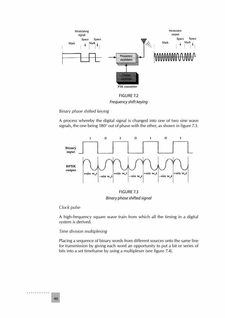
. . . . . . . . . . .46
FIGURE 7.2Frequency shift keying
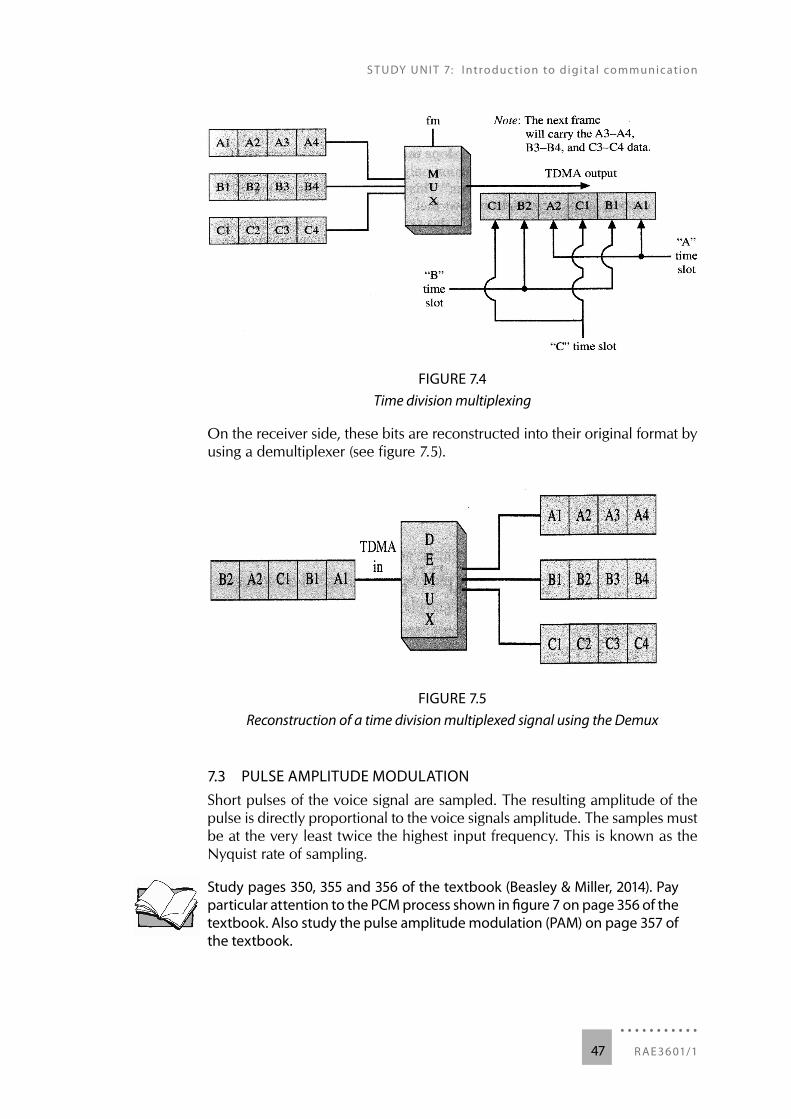
Binary phase shifted keying
A process whereby the digital signal is changed into one of two sine wave signals, the one being 180o out of phase with the other, as shown in figure 7.3.
FIGURE 7.3Binary phase shifted signal
Clock pulse
A high-frequency square wave train from which all the timing in a digital system is derived.
Time division multiplexing
Placing a sequence of binary words from different sources onto the same line for transmission by giving each word an opportunity to put a bit or series of bits into a set timeframe by using a multiplexer (see figure 7.4).
S T UDY UN I T 7: Intro du c t io n to digi t a l co mmunic at io n
. . . . . . . . . . .R AE 36 01/147
FIGURE 7.4Time division multiplexing
On the receiver side, these bits are reconstructed into their original format by using a demultiplexer (see figure 7.5).
FIGURE 7.5Reconstruction of a time division multiplexed signal using the Demux
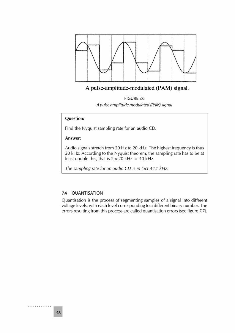
7.3 PULSE AMPLITUDE MODULATIONShort pulses of the voice signal are sampled. The resulting amplitude of the pulse is directly proportional to the voice signals amplitude. The samples must be at the very least twice the highest input frequency. This is known as the Nyquist rate of sampling.
Study pages 350, 355 and 356 of the textbook (Beasley & Miller, 2014). Pay particular attention to the PCM process shown in figure 7 on page 356 of the textbook. Also study the pulse amplitude modulation (PAM) on page 357 of the textbook.
. . . . . . . . . . .48
FIGURE 7.6A pulse amplitude modulated (PAM) signal
Question:
Find the Nyquist sampling rate for an audio CD.
Answer:
Audio signals stretch from 20 Hz to 20 kHz. The highest frequency is thus 20 kHz. According to the Nyquist theorem, the sampling rate has to be at least double this, that is 2 x 20 kHz = 40 kHz.
The sampling rate for an audio CD is in fact 44.1 kHz.
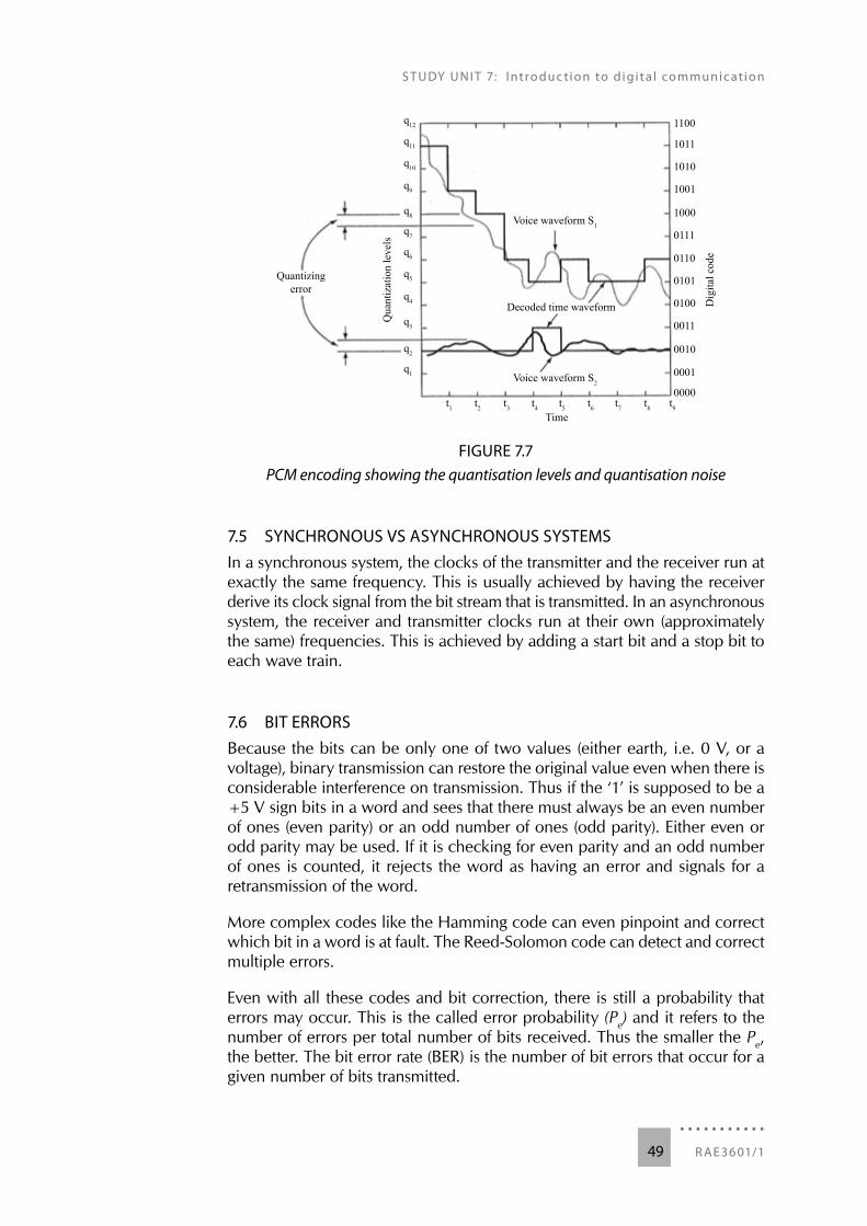
7.4 QUANTISATIONQuantisation is the process of segmenting samples of a signal into different voltage levels, with each level corresponding to a different binary number. The errors resulting from this process are called quantisation errors (see figure 7.7).
S T UDY UN I T 7: Intro du c t io n to digi t a l co mmunic at io n
. . . . . . . . . . .R AE 36 01/149
q12
q11
q10
q9
q8
q7
q6
q5
q4
q3
q2
q1
t1 t2 t3 t4 t5 t6 t7 t8 t9
1100
1011
1010
1001
1000
0111
0110
0101
0100
0011
0010
0001
0000
Quantizingerror
Qua
ntiz
atio
n le
vels
Dig
ital c
ode
Voice waveform S1
Voice waveform S2
Decoded time waveform
Time
FIGURE 7.7PCM encoding showing the quantisation levels and quantisation noise
7.5 SYNCHRONOUS VS ASYNCHRONOUS SYSTEMSIn a synchronous system, the clocks of the transmitter and the receiver run at exactly the same frequency. This is usually achieved by having the receiver derive its clock signal from the bit stream that is transmitted. In an asynchronous system, the receiver and transmitter clocks run at their own (approximately the same) frequencies. This is achieved by adding a start bit and a stop bit to each wave train.
7.6 BIT ERRORSBecause the bits can be only one of two values (either earth, i.e. 0 V, or a voltage), binary transmission can restore the original value even when there is considerable interference on transmission. Thus if the ‘1’ is supposed to be a +5 V sign bits in a word and sees that there must always be an even number of ones (even parity) or an odd number of ones (odd parity). Either even or odd parity may be used. If it is checking for even parity and an odd number of ones is counted, it rejects the word as having an error and signals for a retransmission of the word.
More complex codes like the Hamming code can even pinpoint and correct which bit in a word is at fault. The Reed-Solomon code can detect and correct multiple errors.
Even with all these codes and bit correction, there is still a probability that errors may occur. This is the called error probability (Pe) and it refers to the number of errors per total number of bits received. Thus the smaller the Pe, the better. The bit error rate (BER) is the number of bit errors that occur for a given number of bits transmitted.
. . . . . . . . . . .50
Question:
A transmission has a Pe of 10-5 and 108 bits are received. Calculate the BER and interpret the meaning of this figure.
Answer:
Average number of bits = m x Pe
= 108 x 10 -5
= 1 000
This means that for every 100 million bits that are received, about 1 000 errors can be expected.
7.7 QUESTIONS(1) Name FOUR ways in which a digital signal can be transmitted.(2) If an analogue signal that ranges from 100 Hz to 1 kHz is to be digitised,
what must the minimum sampling rate be?(3) Name THREE ways in which a digital signal can be checked for errors.(4) A transmission has an error probability of 10-5 and 107 bits are received.
Calculate the BER.
. . . . . . . . . . .R AE 36 01/151
8S T U D Y U N I T 8
8TRANSMISSION LINES AND CABLES
8.1 LEARNING OUTCOMESOnce you have completed this study unit, you should be able to do the following:
• Calculate the Z0 of the transmission, the velocity of propagation and the standing wave ratio (SWR) of lines.
• Describe the operational characteristics of twisted-pair cable and its testing considerations.
• Explain wave propagation and delay factors. • Describe the physical characteristics of transmission lines.
8.2 TYPES OF TRANSMISSION LINES
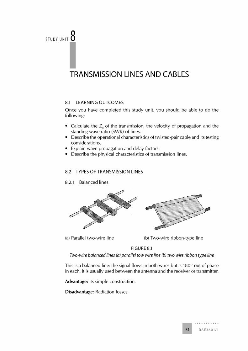
8.2.1 Balanced lines
(a) Parallel two-wire line (b) Two-wire ribbon-type line
FIGURE 8.1Two-wire balanced lines (a) parallel tow wire line (b) two wire ribbon type line
This is a balanced line: the signal flows in both wires but is 180° out of phase in each. It is usually used between the antenna and the receiver or transmitter.
Advantage: Its simple construction.
Disadvantage: Radiation losses.
. . . . . . . . . . .52
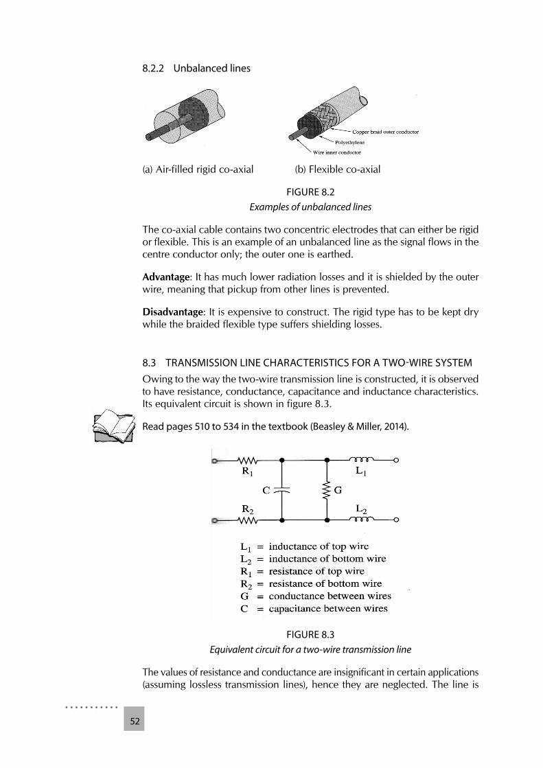
8.2.2 Unbalanced lines
(a) Air-filled rigid co-axial (b) Flexible co-axial
FIGURE 8.2Examples of unbalanced lines
The co-axial cable contains two concentric electrodes that can either be rigid or flexible. This is an example of an unbalanced line as the signal flows in the centre conductor only; the outer one is earthed.
Advantage: It has much lower radiation losses and it is shielded by the outer wire, meaning that pickup from other lines is prevented.
Disadvantage: It is expensive to construct. The rigid type has to be kept dry while the braided flexible type suffers shielding losses.
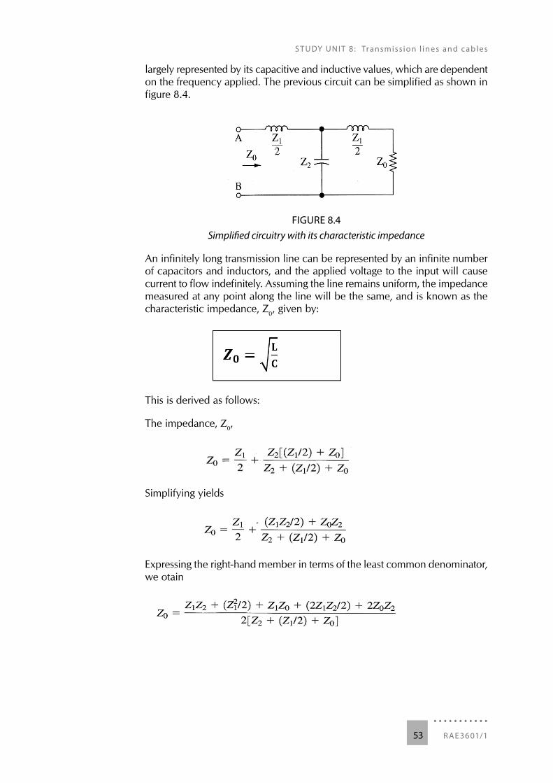
8.3 TRANSMISSION LINE CHARACTERISTICS FOR A TWO-WIRE SYSTEMOwing to the way the two-wire transmission line is constructed, it is observed to have resistance, conductance, capacitance and inductance characteristics. Its equivalent circuit is shown in figure 8.3.
Read pages 510 to 534 in the textbook (Beasley & Miller, 2014).
FIGURE 8.3Equivalent circuit for a two-wire transmission line
The values of resistance and conductance are insignificant in certain applications (assuming lossless transmission lines), hence they are neglected. The line is
S T UDY UN I T 8 : Tr ansmiss io n l in es an d c ab l es
. . . . . . . . . . .R AE 36 01/153
largely represented by its capacitive and inductive values, which are dependent on the frequency applied. The previous circuit can be simplified as shown in figure 8.4.
FIGURE 8.4Simplifi ed circuitry with its characteristic impedance
An infinitely long transmission line can be represented by an infinite number of capacitors and inductors, and the applied voltage to the input will cause current to flow indefinitely. Assuming the line remains uniform, the impedance measured at any point along the line will be the same, and is known as the characteristic impedance, Z0, given by:
This is derived as follows:
The impedance, Z0,
Simplifying yields
Expressing the right-hand member in terms of the least common denominator, we otain
. . . . . . . . . . .54
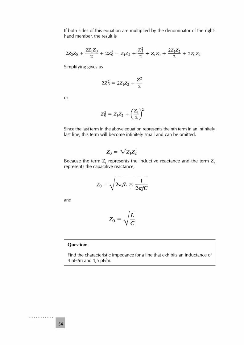
If both sides of this equation are multiplied by the denominator of the right-hand member, the result is
Simplifying gives us
or
Since the last term in the above equation represents the nth term in an infinitely last line, this term will become infinitely small and can be omitted.
Because the term Z1 represents the inductive reactance and the term Z2 represents the capacitive reactance,
and
Question:
Find the characteristic impedance for a line that exhibits an inductance of 4 nH/m and 1,5 pF/m.
S T UDY UN I T 8 : Tr ansmiss io n l in es an d c ab l es
. . . . . . . . . . .R AE 36 01/155
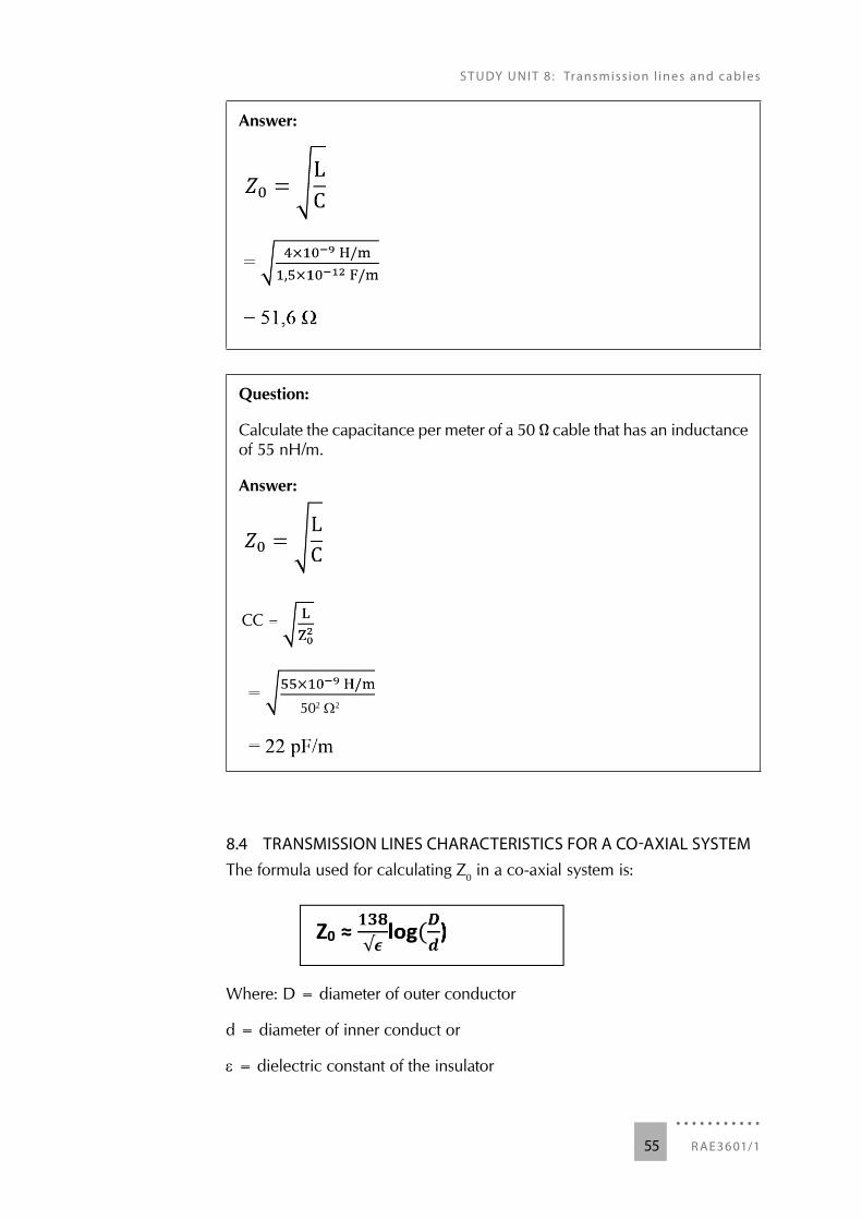
Answer:
Question:
Calculate the capacitance per meter of a 50 Ω cable that has an inductance of 55 nH/m.
Answer:
8.4 TRANSMISSION LINES CHARACTERISTICS FOR A CO-AXIAL SYSTEMThe formula used for calculating Z0 in a co-axial system is:
Where: D = diameter of outer conductor
d = diameter of inner conduct or
ε = dielectric constant of the insulator
CC
502 Ω2
. . . . . . . . . . .56
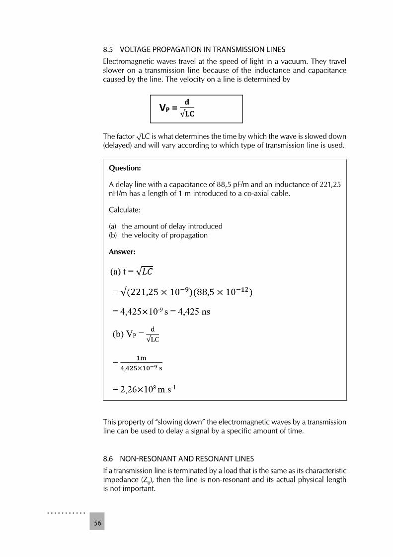
8.5 VOLTAGE PROPAGATION IN TRANSMISSION LINESElectromagnetic waves travel at the speed of light in a vacuum. They travel slower on a transmission line because of the inductance and capacitance caused by the line. The velocity on a line is determined by
The factor √LC is what determines the time by which the wave is slowed down (delayed) and will vary according to which type of transmission line is used.
Question:
A delay line with a capacitance of 88,5 pF/m and an inductance of 221,25 nH/m has a length of 1 m introduced to a co-axial cable.
Calculate:
(a) the amount of delay introduced (b) the velocity of propagation
Answer:
This property of “slowing down” the electromagnetic waves by a transmission line can be used to delay a signal by a specific amount of time.
8.6 NON-RESONANT AND RESONANT LINESIf a transmission line is terminated by a load that is the same as its characteristic impedance (Z0), then the line is non-resonant and its actual physical length is not important.
S T UDY UN I T 8 : Tr ansmiss io n l in es an d c ab l es
. . . . . . . . . . .R AE 36 01/157
If, however, a transmission line is not terminated by a load that is the same as its characteristic impedance (Z0), then the line is resonant and its actual physical length plays a vital role. Also, in a resonant line the termination of the line plays a role. This is because of the reflections that appear in a line. (A reflection is a reversal in direction of the voltage and current caused by the inductance and capacitance of the transmission line.)
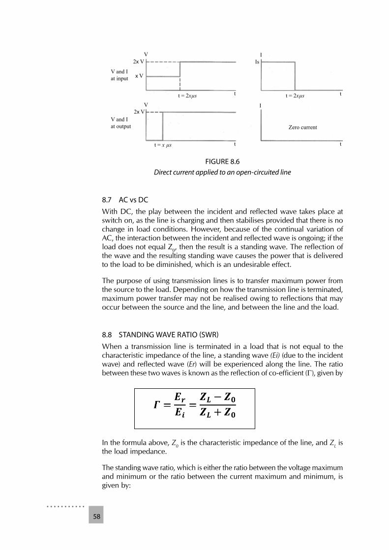
A voltage reflection from an open circuit is in phase, while the current reflection is out of phase. This means that the voltage reaches its full value at its load in the time that it takes the wave to travel to the load, but the voltage at the load only reaches its full value in the time it takes the wave to reach the load and be reflected back. Because the current is out of phase, it is always zero at the load, but the source experiences it for the time that it takes the wave to reach the load and the reflection to return.
The opposite happens if the line is terminated in a closed circuit. In other words, if the line is terminated in a short circuit, the voltage reflection is out of phase while the current reflection is in phase. This means that the current reaches its full value at its load in the time that it takes the wave to travel to the load, but the current at the load only reaches its full value in the time it takes for the wave to reach the load and be reflected back. Because the voltage is out of phase, it is always zero at the load, but the source experiences it for the time that it takes the wave to reach the load and the reflection to return.
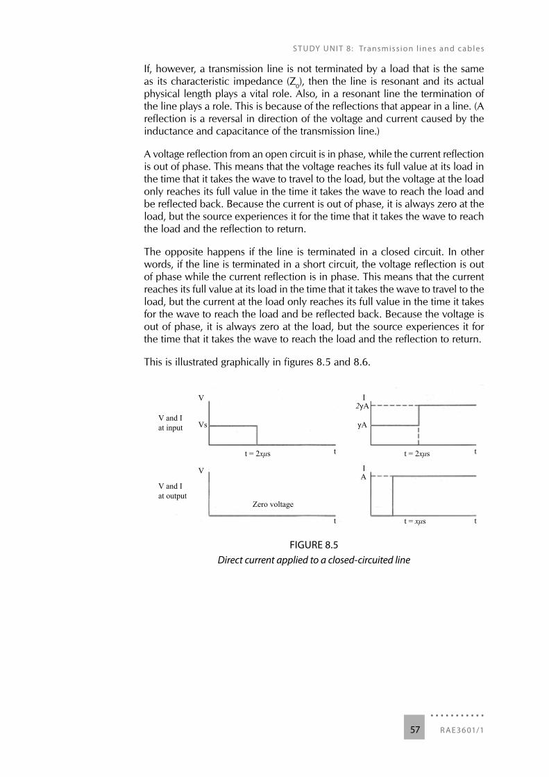
This is illustrated graphically in figures 8.5 and 8.6.
V and Iat input
V and Iat output
V
Vs
V
I
I
2yA
yA
A
t = 2xμst = 2xμs
t = xμs
Zero voltage
t
t
t
t
FIGURE 8.5Direct current applied to a closed-circuited line
. . . . . . . . . . .58
V and Iat input
V and Iat output
V2x V
x V
2x VV
t = 2xµs
t = x µs
t = 2xµs
Zero current
I
I
Is
t
t t
t
FIGURE 8.6Direct current applied to an open-circuited line
8.7 AC vs DCWith DC, the play between the incident and reflected wave takes place at switch on, as the line is charging and then stabilises provided that there is no change in load conditions. However, because of the continual variation of AC, the interaction between the incident and reflected wave is ongoing; if the load does not equal Z0, then the result is a standing wave. The reflection of the wave and the resulting standing wave causes the power that is delivered to the load to be diminished, which is an undesirable effect.
The purpose of using transmission lines is to transfer maximum power from the source to the load. Depending on how the transmission line is terminated, maximum power transfer may not be realised owing to reflections that may occur between the source and the line, and between the line and the load.
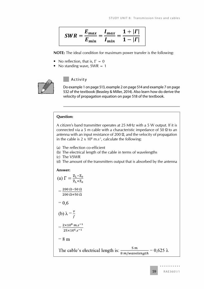
8.8 STANDING WAVE RATIO (SWR)When a transmission line is terminated in a load that is not equal to the characteristic impedance of the line, a standing wave (Ei) (due to the incident wave) and reflected wave (Er) will be experienced along the line. The ratio between these two waves is known as the reflection of co-efficient (Γ), given by
In the formula above, Z0 is the characteristic impedance of the line, and ZL is the load impedance.
The standing wave ratio, which is either the ratio between the voltage maximum and minimum or the ratio between the current maximum and minimum, is given by:
S T UDY UN I T 8 : Tr ansmiss io n l in es an d c ab l es
. . . . . . . . . . .R AE 36 01/159
NOTE: The ideal condition for maximum power transfer is the following:
• No refl ection, that is, Γ = 0 • No standing wave, SWR = 1
7Ac tiv it y
Do example 1 on page 513, example 2 on page 514 and example 7 on page 532 of the textbook (Beasley & Miller, 2014). Also learn how do derive the velocity of propagation equation on page 518 of the textbook.
Question:
A citizen’s band transmitter operates at 25 MHz with a 5 W output. If it is connected via a 5 m cable with a characteristic impedance of 50 Ω to an antenna with an input resistance of 200 Ω, and the velocity of propagation in the cable is 2 x 10⁸ m.s-1, calculate the following:
(a) The refl ection co-effi cient (b) The electrical length of the cable in terms of wavelengths (c) The VSWR (d) The amount of the transmitters output that is absorbed by the antenna
Answer:
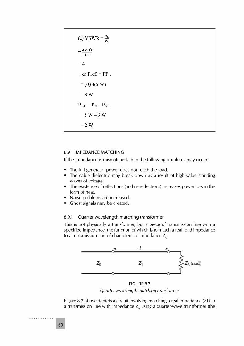
. . . . . . . . . . .60
8.9 IMPEDANCE MATCHINGIf the impedance is mismatched, then the following problems may occur:
• The full generator power does not reach the load. • The cable dielectric may break down as a result of high-value standing
waves of voltage. • The existence of refl ections (and re-refl ections) increases power loss in the
form of heat. • Noise problems are increased. • Ghost signals may be created.
8.9.1 Quarter wavelength matching transformerThis is not physically a transformer, but a piece of transmission line with a specified impedance, the function of which is to match a real load impedance to a transmission line of characteristic impedance Z0.
FIGURE 8.7Quarter wavelength matching transformer
Figure 8.7 above depicts a circuit involving matching a real impedance (ZL) to a transmission line with impedance Z0 using a quarter-wave transformer (the
S T UDY UN I T 8 : Tr ansmiss io n l in es an d c ab l es
. . . . . . . . . . .R AE 36 01/161
section of the line l). The characteristic impedance of the transformer at the design frequency f0 is given by
What should be the approximate surge impedance of a quarter-wavelength matching line used to match a 600 Ω feeder to a 70 Ω (resistive) antenna?
8.9.2 Single-stub tuningA single-stub tuning technique uses either an open-circuited or a short-circuited transmission line, inserted in series or in parallel with the main transmission feedline at a specific distance from the load. In designing a single-stub tuning circuit, the most important parameters are the distance, d, from the load to where the stub will be inserted, and the value of susceptance or reactance that would be provided by the stub. The distance, d, from the load is dependent on the operating frequency and load impedance.
• Series connection. The distance, d, is selected so that the impedance, Z, seen looking into the line at a distance d from the load is of the form Z0 + jX. Then the stub reactance is chosen as −jX, resulting in a matched condition.
• Parallel/Shunt connection. Select d so that the admittance, Y, seen looking into the line at distance d from the load is of the form Y0 + jB. Then the stub susceptance is chosen as −jB, resulting in a matched condition.
• Shunt stubs are preferred for microstrip lines or striplines, while series stubs are preferred for slotlines or coplanar waveguides.
8.10 TRANSMISSION LINE APPLICATIONS
8.10.1 Discrete circuit simulationTransmission lines can be used to simulate passive components, such as inductors and capacitors (or combinations of the two, such as LC resonating circuits).
8.10.2 BalunsThis is a transformer that connects a balanced load (e.g. an antenna) to an unbalanced load (e.g. a co-axial cable) (See figure 8.8). A transmission line, like the one shown in figure 8.8, can replace a physical transformer so that excessive losses that occur in a transformer with high frequencies are eliminated.

. . . . . . . . . . .62
UnbalancedP
Balanced
B
A
FIGURE 8.8Baluns
8.10.3 FiltersA quarter-wave section of a transmission line can be used to filter out the even harmonics.
8.10.4 Slotted linesA length-wise slot cut in the outer conductor of a co-axial cable with a pick-up probe can be used as a measuring instrument to find the magnitude of the signal accurately so that the voltage standing wave ratio, the generator frequency and the load impedance can be determined.
8.10.5 Time-domain reflectometryA pulse sent down a transmission line has the duration to its reflection measured. This can give a very accurate indication (to within a metre of a 16 km line) of where the break in a line is. If no reflection is found, it indicates perfectly matched load.
8.11 QUESTIONS(1) An SSB transmitter at 2,27 MHz and 200 W output is connected to an
antenna, Rin = 150 Ω, via 75 m of RG-8A/U cable. (RG-8A/U cable has a capacitance of 96,785 pF/m and 241,962 nH/m).
Determine:
(a) The reflection coefficient(b) The electrical cable length in wavelengths(c) The SWR(d) The amount of power absorbed by the antenna
(2) Name and describe the construction and advantages of TWO types of transmission lines.
S T UDY UN I T 8 : Tr ansmiss io n l in es an d c ab l es
. . . . . . . . . . .R AE 36 01/163
(3) Find the characteristic impedance for a line that exhibits an inductance of 6 nH/m and 2,5 pF/m.
(4) What is the difference between a resonant line and a non-resonant line?
. . . . . . . . . . .64
9S T U D Y U N I T 9
9RADIO WAVE PROPAGATION
9.1 LEARNING OUTCOMESOnce you have completed this study unit, you should be able to do the following:
• Describe the structure of electromagnetic waves, and explain wave reflection, wave refraction and wave diffraction.
• Explain ground-wave propagation and space-wave propagation, and perform calculations relating to radio wave propagation.
9.2 ELECTROMAGNETIC WAVES
9.2.1 Electrical to electromagnetic conversionA transmitting antenna is a transducer that converts electrical energy into electromagnetic energy. A receiving antenna is a transducer that converts electromagnetic energy back into electrical energy.
9.2.2 Electromagnetic wavesThe transmitted wave moves away at 90° from the transmitting antenna. It consists of an electrical field and a magnetic field at 90° to each other, as shown in figure 9.1. It is said to be polarised in the plane of the electric field.
Study pages 562 to 569 of the textbook (Beasley & Miller, 2014).
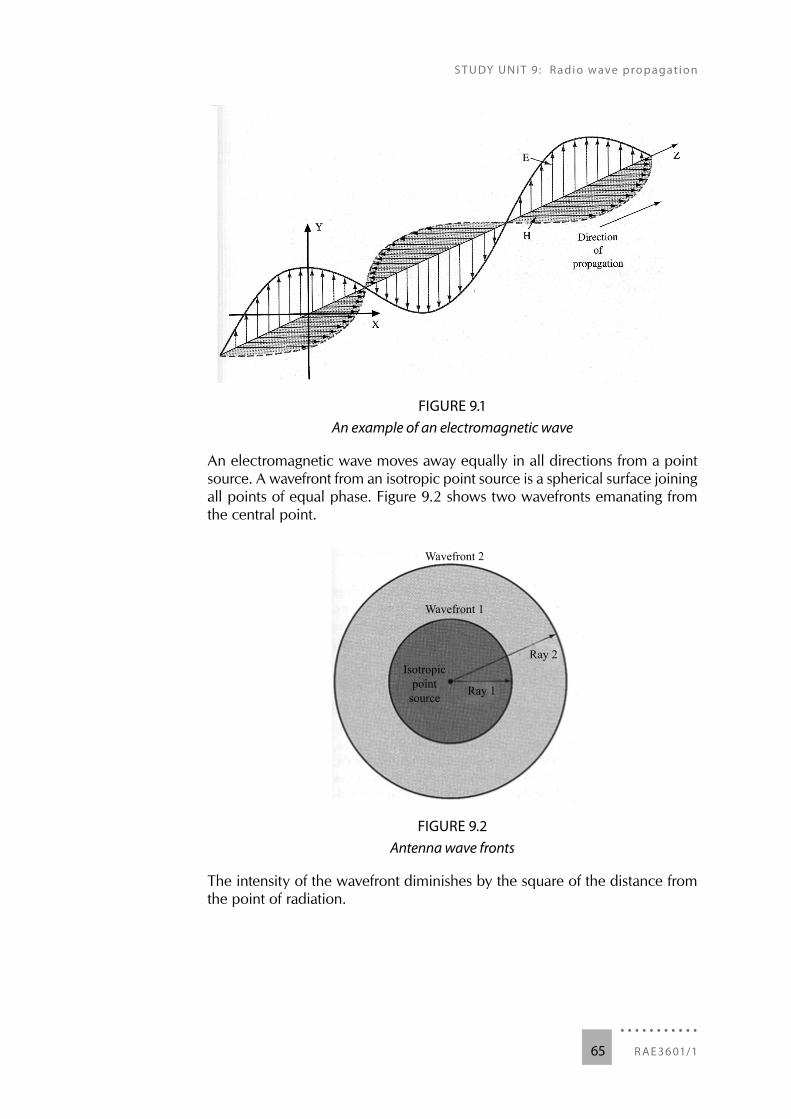
S T UDY UN I T 9 : R adio w ave p ro p agat io n
. . . . . . . . . . .R AE 36 01/165
FIGURE 9.1An example of an electromagnetic wave
An electromagnetic wave moves away equally in all directions from a point source. A wavefront from an isotropic point source is a spherical surface joining all points of equal phase. Figure 9.2 shows two wavefronts emanating from the central point.
Wavefront 2
Wavefront 1
Isotropicpoint
source Ray 1
Ray 2
FIGURE 9.2Antenna wave fronts
The intensity of the wavefront diminishes by the square of the distance from the point of radiation.
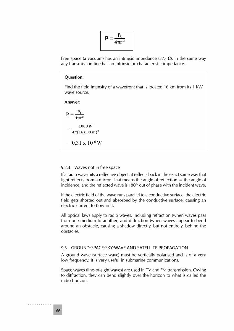
. . . . . . . . . . .66
Free space (a vacuum) has an intrinsic impedance (377 Ω), in the same way any transmission line has an intrinsic or characteristic impedance.
Question:
Find the field intensity of a wavefront that is located 16 km from its 1 kW wave source.
Answer:
9.2.3 Waves not in free spaceIf a radio wave hits a reflective object, it reflects back in the exact same way that light reflects from a mirror. That means the angle of reflection = the angle of incidence; and the reflected wave is 180° out of phase with the incident wave.
If the electric field of the wave runs parallel to a conductive surface, the electric field gets shorted out and absorbed by the conductive surface, causing an electric current to flow in it.
All optical laws apply to radio waves, including refraction (when waves pass from one medium to another) and diffraction (when waves appear to bend around an obstacle, causing a shadow directly, but not entirely, behind the obstacle).
9.3 GROUND-SPACE-SKY-WAVE AND SATELLITE PROPAGATIONA ground wave (surface wave) must be vertically polarised and is of a very low frequency. It is very useful in submarine communications.
Space waves (line-of-sight waves) are used in TV and FM transmission. Owing to diffraction, they can bend slightly over the horizon to what is called the radio horizon.

S T UDY UN I T 9 : R a dio w ave p ro p agat io n
. . . . . . . . . . .R AE 36 01/167
This can be calculated as follows:
In this formula, ht and hr are the heights of the receiving antennas.
Question:
An 83.82 metre high transmitting antenna has a receiving antenna which is 18.288 metres high and has a gain of 3 dB. The transmitter power is 100 W at 224 MHz. Calculate the maximum transmitting distance.
Answer:
Sky-wave propagation is radiated towards the ionosphere, where it is refracted back to the earth and reflected back up to the sky in an action called skipping. The distance between skips is called the quiet or skip zones, as reception is not possible. Because of the continually changing shape of the ionosphere (day/night, summer/winter and solar flares all influence its nature and height), the reception path is not always predictable.
Satellite communications involve having a ground station with a highly directional transmitting antenna sending a high-frequency signal through the ionosphere to the satellite that acts as a transponder, that is it performs as a receiver, frequency translator and then as a re-transmitter (at a different frequency from the received signal) back to earth.
One satellite typically allows communication among several users through multiplexing. This used to be possible mainly as the result of frequency-division multiple-access, but it is now possible via time-division multiple-access and code-division multiple-access.
8Ac tiv it y
Work through example 1 on page 570 of the textbook (Beasley & Miller, 2014).
. . . . . . . . . . .68
9.4 QUESTIONS(1) Calculate the field intensity 20 km from a 2 kW source.(2) What is diffraction of electromagnetic waves? Explain the significance of
the shadow zone and how it is created.(3) Describe ground-wave propagation and attenuation in detail.(4) Describe how the layers in the ionosphere are affected in a 24-hour period.
. . . . . . . . . . .R AE 36 01/169
10S T U D Y U N I T 1 0
10ANTENNA THEORY
10.1 LEARNING OUTCOMESOnce you have completed this study unit, you should be able to do the following:
• Explain the transmission line theory and the development of the half-wave dipole antenna.
• Define antenna reciprocity and polarisation. • Explain antenna radiation and induction fields, radiation patterns, gains
and radiation resistance. • Explain and calculate antenna efficiency. • Describe common antenna types and arrays. • Explain and differentiate between antenna beam width and bandwidth.
Any antenna can be used as a receiving or a transmitting antenna, which means that it can transfer electromagnetic waves from the atmosphere into electrical signals as efficiently as it can transfer electrical signals into electromagnetic waves. This property is known as reciprocity.
Polarisation refers to the orientation of the electric field in an electromagnetic wave. For best reception, the receiving antenna must have the same polarisation as the transmitting antenna.
Study pages 610 to 634 in the textbook (Beasley & Miller, 2014).
10.2 HALF-WAVE DIPOLE ANTENNAAn antenna that has a physical length that is half the wavelength of the applied frequency is called a half-wave dipole antenna (λ/2 dipole). These antennas are made for frequencies upwards of about 2 MHz. Any lower frequency with this configuration would require an antenna that is impractically large.
The λ/2 dipole is constructed by “folding out” a quarter-wave dipole (λ/4 dipole), as is illustrated in figures 10.1 and 10.2. The impedance of this antenna varies from 73 Ω where the source is connected to about 2,5 kΩ at the open ends. This is also illustrated in figures 10.1 and 10.2.
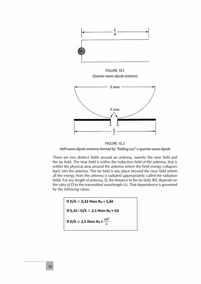
. . . . . . . . . . .70
FIGURE 10.1Quarter-wave dipole antenna
FIGURE 10.2Half-wave dipole antenna formed by “folding out” a quarter-wave dipole
There are two distinct fields around an antenna, namely the near field and the far field. The near field is within the induction field of the antenna, that is within the physical area around the antenna where the field energy collapses back into the antenna. The far field is any place beyond the near field where all the energy from the antenna is radiated (appropriately called the radiation field). For any length of antenna, D, the distance to the far field, Rff, depends on the ratio of D to the transmitted wavelength (λ). That dependence is governed by the following ratios:
S T UDY UN I T 10 : Antenna th e o r y
. . . . . . . . . . .R AE 36 01/171
Question:
Determine where the far field would begin for a λ/2 dipole that has been designed to transmit a 200 MHz signal.
Answer:
Wavelength for a 200 MHz signal is given as:
For a λ/2 dipole, D = λ/2 = 1,5 m/2 = 0,75 m.
Thus choose equation: Rff = 5 D = 5(0,75 m) = 3,75 m.
Hence the far field (radiation field) starts 3,75 m away from the antenna.
10.3 ANTENNA GAINAntenna gain is not the same as amplifier gain. Amplifier gain tells us by how much a signal is increased or boosted. An antenna does not boost a signal – it radiates (at best) a power value that is equal to the input power. Antenna gain refers to the ratio by which an antenna radiates better than another type of antenna with the same input power. A λ/2 dipole has a gain of 2,15 dB in comparison with an isotropic antenna. This gain is then measured in dBi. When other antennas are compared to λ/2 dipoles, this is indicated by dBd. Thus all λ/2 dipoles have a gain of 2,15 dBi (when compared to an isotropic antenna) and a gain of 1 dBd (when compared to other λ/2 dipoles).
If an antenna has a gain of 5 dBd, it means its gain is 5 dB greater than that of a λ/2 dipole, and 7,15 dB greater than an isotropic antenna (5 dB + 2,15 dB).
The amount of power received by an antenna is:
where G is the gain of the respective antennas and d is the distance between them.
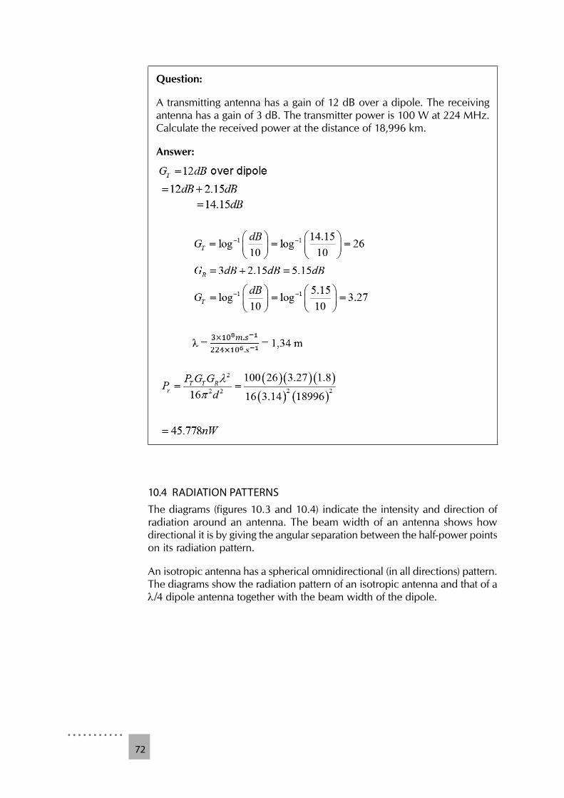
. . . . . . . . . . .72
Question:
A transmitting antenna has a gain of 12 dB over a dipole. The receiving antenna has a gain of 3 dB. The transmitter power is 100 W at 224 MHz. Calculate the received power at the distance of 18,996 km.
Answer:
10.4 RADIATION PATTERNSThe diagrams (figures 10.3 and 10.4) indicate the intensity and direction of radiation around an antenna. The beam width of an antenna shows how directional it is by giving the angular separation between the half-power points on its radiation pattern.
An isotropic antenna has a spherical omnidirectional (in all directions) pattern. The diagrams show the radiation pattern of an isotropic antenna and that of a λ/4 dipole antenna together with the beam width of the dipole.
S T UDY UN I T 10 : Antenna th e o r y
. . . . . . . . . . .R AE 36 01/173
FIGURE 10.3Isotropic point radiation pattern
FIGURE 10.4λ/4 dipole radiation pattern
It must be noted that all radiation patterns represent three-dimensional (3D) phenomena in two dimensions. The following figure shows a 3D representation of the radiation pattern around a λ/2 dipole antenna.
FIGURE 10.5Three-dimensional antenna radiation pattern for a λ/2 dipole
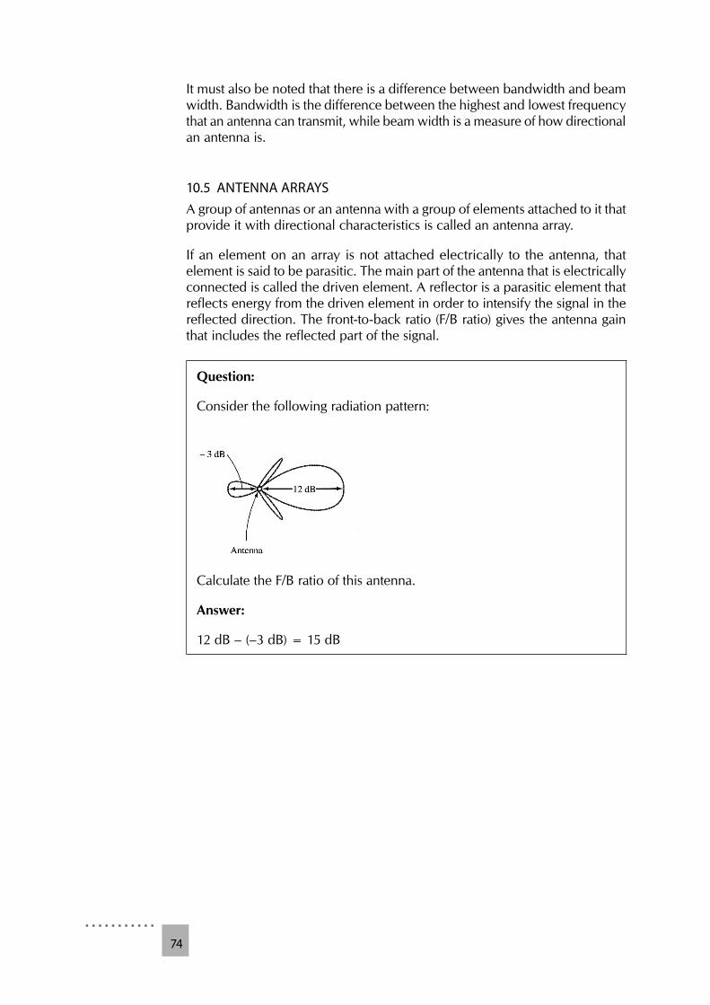
. . . . . . . . . . .74
It must also be noted that there is a difference between bandwidth and beam width. Bandwidth is the difference between the highest and lowest frequency that an antenna can transmit, while beam width is a measure of how directional an antenna is.
10.5 ANTENNA ARRAYSA group of antennas or an antenna with a group of elements attached to it that provide it with directional characteristics is called an antenna array.
If an element on an array is not attached electrically to the antenna, that element is said to be parasitic. The main part of the antenna that is electrically connected is called the driven element. A reflector is a parasitic element that reflects energy from the driven element in order to intensify the signal in the reflected direction. The front-to-back ratio (F/B ratio) gives the antenna gain that includes the reflected part of the signal.
Question:
Consider the following radiation pattern:
Calculate the F/B ratio of this antenna.
Answer:
12 dB – (–3 dB) = 15 dB
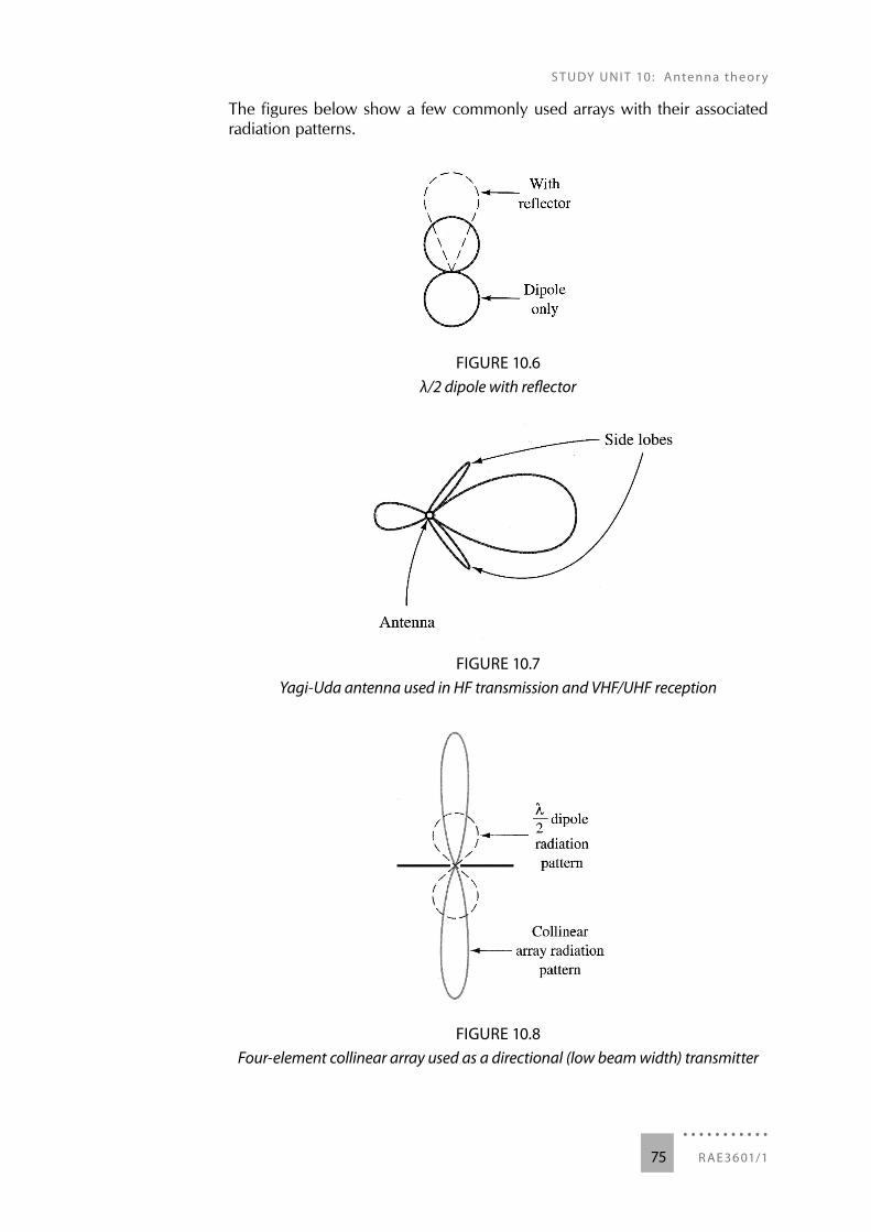
S T UDY UN I T 10 : Antenna th e o r y
. . . . . . . . . . .R AE 36 01/175
The figures below show a few commonly used arrays with their associated radiation patterns.
FIGURE 10.6λ/2 dipole with reflector
FIGURE 10.7Yagi-Uda antenna used in HF transmission and VHF/UHF reception
FIGURE 10.8Four-element collinear array used as a directional (low beam width) transmitter
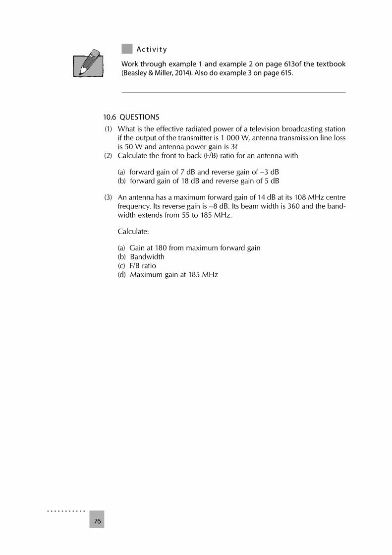
. . . . . . . . . . .76
9Ac tiv it y
Work through example 1 and example 2 on page 613of the textbook (Beasley & Miller, 2014). Also do example 3 on page 615.
10.6 QUESTIONS(1) What is the effective radiated power of a television broadcasting station
if the output of the transmitter is 1 000 W, antenna transmission line loss is 50 W and antenna power gain is 3?
(2) Calculate the front to back (F/B) ratio for an antenna with
(a) forward gain of 7 dB and reverse gain of –3 dB(b) forward gain of 18 dB and reverse gain of 5 dB
(3) An antenna has a maximum forward gain of 14 dB at its 108 MHz centre frequency. Its reverse gain is –8 dB. Its beam width is 360 and the band-width extends from 55 to 185 MHz.
Calculate:
(a) Gain at 180 from maximum forward gain(b) Bandwidth (c) F/B ratio(d) Maximum gain at 185 MHz