Radio Frequency Filters
27
Radio Frequency Filters Material courtesy of Fikret Dülger, Texas A&M University Electrical and Computer Engineering Department Analog & Mixed-Signal Design Center ECEN 665 (ESS)
Transcript of Radio Frequency Filters
Radio Frequency Filters
Material courtesy of Fikret Dülger,
Texas A&M UniversityElectrical and Computer Engineering Department
Analog & Mixed-Signal Design Center
ECEN 665 (ESS)

2
Outline
Problem Definition, Motivations and Research Goal
A Fully-Integrated Q-Enhancement LC Bandpass Filter
Noise AnalysisNonlinearity AnalysisIC Measurements of the Filter in 0.35μm CMOS
Comparison with previous reported filters and Conclusions
3
Problem Definition and Motivations
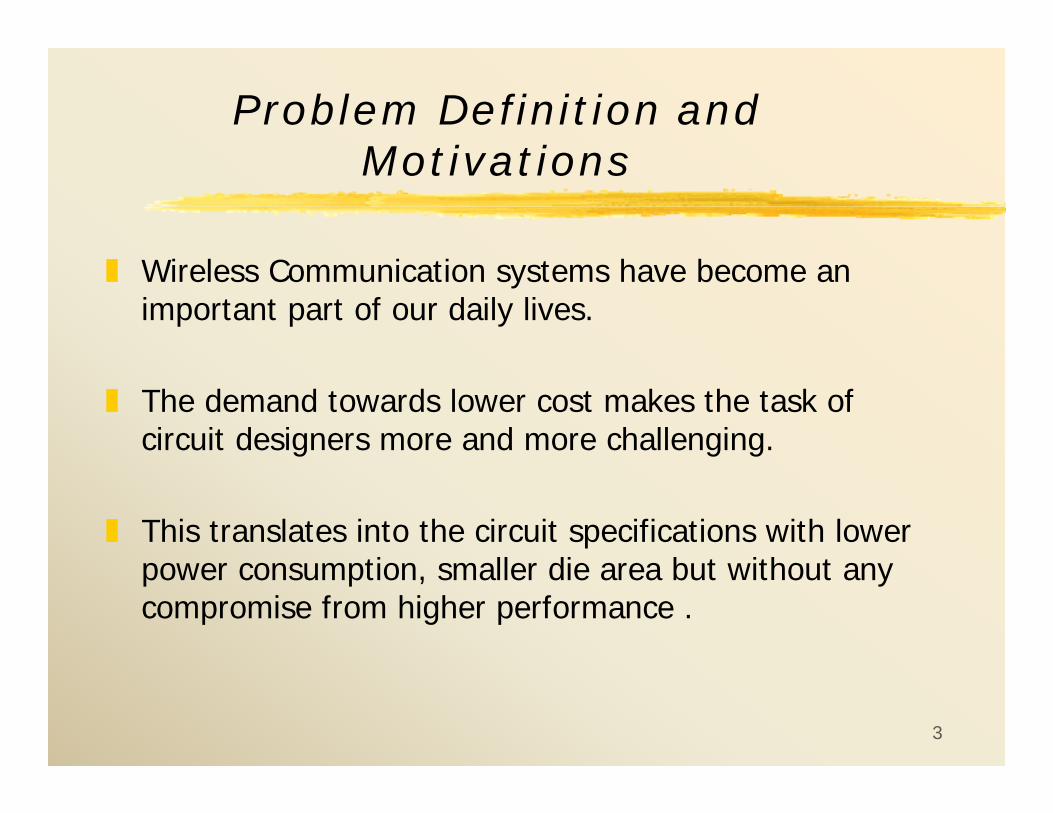
Wireless Communication systems have become an important part of our daily lives.
The demand towards lower cost makes the task of circuit designers more and more challenging.
This translates into the circuit specifications with lower power consumption, smaller die area but without any compromise from higher performance .
4
Problem Definition and Motivations
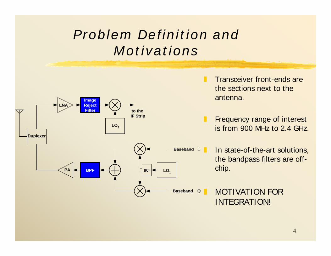
Transceiver front-ends are the sections next to the antenna.
Frequency range of interest is from 900 MHz to 2.4 GHz.
In state-of-the-art solutions, the bandpass filters are off-chip.
MOTIVATION FOR INTEGRATION!
to the IF Strip
ImageRejectFilter
LNA
BPFPA
Duplexer
90o
Baseband I
Baseband Q
LO2
LO1
5
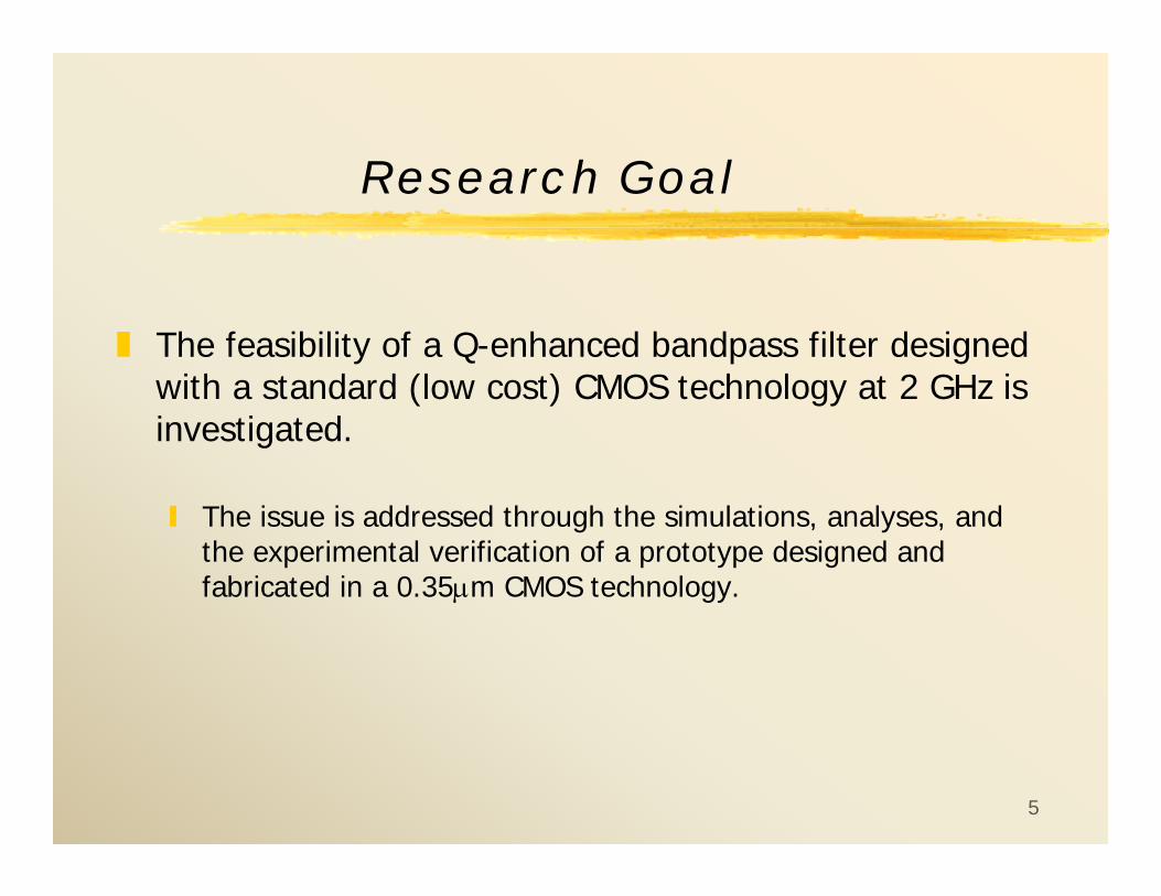
Research Goal
The feasibility of a Q-enhanced bandpass filter designed with a standard (low cost) CMOS technology at 2 GHz is investigated.
The issue is addressed through the simulations, analyses, and the experimental verification of a prototype designed and fabricated in a 0.35μm CMOS technology.
6
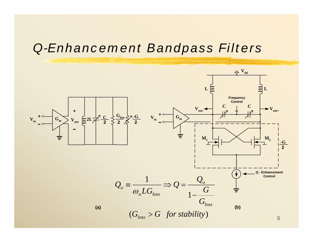
Q-Enhancement Bandpass Filters
GmVin+
Q - EnhancementControl
M1 M2
Vout- Vout+
L
C C
L
Vdd
-G
GmVin+-G2L C Gloss
2Vout
+
(b)(a)
FrequencyControl
2 2
2
)(
1
1
stabilityforGGGG
QQLG
Q
loss
loss
o
lossoo
>
−=⇒≡
ω
7
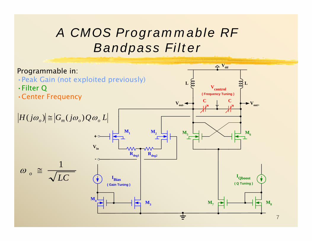
A CMOS Programmable RF Bandpass Filter
Programmable in:•Peak Gain (not exploited previously)•Filter Q•Center Frequency
LQjGjH oomo ωωω )()( ≅
LCo1
≅ω
M5 M6
Vcontrol
Vout- Vout+
L
C C
L
Vdd
Rdeg1 Rdeg2
M1 M2
Vin
+
-
M7 M8
IQboost
M3
M4
IBias( Q Tuning )
( Frequency Tuning )
( Gain Tuning )

8
A CMOS Programmable BandpassFilter
The peak gain programmability through the input Gmstage.
Increasing Q also increases the peak gain.
If ωοand Q are fixed, the peak gain can be modified through Gm.
LQjGGG
jGjH oomloss
omo ωωωω )()()( =
−≅
9
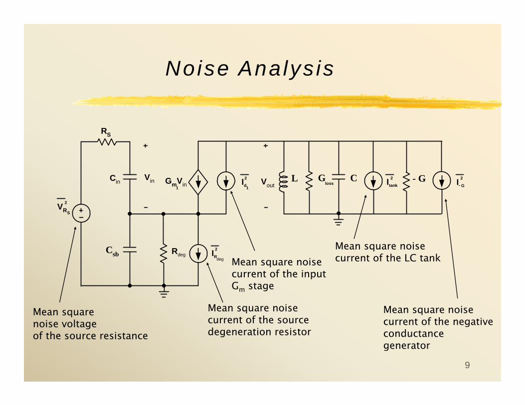
Noise Analysis
GmVin1
Vin
RS
Cin L Gloss
- GItank
2 I G
2Vout
Rdeg
C
Csb IR
2
deg
2Id1
VR2
S
Mean squarenoise voltageof the source resistance
Mean square noise current of the source degeneration resistor
Mean square noise current of the input Gm stage
Mean square noise current of the LC tank
Mean square noise current of the negative conductancegenerator

10
Noise Analysis (contd.)
The noise factor at ωo is obtained as
The calculations yield the following percentage contributions from the components:
Increasing Gm reduces the contribution of -G and the LC tank
21
2
2
221
22
42
4
)(2281 deg
mS
d
mS
oSmRGloss
GkTRI
GkTR
jZGIIkTGF inin +
+++= − ω
LC Tank: 44.5%, -G: 38%, Input Gm: 13.5%, Rdeg: 2.7%

11
Nonlinearity Analysis
There are three main nonlinearity contributors:
the negative conductance generatorthe varactorthe input Gm stage
The analyses consider each contributor separately!
Isolating each contributor allows us to identify the design trade-offs involved.
12
Nonlinearity Analysis (contd.)
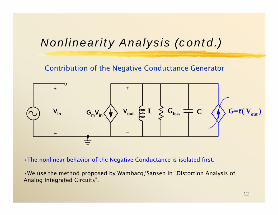
•The nonlinear behavior of the Negative Conductance is isolated first.
•We use the method proposed by Wambacq/Sansen in “Distortion Analysis of Analog Integrated Circuits”.
Contribution of the Negative Conductance Generator
GmVinVin L CGloss G=f( Vout )Vout

13
Noise-linearity, Q-selectivity-linearity trade-offs !
The 1dB compression point is approximated as:
The effective bias of the negative conductance should be maximized With a higher Qo, a lower gm5 is required: higher eff. bias with given Iss. The higher the peak gain, GmQωoL, the worse the linearity.
( )⎟⎟⎠
⎞⎜⎜⎝
⎛
⎟⎟⎠
⎞⎜⎜⎝
⎛−+
+
×≅ 3332
555
5222
11
12
32.2
5
5
LQGVV
gKK
gV
om
TGS
m
mdB ω
θθ
( )( ) ⎟⎟⎠
⎞⎜⎜⎝
⎛
−+⎟⎟⎠
⎞⎜⎜⎝
⎛≅ 3
555
52 1
12 TGS
OXo
VVLWCK
θμ
14
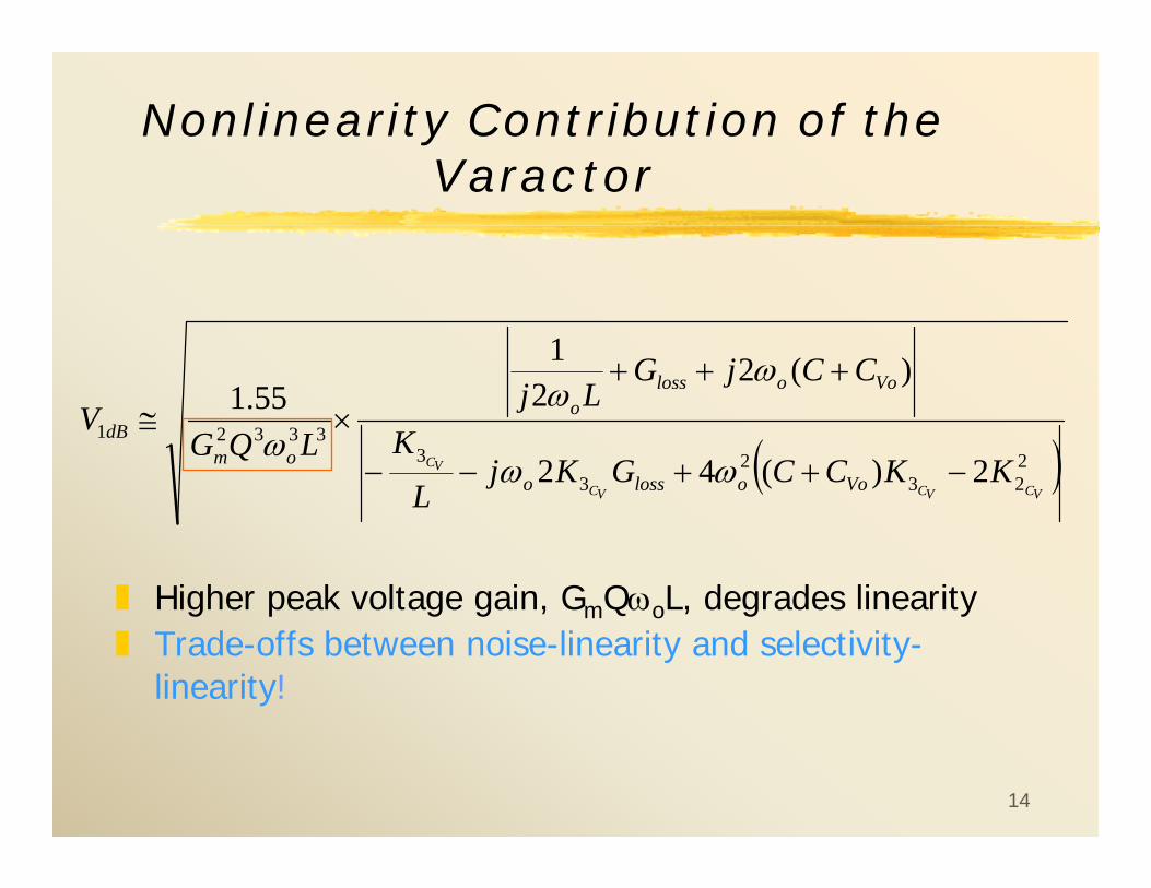
Nonlinearity Contribution of the Varactor
Higher peak voltage gain, GmQωoL, degrades linearityTrade-offs between noise-linearity and selectivity-linearity!
( )223
23
333321
2)(42
)(22
155.1
VCVCVC
VC KKCCGKjL
K
CCjGLj
LQGV
Voolosso
Voolosso
omdB
−++−−
+++×≅
ωω
ωω
ω

15
The effective bias of the transistors should be maximized!Increasing Rdeg improves the linearity with a penalty in power consumption for the same input Gm. The same applies to adding Rdeg to the cross-coupled pair
linearity-power trade-off
⎟⎟⎠
⎞⎜⎜⎝
⎛
−++
+×≅
)(12
)1(32.2
111
11222
3deg1
21
1
1
1TGS
mG
mmdB
VVGK
K
RGGV
mG
m θ
θ
Nonlinearity Contribution of the Input Gm stage
16
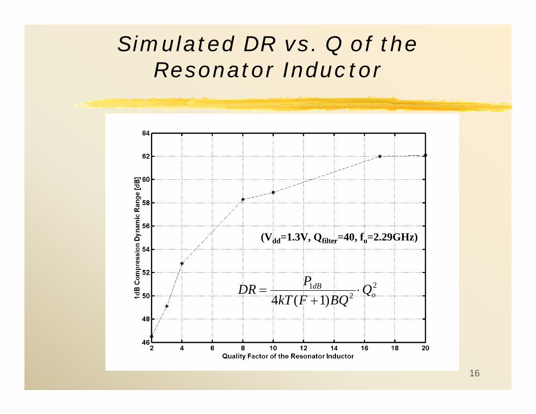
Simulated DR vs. Q of the Resonator Inductor
(Vdd=1.3V, Qfilter=40, fo=2.29GHz)
22
1
)1(4 odB Q
BQFkTPDR ⋅+
=

17
Dynamic Range Simulations

18
Integrated Circuit Measurements
TSMC 0.35μm CMOS technology
The second poly was not used. Compatibility with a standard Digital CMOS
The filter operates with a supply voltage of 1.3V, and 4mA for a Q= 40 at 2.19GHz
Chip area+buffers~ 0.1mm2.

19
Measured Q-Tuning
Q~170
Q~20
More than 3 octaves at fo=2.16GHz
5dB/div
30M
Hz
20
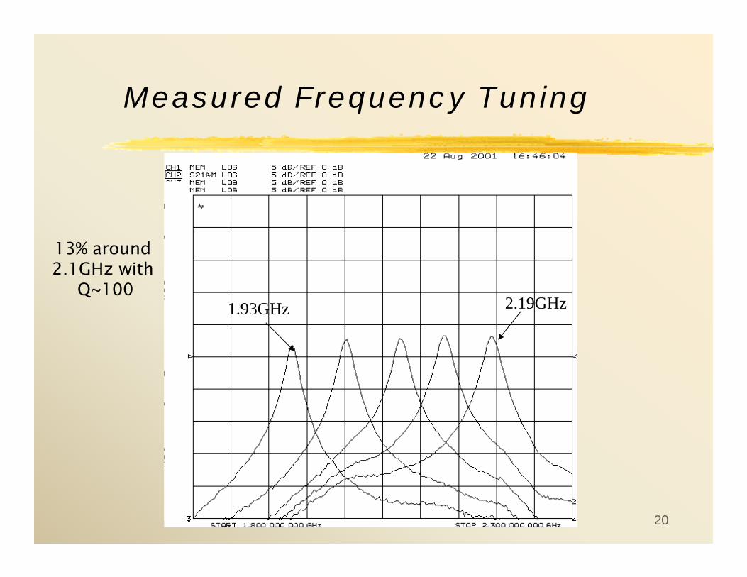
Measured Frequency Tuning
1.93GHz 2.19GHz
13% around 2.1GHz with
Q~100
21
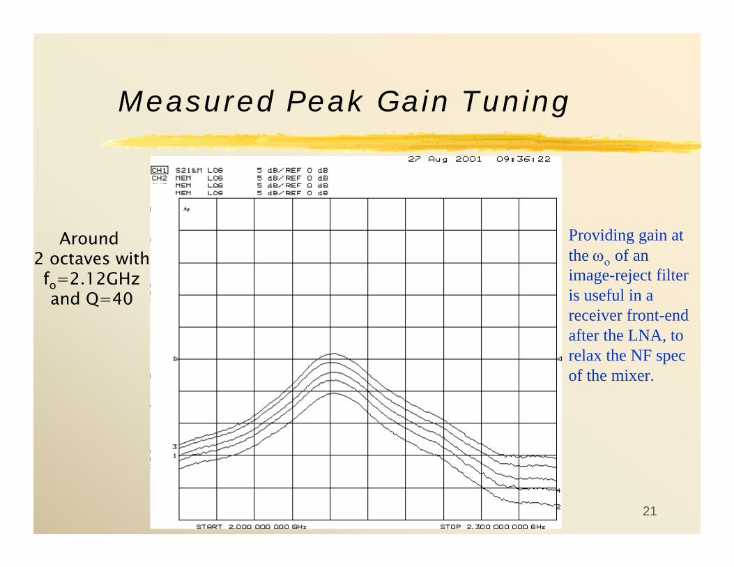
Measured Peak Gain Tuning
Around 2 octaves withfo=2.12GHzand Q=40
Providing gain at the ωο of an image-reject filter is useful in a receiver front-end after the LNA, to relax the NF spec of the mixer.

22
Overlaid Measurements of 10 different ICs
(a) with the same bias settings
(b) programmed for the same fo, gain and Q=40
Q : 20-80
fo : 2.14-2.18GHz
23
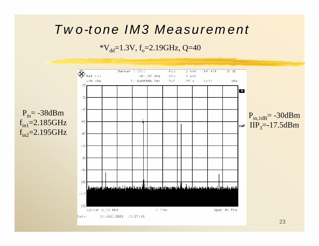
Two-tone IM3 Measurement
Pin= -38dBmfin1=2.185GHzfin2=2.195GHz
*Vdd=1.3V, fo=2.19GHz, Q=40
Pin,1dB= -30dBmIIP3=-17.5dBm

24
1 dB Compression Comparison
simulation
measurement
*Vdd=1.5V, fo=2.17GHz
25
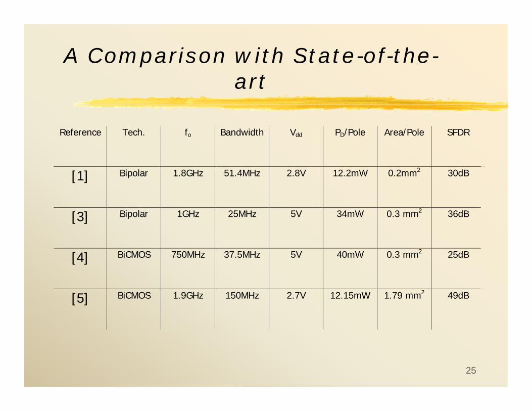
A Comparison with State-of-the-art
Reference Tech. fo Bandwidth Vdd PD/Pole Area/Pole SFDR
[1] Bipolar 1.8GHz 51.4MHz 2.8V 12.2mW 0.2mm2 30dB
[3] Bipolar 1GHz 25MHz 5V 34mW 0.3 mm2 36dB
[4] BiCMOS 750MHz 37.5MHz 5V 40mW 0.3 mm2 25dB
[5] BiCMOS 1.9GHz 150MHz 2.7V 12.15mW 1.79 mm2 49dB

26
A Comparison with State-of-the-art (contd.)
Reference Tech. fo Bandwidth Vdd PD/Pole Area/Pole SFDR
[2] CMOS 850MHz 18MHz 2.7V 52mW 0.5mm2 55dB
[6] CMOS 850MHz 28.3MHz 2V 22.9mW 0.32mm2 28dB
[7] CMOS 2.14GHz 60MHz 2.5V 2.9mW 0.59mm2 55dB
Thiswork
CMOS 2.19GHz 53.8MHz 1.3V 2.6mW 0.05mm2 31dB
27
Remarks• Low voltage, low power, compact fully-integrated
programmable bandpass filter in mainstream CMOS at frequencies higher than 2GHz.
Comparison shows that the proposed RF filter uses the lowest power supply voltage, lowest power consumption per pole and occupies at least four times less silicon area per pole
Programmability in the peak gain
Noise and Nonlinearity analyses of the structure provide simplified approximate expressions to clarify design trade-offs
Reference:• Fikret Dulger, E. Sanchez-Sinencio, J. Silva-Martinez, "A 1.3-V 5-mW fully integrated tunable bandpass filter at 2.1 GHz in 0.35 um CMOS,"
IEEE Journal of Solid-State Circuits, Volume :38 Issue:6, June 2003, Page(s): 918- 928• F. Dulger and E. Sanchez-Sinencio, "Integrated RF Building Blocks for Wireless Communication"
book, details will follow later.