Posters (in alphabetical order, part 2) · Spin polarization of Dirac-cone surface state at W(110)...
19
Posters (in alphabetical order, part 2)
Transcript of Posters (in alphabetical order, part 2) · Spin polarization of Dirac-cone surface state at W(110)...

Posters(in alphabetical order, part 2)
Fabrication of pure α-Sn films
Ivan Madarevic,1 Gertjan Lippertz,2 Umamahesh Thupakula,1 Margriet Van Bael,1 and Chris Van Haesendonck1
1Laboratory for Solid-state Physics and Magnetism, KU Leuven, Leuven, Belgium2Institute for Nuclear and Radiation Physics, KU Leuven, Leuven, Belgium
Ways of fabricating strained α-Sn film on InSb substrate were established long before this partic-ular material was theoretically predicted to be elemental 3D topological insulator. However, furtherinvestigation of its topological surface states and topological charge carriers made much higher de-mands regarding the surface quality of this material. It is known that the purity of the α-Sn surfaceis disrupted if substrate is heated during film growth, which induces strong In diffusion to the toplayers, changing the electrical properties of the film. Also, use of dopants prior (Bi) and during(Te) α-Sn growth to improve surface quality raises many questions about the surface morphologyand the origin of the possible surface states. We have developed a modified fabrication process ofα-Sn films on InSb (100) without heating of the substrate during growth nor use of any dopants.Crucial modification was made in the substrate preparation process which includes Ar+ ion-beametching using two energy modes (500 and 1000 eV) and different stages of annealing. After thesubstrate preparation Sn film was grown by Molecular Beam Epitaxy in the UHV condition on thetemperature around 285 K. Multiple techniques were employed to confirm achieved chemical purityand structural properties of the film and this data will be presented fully. A closer look into thesurface morphology of α-Sn films is done by Scanning Tunneling Microscopy (STM).
Figure 1: STM images of the α-Sn filmsa. b. and c. STM images of Sn sample grown on 285 K,d. STM image of Sn sample grow on 330 K,e. FFT filtered STM image of atomic resolution (buckling honeycomb),f. FFT pattern of the atomic resolution STM image.
P16
Terahertz emission study of Sb2Te3 and Bi2Te3 films
Kotaro Makino,1 Kosaku Kato,2 Yuta Saito,1 Paul Fons,1 Alexander V.
Kolobov,1 Junji Tominaga,1 Takashi Nakano,1 and Makoto Nakajima2
1Nanoelectronics Research Institute, National Institute of Advanced Industrial Science and Technology (AIST)2Institute of Laser Engineering (ILE), Osaka University
Telluride-based three-dimensional topological insulators (TIs) are promising for new optical andelectrical applications as they have topological surface states (SS) as well as phase change propertyand high thermoelectric performance. To understand the topological nature and electrical properties,terahertz (THz) spectroscopic techniques are powerful experimental tools since the energy of THzradiation is much smaller than the bulk band gap energy of TIs. Indeed, we reported significantdifference in the THz properties between Ge-Sb-Te phase change alloy material and GeTe/Sb2Te3multi-layered system, where GeTe is a normal insulator and Sb2Te3 is a TI. [1]
In this study, we observed photo-induced THz radiation from thin films of Sb2Te3, Bi2Te3, andtheir heterostructure (Bi2Te3/Sb2Te3). Sb2Te3 is a p-type TI and Bi2Te3 is a n-type TI which hasa second SS located ∼1.5 eV above the first SS. [2] A Ti:Sapphire femtosecond laser (800 nm) wasemployed to excite the samples and detect emitted THz fields. The samples were irradiated with afemotosecond pulse and the emitted THz field was measured by a dipole antenna.
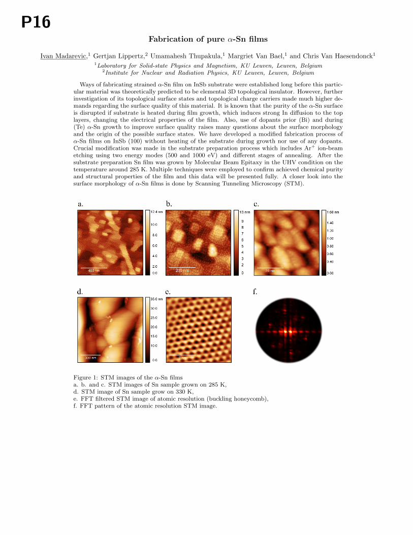
Figure 1 shows typical time-domain signals of p-polarized THz radiation from the samples. Fromall samples, clear transient signals of THz radiation were observed. It was found that the directionof the p-polarized THz field from Sb2Te3 is opposite to that from Bi2Te3. Based on the polarizationdependence of the emitted THz radiation, we attributed the generation process of p-polarized THzradiation mainly to transiently accelerated carriers parallel to the sample normal direction. Thedifference in the polarity of p-polarized THz fields observed for Sb2Te3 and Bi2Te3 implies that thephoto-induced instantaneous modification of the depletion field on the sample surfaces is the domi-nant mechanism of THz emission. [3] The shape of the p-polarized THz field for the Bi2Te3/Sb2Te3sample is different form others and hence is thought to be related to the interface state.
400 x10-6
200
0
-200Am
plitu
de (a
rb. u
nit)
121086420-2-4Time (ps)
Sb2Te3 Bi2Te3 Bi2Te3/Sb2Te3 (pn junction)
FIG. 1. Transient p-polarized THz emission signals for Sb2Te3, Bi2Te3, and Bi2Te3/Sb2Te3 films.
[1] K. Makino, S. Kuromiya, K. Takano, K. Kato, M. Nakajima, Y. Saito, J. Tominaga, H. Iida, M. Kinoshita, T. Nakano,ACS Appl. Mater. Interfaces 8, 32408 (2016).
[2] C.-M. Tu, T.-T. Yeh, W.-Y. Tzeng, Y.-R. Chen, H.-J. Chen, S.-A. Ku, C.-W. Luo, J.-Y. Lin, K.-H. Wu, J.-Y. Juang, T.Kobayashi, C.-M. Cheng, K.-D. Tsuei, H. Berger, R. Sankar and F.-C. Chou, Sci. Rep. 5, 14128 (2016).
[3] Z. Zhao, G. Niehues, S. Funkner, E. Estacio, Q. Han, K. Yamamoto, J. Zhang, W. Shi, Q. Guo,and M. Tani, Appl. Phys.Lett. 105, 231104 (2014).
P17
Spin polarization of Dirac-cone surface state at W(110) influenced by polarized light
Koji Miyamoto,1 Taichi Okuda,1 Henry Wortelen,2 Markus Donath,2 and Jurgen Henk3
1Hiroshima Synchrotron Radiation Center, Hiroshima University2Westfalische Wilhelms-Universitat Munster, Physikalisches Institut, Germany
3Martin-Luther-Universitat Halle-Wittenberg, Institut fur Physik, Germany
Recently, for the topological surface state (TSS) of Bi2Se3, several groups have observed aninteresting phenomenon by spin- and angle-resolved photoemission (SARPE): the observed spinfeatures of the photoelectrons are strongly dependent on the light polarization [1,2]. This effect iscurrently highly debated in the field of optospintronics. Although this effect might be dependent oncrystal symmetry, so far, the observations of the effect are limited to surfaces with C3v symmetry[1-3]. Very recently, we have discovered that the surface of W(110) shows a spin-polarized Dirac-conestate within a spin-orbit-induced gap, which is reminiscent of a TSS [4]. Here, in contrast to so-farstudied topological insulators, the surface structure has C2v symmetry. The C2v symmetry stronglyinfluences the dispersion of the Dirac-cone surface state, resulting in a flattened Dirac-cone. W(110)is suitable to research the spin feature of the photoelectrons dependent on the light polarization onmaterial with C2v.
We have studied the spin feature of Dirac-cone surface state along , at W(110), using SARPEspectroscopy with various light polarizations; left and right circular or s- and p- polarizations. Wehave noted that the observed spin feature of photoelectrons excited by p-polarized light is oppositeto the case of s-polarized light for tangential spin component. According to dipole selection rule,we can observe the spin feature of even orbital symmetry and odd orbital symmetry by p-polarizedlight and s-polarized light, respectively. In that, their results show the orbital dependence of spinfeature of the Dirac-cone-like surface state [5].
On the other hand, in the case of circular polarized light, not only tangential spin component butalso radial and out-of-plane spin component can be observed. The observed complex spin featureaccepts strongly influenced by C2v symmetry and is well reproduced by first-principles calculationincluding photoemission process. In detail, I introduce you in my presentation.
[1] C. Jozwiak et al., Nat., Phys. 9, 293 (2013).[2] Z. Xie et al., Nat., Commun. 5, 3382 (2013).[3] J. Sanchez-Barriga et al., Phys. Rev. X 4, 011046 (2014).[4] K. Miyamoto et al., Phys. Rev. Lett. 108, 066808 (2012).[5] K. Miyamoto et al., Phys. Rev. B 93, 161403 (2016).
P18
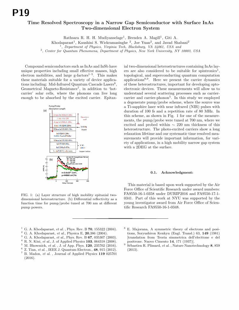
Time Resolved Spectroscopy in a Narrow Gap Semiconductor with Surface InAsTwo-dimensional Electron System
Rathsara R. H. H. Mudiyanselage1, Brenden A. Magill1, Giti A.
Khodaparast1, Kaushini S. Wickramasinghe 2, Joe Yuan2, and Javad Shabani21, Department of Physics, Virginia Tech, Blacksburg, VA 24061, USA and
2, Center for Quantum Phenomena, Department of Physics, New York University, NY 10003, USA
Compound semiconductors such as InAs and InSb haveunique properties including small effective masses, highelectron mobilities, and large g-factors1–5. This makesthese materials suitable for a variety of device applica-tions including: Mid-Infrared Quantum Cascade Lasers6,Geometrical Magneto-Resistance7, in addition to ‘hot-carrier’ solar cells, where the phonons can live longenough to be absorbed by the excited carrier. Epitax-
Doped
Supper Lattice
Pump/ProbeAbsorption Length
5
4
3
2
1
0
R
/R (%
)
6004002000Delay Time (ps)
JS 139, RT, Pump/Probe 700 nm 160 mW 100 mW 50 mW
Pump/Probe ratio 1/100
n=3.6x10¹¹ /cm2,μ=44860 cm2/Vs
(a)
(b)
FIG. 1: (a) Layer structure of high mobility epitaxial two-dimensional heterostructure. (b) Differential reflectivity as afunction time for pump/probe tuned at 700 nm at differentpump powers.
ial two-dimensional heterostructures containing InAs lay-ers are also considered to be suitable for spintronics1,topological, and superconducting quantum computationapplications8,9. Here we present the carrier dynamicsof these heterostructures, important for developing opto-electronic devices. These measurements will allow us tounderstand several scattering processes such as carrier-carrier and carrier-phonon5. In this study we employeda degenerate pump/probe scheme, where the source wasa Ti-sapphire laser with near infrared (NIR) pulses withduration of 100 fs and a repetition rate of 80 MHz. Inthis scheme, as shown in Fig. 1 for one of the measure-ments, the pump/probe were tuned at 700 nm, where weexcited and probed within ∼ 220 nm thickness of thisheterostructure. The photo-excited carriers show a longrelaxation lifetime and our systematic time resolved mea-surements will provide important information, for vari-ety of applications, in a high mobility narrow gap systemwith a 2DEG at the surface.
0.1. Acknowledgment:
This material is based upon work supported by the AirForce Office of Scientific Research under award numbers:FA9550-16-1-0358 under DURIP2016 and FA9550-17-1-0341. Part of this work at NYU was supported by theyoung investigator award from Air Force Office of Scien-tific Research FA9550-16-1-0348.
1 G. A. Khodaparast, et al. , Phys. Rev. B 70, 155322 (2004).2 G. A. Khodaparast, et al., Physica E, 20,386 (2004).3 G. A. Khodaparast, et al., Phys. Rev. B 67, 035307 (2003).4 R. N. Kini, et al., J. of Applied Physics 103, 064318 (2008).5 M. Bhowmick, et al. , J. of App. Phys. 120, 235702 (2016).6 Z. Tian, et al. , IEEE J. Quantum Electron., 48, 915 (2012).7 B. Madon, et al. , Journal of Applied Physics 119 025701
(2016).
8 E. Majorana, A symmetric theory of electrons and posi-tions, Soryushiron Kenkyu (Engl. Transl.) 63, 149 (1981)[translation from Teoria simmetrica dell’electtone e delpositrone. Nuovo Cimento 14, 171 (1937)].
9 Sebastien R. Plissard, et al. , Nature Nanotechnology 8, 859(2013).
P19
THz magneto photoresponse spectroscopy of structurally asymmetric
InAs/Al0.2Ga0.8Sb QW
Mehdi Pakmehr1,2, M. Gholami1, I. Lo2
1Shiraz University, Shiraz, 71946, Iran 2University at Buffalo (SUNY), Buffalo, 14260, USA
Corresponding author: [email protected]
InAs/GaSb semiconductor heterostructure were known as a prototype of broken gap type-II
quantum well (semimetalic) system for a while. Recently, it turns out that such
heterostructures could host novel quantum state of materials known as topological insulators
(2D case) due to its band inversion [1,2]. We studied band structure configuration of
InAs/Al0.2Ga0.8Sb heterostructure with broken gap (type II) band alignment through solving
8×8 Kane model Hamiltonian using vurgaftmans parameters. Due to Aluminum content of
QW (InAs) barrier layers we observe a smaller overlapping between conduction and valence
band at barrier regions. Furthermore, we investigated magneto-transport and THz magneto
photoresponse [3] properties of Hall bar samples made of MBE grown wafer with same
heterostructure configuration. The carrier density of QW region turns to be ns=7.6×1011 cm-2
obtained from quantum oscillation frequency (SdH ferq.) of Rxx signal at T=1.7 K. this
carrier density is such that sample has semimetalic phase with hall mobility of µ = 2.5×10⁵
cm-2/V·s. Results from two band model also confirms the broken band alignment of our
sample with phase transition at x=0.26 of alloying composition for barrier layers with 10 nm
thick InAs QW. The sample also exposed to chopped THz wave at f=2.53 THz to get PR
signal which have been used to extract different physical parameters of 2DEGs. Investigating
charge carrier properties of such novel heterostrcurure configurations could pave the way for
fabricating practical devices (e.g. transistors, IR lasers) benefiting properties of quantum
materials. We plan to present our findings for InAs/Al0.2Ga0.8Sb heterostructure system at
NGS18 conference.
References:
[1] C. Liu et al, PRL 100, 236601 (2008).
[2] I. Knez et al, PRL 107, 136603 (2011).
[3] M. Pakmehr et al, J. of Infrared, mm & THz waves 36, 291 (2015).
P20
Topological invariants for disordered systems
Pablo M. Perez-Piskunow,1 Dániel Varjas,2 Marcello D. Caio,3 Michel Fruchart,3 and Anton Akhmerov1
1Kavli Institute of Nanoscience, Delft University of Technology2QuTech, Delft University of Technolog
3Leiden University, Lorentz Institute
We present an algorithm to obtain real space markers of topological invariants, that do not rely on the periodicity ofthe system, and we use them to study disordered systems in various topological classes. In this algorithm, we boostthe efficiency of the topological markers by using the most localized approximation of the band projector.
The band projector is expanded with the kernel polynomial method (KPM) [1] and it is the most localizedapproximation, at a given energy resolution, for general hamiltonians. The efficiency of our algorithm relies on thelocality of the projector operator and its KPM expansion, where each moment of the expansion is obtained recursively,applying the Hamiltonian to a local vector. Each order of the expansion spreads the local vector in real space, and, atthe same time, increases the precission of the approximation in energy. Therefore, setting an energy resolution of theexpansion, also sets the minimum size of the sample, in order to mimic an infinite system.
We apply this systematic approach for the cases of 2D Chern makers [2] and 3D topological invariants in classes BDIand AIII [3, 4]. The algorithm can be further extended to other noncommutative expressions [5] for other topologicalclasses, making it a powerful tool to study the effect of disorder on the topology of large scale systems.
[1] A. Weisse, G. Wellein, A. Alvermann, H. Fehske, "The Kernel Polynomial Method". Rev. Mod. Phys. 78, 275-306 (2006).[2] R. Bianco and R. Resta, Mapping topological order in coordinate space. Phys. Rev. B 84, 241106(R) (2011).[3] I. Mondragon-Shem, T. L. Hughes, J. Song, and E. Prodan, "Topological Criticality in the Chiral-Symmetric AIII Class at
Strong Disorder". Phys. Rev. Lett. 113, 046802 (2014).[4] J. Song and E. Prodan, "AIII and BDI topological systems at strong disorder". Phys. Rev. B 89, 224203 (2014).[5] Hosho Katsura and Tohru Koma, "The Noncommutative Index Theorem and the Periodic Table for Disordered Topological
Insulators and Superconductors". arXiv:1611.01928v3 (2018).
P21
A Study of Bi-Te Stoichiometric Family:
Switching from Strong to Weak Topological Phase & Beyond
A. Jalil1,2, P. Schüffelgen1, M. Schleenvoigt1, M. Luysberg2, G. Mussler1, D. Grützmacher1
1 Peter Grünberg Institute -9, Forschungszentrum Jülich GmbH,
Wilhelm-Johnen-Straße 52425 Jülich, Germany 2 Ernst-Ruska Centre, Forschungszentrum Jülich GmbH,
Wilhelm-Johnen-Straße 52425 Jülich, Germany
Topological Insulator is relatively a new class of materials in condensed matter physics.
Strong spin-orbit coupling in such materials leads to band inversion which results in linearly
dispersed spin polarized energy states. Outcome of this phenomenon is appearance of metallic
(edge in case of 2D and surface in case of 3D) states with insulating bulk band structure being
protected by time reversal symmetry (TRS). 3D Topological Insulators are classified into two
categories i.e. strong topological insulators (STI), where all surfaces exhibit metallic behavior
and topology is protected by TRS; and weak topological insulators (WTI) where topology is
exhibited only by specific surfaces.
In this study we have focused on optimizing the growth of high quality thin film using
Molecular Beam Epitaxy (MBE), crystal structural analysis using X-Ray Diffraction (XRD)
and Scanning Transmission Electron Microscopy (STEM) and electronic structure
investigation using Angular-Resolved Photo Emission Spectroscopy (ARPES) of Bi-Te
stoichiometric compounds. Bi2Te3 is the most commonly known and heavily studied member
of this family. It contains the highest contents of Te and grows in the form of Quintuple
Layers (QL) with weak Van-der-Waals gaps. Bi2Te3 is a STI with all metallic surfaces
protected by TRS. Detailed structural analysis and electronic investigations are performed [1].
With controlled reduction of Te contents high quality thin films of Bi1Te1 are obtained [2].
Bi1Te1 is comprised of natural superlattice of alternating two Bi2Te3 QLs and one Bi bilayer.
It is found to exhibit the WTI behavior with non-protected trivial surfaces normal to the layer
stacking orientation. Along with WTI, it also exhibits partially polarized surface states away
from the Γ point which confirm the Topological Crystalline Insulator (TCI) phenomenon
where topology is not anymore protected by TRS rather by Crystal Symmetry (CS). Hence,
Bi1Te1 is a dual topological Insulator exhibiting WTI and TCI characteristics simultaneously
[2]. GW calculations are found to be in agreement with results obtained via ARPES. With
further controlled reduction of Te contents Bi4Te3 films have successfully been grown and are
subject to future investigations.
[1] J. Kampmeier, C. Weyrich, M. Lanius, M. Schall, E. Neumann, G. Mussler, T. Schäpers, D. Grützmacher:
Selective area growth of Bi2Te3 and Sb2Te3 topological insulator thin films, in: Journal of Crystal Growth
443 (2016) 38–42
[2] M. Eschbach, M. Lanius, C. Niu, E. Młyńczak, P. Gospodarič, J. Kellner, P. Schüffelgen, M. Gehlmann, S.
Döring, E. Neumann, M. Luysberg, G. Mussler, L. Plucinski, M. Morgenstern, D. Grützmacher, G.
Bihlmayer, S. Blügel, C. M. Schneider: Bi1Te1 is a dual topological insulator, in: Nat. Commun. 8, 14976
doi: 10.1038/ncomms14976 (2017)
P22
Towards Microscopic Control of the Magnetic ExchangeCoupling at the Surface of a Topological Insulator
Philipp Rußmann,1,∗ Phivos Mavropoulos,1,2 Gustav Bihlmayer,1 and StefanBlugel1
1Peter Grunberg Institut (PGI-1) and Institute for Advanced Simulation (IAS-1),Forschungszentrum Julich, D-52425 Julich, Germany
2Department of Physics, University of Athens, 15784 Zografou, Greece*Corresponding author: [email protected]
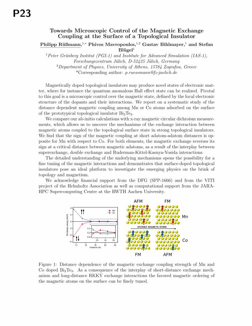
Magnetically doped topological insulators may produce novel states of electronic mat-ter, where for instance the quantum anomalous Hall effect state can be realized. Pivotalto this goal is a microscopic control over the magnetic state, defined by the local electronicstructure of the dopants and their interactions. We report on a systematic study of thedistance dependent magnetic coupling among Mn or Co atoms adsorbed on the surfaceof the prototypical topological insulator Bi2Te3.
We compare our ab-initio calculations with x-ray magnetic circular dichroism measure-ments, which allows us to uncover the mechanisms of the exchange interaction betweenmagnetic atoms coupled to the topological surface state in strong topological insulators.We find that the sign of the magnetic coupling at short adatom-adatom distances is op-posite for Mn with respect to Co. For both elements, the magnetic exchange reverses itssign at a critical distance between magnetic adatoms, as a result of the interplay betweensuperexchange, double exchange and Ruderman-Kittel-Kasuya-Yosida interactions.
The detailed understanding of the underlying mechanisms opens the possibility for afine tuning of the magnetic interactions and demonstrates that surface-doped topologicalinsulators pose an ideal platform to investigate the emerging physics on the brink oftopology and magnetism.
We acknowledge financial support from the DFG (SPP-1666) and from the VITIproject of the Helmholtz Association as well as computational support from the JARA-HPC Supercomputing Centre at the RWTH Aachen University.
Mn
Co
AFMFM
AFM FM
Figure 1: Distance dependence of the magnetic exchange coupling strength of Mn andCo doped Bi2Te3. As a consequence of the interplay of short-distance exchange mech-anism and long-distance RKKY exchange interactions the favored magnetic ordering ofthe magnetic atoms on the surface can be finely tuned.
P23
Surface effects in topological insulators A3Bi (A alkali element)
I.P. Rusinov,1, 2 P. Golub,3 I.Yu. Sklyadneva,1, 4, 5, 6 A. Isaeva,7 and E.V. Chulkov1, 2, 5
1Tomsk State University, pr. Lenina, 36, Tomsk, 634050 Russia2St. Petersburg State University, Universitetskaya nab., 7/9, St. Petersburg, 199034 Russia
3National University of Singapore, 117575 Singapore4Karlsruher Institut fur Technologie, Institut fur Festkorperphysik, D-76021 Karlsruhe, Germany
5Donostia International Physics Center (DIPC), Paseo de Manuel Lardizabal,4, 20018 San Sebastian/Donostia, Basque Country, Spain
6Institute of Strength Physics and Materials Science,pr. Academicheskii 2/1,634021, Tomsk, Russian Federation
7Technische Universitat Dresden, Bergstraße, 66, Dresden, D-01069, Germany
Surface electronic spectra, surface and bulk properties as well as the underlying chemical bondingcharacteristics are considered on the example of polar intermetallics KNa2Bi, K3Bi and Rb3Bi [1, 2].Chemical bonding in this materials have been analized within the Bader charge population analysis,and the MLWF technique. We pinpoint the emergent surface features in the electronic spectra thatare driven by the chemical bonding. Our findings build up a fundament for a more generalized,realistic study of polar intermetallics A3Bi within a model method and, hence, promote betterunderstanding of other topologically distinct systems with similar chemical bonding characteristics.
[1] I.Yu. Sklyadneva et al., Sci. Rep 6, 24137 (2016).[2] I.P. Rusinov et al., Phys. Rev. B 95, 224305 (2017).
P24
The Anomalous Hall Effect in Magnetic Topological Insulators
Amir Sabzalipour and Bart Partoens
Department of Physics, University of Antwerp, Belgium
We have studied the anomalous Hall effect (AHE) on the surface of a 3D magnetic topological
insulator, which provides a deep insight into the interplay between magnetism and the transverse
transport of massive Dirac Fermions due to an external applied electric field. In this work, the
AHE in a 3D TI is investigated using the semi-classical Boltzmann approach along with a modified
relaxation time scheme, in terms of the chemical potential of the system, the spatial orientation of
the surface magnetization and the concentration of magnetic and non-magnetic impurities. All
three different contributions to the AHE -the intrinsic berry-phase curvature effect, the extrinsic
side-jump and the skew scattering effects- are systematically treated. By applying a fully analytical
method we show how the relative importance of these contributions can be tuned, and can even
turn-off the AHE. For example it is shown that the anomalous Hall conductivity can even change
sign by altering the orientation of the surface magnetization, the concentration of the impurities
and also the position of the chemical potential, in agreement with recent experimental
observations.
P25
Sputter-grown 2D-TI/3D-TI stacking films in the Bi-Te binary system
Yuta Saito,1 Paul Fons,1 Kotaro Makino,1 Kirill V. Mitrofanov,1 Fumihiko
Uesugi,2 Masaki Takeguchi,2 Alexander V. Kolobov,1 and Junji Tominaga1
1Nanoelectronics Research Institute, National Institute of Advanced Industrial Science and Technology (AIST)2Transmission Electron Microscopy Station, National Institute for Materials Science (NIMS)
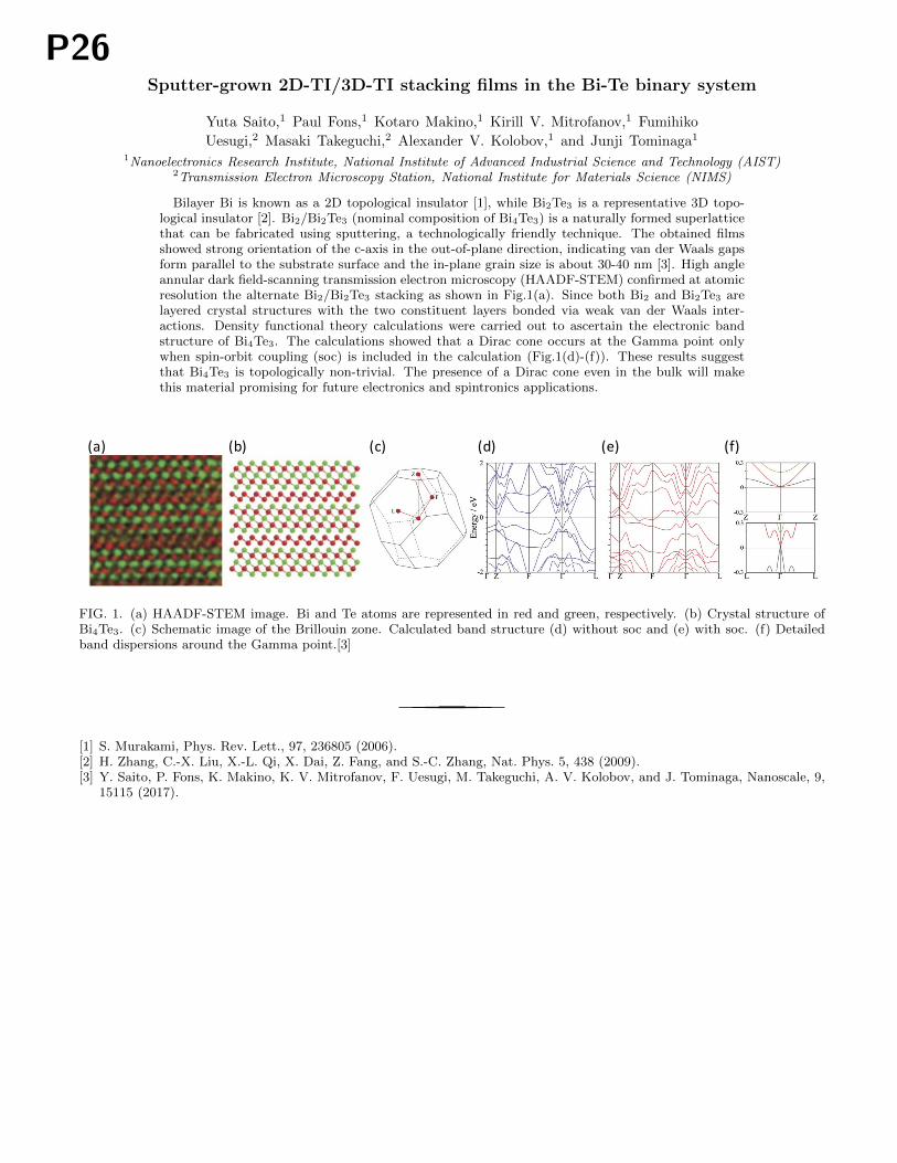
Bilayer Bi is known as a 2D topological insulator [1], while Bi2Te3 is a representative 3D topo-logical insulator [2]. Bi2/Bi2Te3 (nominal composition of Bi4Te3) is a naturally formed superlatticethat can be fabricated using sputtering, a technologically friendly technique. The obtained filmsshowed strong orientation of the c-axis in the out-of-plane direction, indicating van der Waals gapsform parallel to the substrate surface and the in-plane grain size is about 30-40 nm [3]. High angleannular dark field-scanning transmission electron microscopy (HAADF-STEM) confirmed at atomicresolution the alternate Bi2/Bi2Te3 stacking as shown in Fig.1(a). Since both Bi2 and Bi2Te3 arelayered crystal structures with the two constituent layers bonded via weak van der Waals inter-actions. Density functional theory calculations were carried out to ascertain the electronic bandstructure of Bi4Te3. The calculations showed that a Dirac cone occurs at the Gamma point onlywhen spin-orbit coupling (soc) is included in the calculation (Fig.1(d)-(f)). These results suggestthat Bi4Te3 is topologically non-trivial. The presence of a Dirac cone even in the bulk will makethis material promising for future electronics and spintronics applications.
(a) (b) (c) (d) (e) (f)
FIG. 1. (a) HAADF-STEM image. Bi and Te atoms are represented in red and green, respectively. (b) Crystal structure ofBi4Te3. (c) Schematic image of the Brillouin zone. Calculated band structure (d) without soc and (e) with soc. (f) Detailedband dispersions around the Gamma point.[3]
[1] S. Murakami, Phys. Rev. Lett., 97, 236805 (2006).[2] H. Zhang, C.-X. Liu, X.-L. Qi, X. Dai, Z. Fang, and S.-C. Zhang, Nat. Phys. 5, 438 (2009).[3] Y. Saito, P. Fons, K. Makino, K. V. Mitrofanov, F. Uesugi, M. Takeguchi, A. V. Kolobov, and J. Tominaga, Nanoscale, 9,
15115 (2017).
P26
Topological transport in noncollinear antiperovskites
Ilias Samathrakis,1 Harish Kumar Singh,1 and Hongbin Zhang1
1Institute of Materials Science, Otto-Berndt-Str. 3, 64287, Darmstadt, Germany
Antiferromagnetic (AFM) spintronics has recently become a hot research topic. In comparisonto ferromagnets, AFM materials are robust against perturbations due to magnetic fields and enablefaster switching frequency in the THz range. Non-collinear magnetic compounds, as one importantclass of AFM materials, have also attracted intensive attention and more specifically, Mn3Xsystems with X = Sn,Ge,Ga,Ir, and Rh have been proposed to host large intrinsic anomalous Hallconductivities [1],[2]. In this work, we performed first-principles calculations on the non-collinearantiperovskite Mn3GaN to investigate the behavior of the anomalous Hall conductivity (AHC)with respect to the magnetization direction. Our results reveal that the AHC displays a significantdependence with respect to the in-plane magnetization direction between the Γ5g and Γ4g magneticconfigurations where large anomalous Nernst effect can be induced by tailoring the magnetizationdirection. Moreover, we observed strong piezospintronic effect in Mn3GaN, where large AHC can beinduced by moderate epitaxial strain. Symmetry analysis reveals that for both cases, the nonzeroanomalous Hall conductivity is originated from the spin-orbit coupling instead of the noncollinearmagnetic configurations. Finally, we performed systematic high throughput screening for magneticcubic antiperovskites, and studied the magnetic ground state and the piezospintronic effect forthose compounds with noncollinear magnetic structure.
Acknowledgment: This work was supported by the Priority Program 1666 of the GermanResearch Foundation (DFG).
References
[1] A. K. Nayak et al., Science Advances, 2.4 (2016).[2] S. Nakatsuji, N. Kiyohara, and T. Higo, Nature 527.7577 (2015): 212
P27
Impact of Ultrafast Transport on the High-Energy States of a Photoexcited Topological Insulator
F. Freyse1, M. Battiato2, A. Varykhalov1, J. Sánchez-Barriga
1 1 Helmholtz-Zentrum Berlin für Materialien und Energie 2 12489 Berlin, Germany.
2 School of Physical and Mathematical Sciences, Nanyang Technological University, Singapore
Ultrafast dynamics in three-dimensional topological insulators (TIs) opens new routes for increasing the speed of information transport up to frequencies thousand times faster than in modern electronics. However, up to date, disentangling the exact contributions from bulk and surface transport to the subpicosecond dynamics of these materials remains a difficult challenge. Here, using time and angle-resolved photoemission, we demonstrate that driving a TI from the bulk-conducting into the bulk-insulating transport regime allows to selectively switch on and off the emergent channels of ultrafast transport between the surface and the bulk. We thus establish that ultrafast transport is one of the main driving mechanisms responsible for the decay of excited electrons in prototypical TIs following laser excitation. We further show how ultrafast transport strongly a?ects the thermalization and scattering dynamics of the excited states up to high energies above the Fermi level. In particular, we observe how inhibiting the transport channels leads to a thermalization bottleneck that substantially slows down electron-hole recombination via electron-electron scatterings. Our results pave the way for exploiting ultrafast transport to control thermalization time scales in TI-based optoelectronic applications, and expand the capabilities of TIs as intrinsic solar cells.
P28
Multistage chemical eath depossitiosn osf thic flm cadmium sulfde fosr ddS/ddee X-ra detectosr
H. Shamsa, H. Aeosu-Gaeala, M. Soslimane, S. Eerahime, S. Agam a a-Nuclear and Radiatiosn
Engineering Department, Facult osf Engineering, Alexandria Universit , Eg pt. e-Materials
Science Department, Institute osf Graduate Studies and Research, Alexandria Universit , Eg pt.
Aestract
Man methosds are used tos measure X-ra fux generated e mosdern X-ra machines. ehe
mosst cosmmosn methosd utiliied fosr mosnitosring X-ra dosse is technicall cosmplex and expensive.
In this wosr multila er osf cadmium sulfde ddS) using chemical eath depossitiosn dCD) were
carried osut tos depossit thic la er osptimum thic ness tos prosduce ddS/ddee junctiosn x-ra
detectosr. ehe efects osf the depossitiosn time, cadmium chlosride heat treatment, the ammosnia
and thiosurea cosncentratiosn osn ddS la ers were cosntroslled and investigated throsugh scanning
electrosn microsscospe SEM), energ dispersive x-ra anal sis EDXA), X-ra difractiosn XRD),
and ultravioslet UV)-visiele spectrosscosp . ehe XRD anal sis shoswed that the ddS flms have
highl osriented cr stallites with the classical hexagosnal structure wurtiite t pe) and the main
six difractiosn pea s. ehe relativel strosnger and narrosw pea osf ddS flm osetained with 6
stages alosng 002) plane indicated that the flm is highl osriented alosng the c-axis. ehe eand
gap Eg can ee extraposlated tos ee 2.41 eV. It was oseserved that the maximum and the
minimum amplitudes osf the pulse fosrmed due tos expossed FeO/ddS/ddee/Mos detectosr tos Xra
osf 33 eV and 1mA intensit are 0.732 and -0.405 V and cosnsequentl the tostal osutput
amplitude is 1.137 V. Ke wosrds: ddee; ddS; ehin flm; X-ra ; Detectosr
P29
Effect of Deformation on the Electronic Structure and Topological Properties of theAIIMg2Bi2 (AII = Mg,Ca,Sr,Ba) Compounds
I. V. Silkin,1 E. K. Petrov,1, 2 Yu. M. Koroteev,1, 3 and E. V. Chulkov1, 2, 4
1Tomsk State University, pr. Lenina, 36, 634050 Tomsk, Russia2St. Petersburg State University, Universitetskaya nab., 7/9, 199034 St. Petersburg, Russia
3Institute of Strength Physics and Materials Science, pr. Academicheskii 2/1, 634021, Tomsk4Donostia International Physics Center (DIPC), Paseo de Manuel Lardizabal,
4, 20018 San Sebastian/Donostia, Basque Country, Spain
Recently, much attention has been paid to the study of the properties of topological insulatorsand Dirac semimetals, which are of interest primarily due to their electronic structure featuresnear the Fermi level. The band structure of the surface of a topological insulator includes a Diraccone formed by two spin-polarized bands with linear dispersion intersecting at the Dirac point atthe Fermi level. In this case, the fundamental energy gap of the bulk material is inverted nearcertain high-symmetry points of the reciprocal space (so-called TRIM points). A Dirac semimetalis characterized by the presence of the Dirac cone formed by doubly degenerate bands in the bandstructure of the bulk crystal. Due to their exotic properties, these materials are promising in termsof their use in electronic devices of a new generation. Consequently, the search for compounds withsuch properties is an actual task for creation of the elemental base of new electronics.
We present the results of an initial theoretical study of the electronic structure and topologicalproperties of the AIIMg2Bi2 (AII = Mg, Ca, Sr, Ba) compounds in the equilibrium state, under thehydrostatic pressure and uniaxial deformation.
It has been shown that the Mg3Bi2 compound in the equilibrium state is a semimetal, whereasthe CaMg2Bi2, SrMg2Bi2 and BaMg2Bi2 compounds are semiconductors with a direct fundamentalband gap. In the case of hydrostatic pressure in the three-component compounds, we have revealed asemiconductor–semimetal transition without change in the topological properties. Uniaxial tensionof the CaMg2Bi2, SrMg2Bi2 and BaMg2Bi2 compounds results in the transition from the semicon-ductor to the Dirac semimetal phase. Uniaxial compression leads to a richer spectrum of the observedelectron phases. In the CaMg2Bi2 compound, the semiconductor–topological insulator–topologicalsemimetal sequence is realized, in the SrMg2Bi2 compound the semiconductor–Dirac semimetal–topological insulator–topological semimetal, and the BaMg2Bi2 semiconductor–topological insula-tor. Therefore, it becomes possible to control topological properties of the CaMg2Bi2, SrMg2Bi2 andBaMg2Bi2 compounds by uniaxial tension or compression. In the case of the Mg3Bi2 compound,none of the deformations considered leads to qualitative changes in the band structure and topo-logical properties. Owing to the rich spectrum of topologically nontrivial phases, the compoundsCaMg2Bi2, SrMg2Bi2 and BaMg2Bi2 may be of interest for further theoretical and experimentalstudies [1].
[1] E. K. Petrov, I. V. Silkin, Yu. M. Koroteev, E. V. Chulkov, JETP Lett. 105, 491 (2017)
P30
P31
Optical and elastic properties of the topological insulator Bi1.5Sb0.5Te1.8Se1.2: Role ofbulk defects
I.V. Zhevstovskikh,1, 2 Yu.S. Ponosov,1,2 S.G. Titova,2, 3 N.S. Averkiev,4 V.V.
Gudkov,2 M. N. Sarychev,2 T.V. Kuznetsova,1, 2 K.A. Kokh,5 and O.E. Tereshchenko6
1M.N. Miheev Institute of Metal Physics UB RAS, Ekaterinburg 620137, Russia2Ural Federal University, Ekaterinburg 620002, Russia
3Institute of Metallurgy, UB RAS, Ekaterinburg 620016, Russia4Ioffe Institute, St. Petersburg 194021, Russia
5V.S. Sobolev Institute of Geology and Mineralogy, SB RAS, Novosibirsk 630090, Russia6A.V. Rzanov Institute of Semiconductor Physics, SB RAS, Novosibirsk 630090, Russia
Recently, the quaternary Bi2−xSbxTe3−ySey compound has exhibited pronounced topological sur-face states with an insulating bulk [1–4]. It was found that, at (x,y)=(0.5,1.3) (Bi1.5Sb0.5Te1.7Se1.3),the electron and hole carriers compensation is maximally realized. The bulk-insulating behavior inthe Bi2−xSbxTe3−ySey solid solution is achieved by introducing two prevailing types of chargeddefects, such as (Bi,Sb)/Te antisite defects and the Se vacancy defects [1]. However, other defectscan also be formed. To characterize the bulk defects in the topological insulators non-destructivelocal probes, which should be performed on the same sample, are needed, because the presence ofpoint defects in the sample depends on the growth conditions and their random distribution acrossthe crystal is difficult to control. In this report, we present the experimental studies of the optical,elastic and structural properties of the Bi1.5Sb0.5Te1.8Se1.2 single crystal and compare them to thoseto binary tetradymite Bi2Te3.
High-quality Bi1.5Sb0.5Te1.8Se1.2 and Bi2Te3 single crystals were grown by the modified Bridg-man technique with a temperature gradient of about 10 K·cm−1 at the front of crystallization [5].The crystal structure of Bi1.5Sb0.5Te1.8Se1.2 and Bi2Te3 samples was determined using the X-raypowder diffraction with diffractometer Shimadzu XRD 7000 Maxima (Cu Kα-radiation, graphitemonochromator, scattering angle range 2ϑ = 15◦ − 71.5◦ at room temperature, and 20◦ − 70◦ atlower and higher temperatures). The samples patterns are essentially the same and can be wellindexed with the rhombohedral structure, confirming that the Bi1.5Sb0.5Te1.8Se1.2 maintains thesame crystal structure as Bi2Te3.
We found the anomalous behavior of the elastic and optical properties in Bi1.5Sb0.5Te1.8Se1.2
that is absent in Bi2Te3. The extra vibrational excitation was observed in the Raman spectrumnear 125 cm−1. Its line width has increased substantially with the increasing temperature, and itsfrequency showed a sharp softening in the temperature range of 200-250 K. In the same temperaturerange, a large peak in attenuation of longitudinal ultrasound wave propagating along the trigonalaxis and the step-like anomaly on the temperature-dependence of elastic modulus C33 were found.We revealed a correlation between the anomalous behavior of the elastic and optical properties andsuggested that they are of a common nature and caused by bulk defects with a low symmetry. Thesedefects are most likely located in the upper Te/Se and Bi/Sb quintuple layers, the most suitableones are pairs: Se interstitial+(Bi,Sb)/Te antisite defects. The activation energy of the defect of 78meV determined from the temperature dependence of the relaxation time is likely to represent thethermal barrier for hopping processes. The importance of our results is in the identification of anew type of defects in Bi1.5Sb0.5Te1.8Se1.2, which can affect the transport, thermoelectric and otherproperties not only in the bulk, but also on the surface of three-dimensional topological insulators.
[1] Zhi Ren, A.A. Taskin, Satoshi Sasaki, Kouji Segava, and Yoichi Ando. Phys. Rev. B 84, 165311 (2011).[2] A.A. Taskin, Zhi Ren, Satoshi Sasaki, Kouji Segava, and Yoichi Ando. Phys. Rev. Lett. 107, 016801 (2011).[3] T. Arakane, T. Sato, S. Souma, K. Kosaka, K. Nakayama, M. Komatsu, T. Takahashi, Zhi Ren, Kouji Segava,
and Yoichi Ando. Nature Comm. 3, 363 (2012).[4] M.V. Filianina, I.I. Klimovskikh, I.A.Shvets, A.G. Rybkin, A.E. Petukhov, E.V.Chulkov, V.A. Golyashov,
K.A. Kokh, O.E. Tereshchenko, C. Polley, T. Balasubramanian, M. Leandersson, A.M. Shikin. MaterialsChem. and Phys. 207, 253 (2018).
[5] K. A. Kokh , S. V. Makarenko , V. A. Golyashov , O. A. Shegai , O. E. Tereshchenko , Cryst. Eng. Comm.16, 581 (2014).
P32
Topological quantum phase transition from mirror to time reversal symmetry protected topological insulator
Partha S. Mandal1, Gunther Springholz2, Valentine V. Volobuev2,3, Ondrej Caha4, Andrei Varykhalov1, Evangelos Golias1, Günther Bauer2, Oliver Rader1, Jaime Sánchez-Barriga1
1 1 Helmholtz-Zentrum Berlin für Materialien und Energie, Albert-Einstein Strasse 15,
2 12489 Berlin, Germany. 2 Institute for Semiconductor and Solid State Physics, Johannes Kepler Universität,
Altenberger Strasse 69, 4040 Linz, Austria. 3 National Technical University “Kharkiv Polytechnic Institute”, Frunze Street 21, 61002 Kharkiv,
Ukraine. 3 4 Department of Condensed Matter Physics, Masaryk University, Kotlářská 267/2,
4 61137 Brno, Czech Republic
Topological insulators constitute a new phase of matter protected by symmetries. Time-reversal symmetry protects strong topological insulators of the Z2 class, which possess an odd number of metallic surface states with dispersion of a Dirac cone. Topological crystalline insulators are less robust and merely protected by individual crystal symmetries. They show an even number of Dirac cones. In this work, it is demonstrated that Bi doping of Pb1−xSnxSe (111) epilayers induces a quantum phase transition from a topological crystalline insulator to a Z2 topological insulator. This occurs because Bi-doping lifts the fourfold valley degeneracy and induces a gap at Γ, while the three Dirac cones at the M points of the surface Brillouin zone remain intact. We interpret this new phase transition as caused by a lattice distortion. It implies that the system becomes ferroelectric. Our results demonstrate that strong topological insulators can be switchable by distortions or electric fields. [1] P. S. Mandal, G. Springholz, V. V. Volobuev, O. Caha, A. Varykhalov, E. Golias, G. Bauer, O. Rader, J. Sánchez-Barriga, Nat. Commun. 8, 968 (2017)
P33


![Apeiron Volume 39 Issue 3 2006 [Doi 10.1515%2FAPEIRON.2006.39.3.257] Henry, Devin -- Understanding Aristotle's Reproductive Hylomorphism](https://static.fdocument.org/doc/165x107/55cf9002550346703ba25178/apeiron-volume-39-issue-3-2006-doi-1015152fapeiron2006393257-henry.jpg)


![37ο ΕΤΗΣΙΟ ΣΥΝΕΔΡΙΟ · 2015-05-24 · Συνεδρία 10η Αίθουσα Β’ Παρουσίαση και συζήτηση posters P8 [57-64] 12.30 – 13.30 Συνεδρία](https://static.fdocument.org/doc/165x107/5f10b1ac7e708231d44a5d2c/37-2015-05-24-10-f.jpg)
