
Photolithographic solutions for image sensors with high pixel … Workshops/2013 Worksho… · ·...
4
Table.1: Major specifications of FPA-5510iZ Specification Magnification 4:1 NA 0.45~0.57 Field Size 26 x 33mm Resolution ≤0.35mm Wavelength 365nm σ Aperture 0.40~0.75 (@NA0.57) Intensity ≥34,500W/m2 (@ NA0.57 / σ0.70) ≤ 18nm 8~21% Item Projection Lens Illumination Overlay Accuracy Oxygen Concentration Photolithographic solutions for image sensors with high pixel density Ryo Sasaki, Yuhei Sumiyoshi, Yasuo Hasegawa and Seiya Miura Canon Inc. 20-2, Kiyohara-Kogyodanchi, Utsunomiya-shi, Tochigi 321-3292, Japan TEL: +81-28-667-5711, FAX: +81-28-667-8799, Email: [email protected] Abstract An increasing number of technical challenges have arisen in the image sensor manufacturing process, such as wafer distortion in backside illumination (BSI) processes and reticle distortion in colour filter (CF) processes. In this paper, Canon lithographic solutions that optimise both alignment and exposure performance are explained in detail. Exposure results with these solutions applied are also presented. Introduction The increase in the number of pixels in image sensors has been accelerating pixel shrink. To establish a manufacturing process for smaller pixels, overlay accuracy improvement of photolithography equipment is the key technical challenge, because each pixel must be precisely overlaid to various layers, colour filters and micro-lenses. BSI image sensors, the current mainstream of CMOS sensors, enhance light sensitivity by applying a structure that receives light from the backside of circuit patterns, eliminating the vignetting of light from the circuit. In the manufacturing process, the back side of a patterned wafer is ground to a thickness of a few microns (μm) after being bonded to a supported wafer. This bonding and thinning process causes large distortion to the wafer, resulting in the deformation of shot shape that are pre-exposed by exposure equipment during the circuit pattern process. In the next process, the colour filter process, CF patterns need to be exposed on the distorted shots with high accuracy, which is one of the main technical challenges for high productivity. Semiconductor exposure equipment generally adopt a global alignment system, which measures four or eight sample shots on a wafer and linearly calculates overlay information such as shift, rotation and magnification of shots. However, non-linear errors caused by wafer distortion in BSI processes have become an enormous technical challenge in mass production. Moreover, it is necessary to detect alignment marks from the back side of Si wafers since alignment marks are located on the circuit pattern side. In addition, high exposure dose required in CF processes must be carefully considered to improve overlay accuracy. Negative resists, generally used in CF processes, are widely known for inhibition of polymerization due to oxygen in the air. This effect requires larger exposure dose in CF processes, resulting in the deterioration of overlay accuracy. Lithographic solutions to technical challenges in manufacturing process of image sensors 1) Introduction of the FPA-5510iZ The FPA-5510iZ has been developed as an exposure system to solve the above mentioned issues. A list of major specifications of the FPA-5510iZ is shown in Table 1. The FPA-5510iZ, equipped with functions on the table, is an ideal exposure system for BSI and CF exposure processes.
Transcript of Photolithographic solutions for image sensors with high pixel … Workshops/2013 Worksho… · ·...
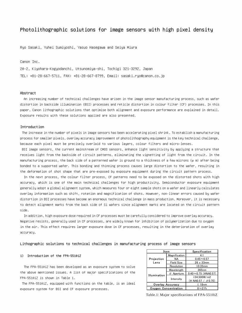
Table.1: Major specifications of FPA-5510iZ
Specif ication
Magnification 4:1NA 0.45~0.57
Field Size 26 x 33mmResolution ≤0.35mm
Wavelength 365nmσ Aperture 0.40~0.75 (@NA0.57)
Intensity≥34,500W/m2
(@ NA0.57 / σ0.70)
≤ 18nm
8~21%
Item
ProjectionLens
I llumination
Overlay Accuracy
Oxygen Concentration
Photolithographic solutions for image sensors with high pixel density
Ryo Sasaki, Yuhei Sumiyoshi, Yasuo Hasegawa and Seiya Miura
Canon Inc.
20-2, Kiyohara-Kogyodanchi, Utsunomiya-shi, Tochigi 321-3292, Japan
TEL: +81-28-667-5711, FAX: +81-28-667-8799, Email: [email protected]
Abstract
An increasing number of technical challenges have arisen in the image sensor manufacturing process, such as wafer
distortion in backside illumination (BSI) processes and reticle distortion in colour filter (CF) processes. In this
paper, Canon lithographic solutions that optimise both alignment and exposure performance are explained in detail.
Exposure results with these solutions applied are also presented.
Introduction
The increase in the number of pixels in image sensors has been accelerating pixel shrink. To establish a manufacturing
process for smaller pixels, overlay accuracy improvement of photolithography equipment is the key technical challenge,
because each pixel must be precisely overlaid to various layers, colour filters and micro-lenses.
BSI image sensors, the current mainstream of CMOS sensors, enhance light sensitivity by applying a structure that
receives light from the backside of circuit patterns, eliminating the vignetting of light from the circuit. In the
manufacturing process, the back side of a patterned wafer is ground to a thickness of a few microns (μm) after being
bonded to a supported wafer. This bonding and thinning process causes large distortion to the wafer, resulting in
the deformation of shot shape that are pre-exposed by exposure equipment during the circuit pattern process.
In the next process, the colour filter process, CF patterns need to be exposed on the distorted shots with high
accuracy, which is one of the main technical challenges for high productivity. Semiconductor exposure equipment
generally adopt a global alignment system, which measures four or eight sample shots on a wafer and linearly calculates
overlay information such as shift, rotation and magnification of shots. However, non-linear errors caused by wafer
distortion in BSI processes have become an enormous technical challenge in mass production. Moreover, it is necessary
to detect alignment marks from the back side of Si wafers since alignment marks are located on the circuit pattern
side.
In addition, high exposure dose required in CF processes must be carefully considered to improve overlay accuracy.
Negative resists, generally used in CF processes, are widely known for inhibition of polymerization due to oxygen
in the air. This effect requires larger exposure dose in CF processes, resulting in the deterioration of overlay
accuracy.
Lithographic solutions to technical challenges in manufacturing process of image sensors
1) Introduction of the FPA-5510iZ
The FPA-5510iZ has been developed as an exposure system to solve
the above mentioned issues. A list of major specifications of the
FPA-5510iZ is shown in Table 1.
The FPA-5510iZ, equipped with functions on the table, is an ideal
exposure system for BSI and CF exposure processes.
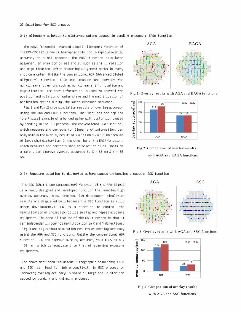
Fig.2: Comparison of overlay results
with AGA and EAGA functions
overlay accuracy[nm]
114
85
129
85
0
50
100
150
AGA EAGA
dx dy
Fig.4: Comparison of overlay results
with AGA and SSC functions
overlay accuracy[nm]
114
25
129
32
0
50
100
150
AGA SSC
dx dy
AGA EAGA
Fig.1: Overlay results with AGA and EAGA functions
AGA SSC
Fig.3: Overlay results with AGA and SSC functions
2) Solutions for BSI process
2-1) Alignment solution to distorted wafers caused in bonding process: EAGA function
The EAGA (Extended Advanced Global Alignment) function of
the FPA-5510iZ is one lithographic solution to improve overlay
accuracy in a BSI process. The EAGA function calculates
alignment information of all shots, such as shift, rotation
and magnification, after measuring alignment marks in every
shot on a wafer. Unlike the conventional AGA (Advanced Global
Alignment) function, EAGA can measure and correct for
non-linear shot errors such as non-linear shift, rotation and
magnification. The shot information is used to control the
position and rotation of wafer stage and the magnification of
projection optics during the wafer exposure sequence.
Fig.1 and Fig.2 show simulation results of overlay accuracy
using the AGA and EAGA functions. The functions are applied
to a typical example of a bonded wafer with distortion caused
by bonding in the BSI process. The conventional AGA function,
which measures and corrects for linear shot information, can
only obtain the overlay result of X = 114 nm & Y = 129 nm because
of large shot distortion. On the other hand, the EAGA function,
which measures and corrects shot information of all shots on
a wafer, can improve overlay accuracy to X = 85 nm & Y = 85
nm.
2-2) Exposure solution to distorted wafers caused in bonding process: SSC function
The SSC (Shot Shape Compensator) function of the FPA-5510iZ
is a newly designed and developed function that enables high
overlay accuracy in BSI process. (In this paper, simulation
results are displayed only because the SSC function is still
under development.) SSC is a function to control the
magnification of projection optics in step and repeat exposure
equipment. The special feature of the SSC function is that it
can independently control magnification in X and Y directions.
Fig.3 and Fig.4 show simulation results of overlay accuracy
using the AGA and SSC functions. Unlike the conventional AGA
function, SSC can improve overlay accuracy to X = 25 nm & Y
= 32 nm, which is equivalent to that of scanning exposure
equipments.
The above mentioned two unique lithographic solutions; EAGA
and SSC, can lead to high productivity in BSI process by
improving overlay accuracy in spite of large shot distortion
caused by bonding and thinning process.
2-
m
Ho
of
te
sy
S
co
ob
be
a
tr
of
77
th
sy
a
to
pr
3)
3-
D
to
te
fu
be
F
su
d
re
to
T
in
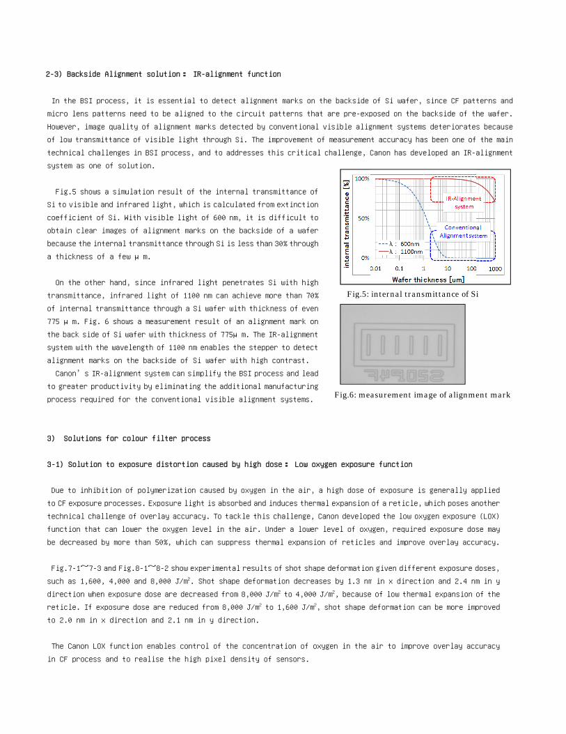
-3) Backside A
In the BSI pro
icro lens patt
owever, image
f low transmit
echnical chal
ystem as one o
Fig.5 shows a
i to visible an
oefficient of
btain clear im
ecause the int
thickness of
On the other
ransmittance,
f internal tra
75 μm. Fig. 6
he back side o
ystem with the
lignment mark
Canon’s IR-a
o greater prod
rocess require
) Solutions
-1) Solution
Due to inhibit
o CF exposure p
echnical chal
unction that c
e decreased by
Fig.7-1~7-3 a
uch as 1,600,
irection when
eticle. If exp
o 2.0 nm in x
The Canon LOX
n CF process a
Alignment sol
ocess, it is e
terns need to
quality of a
ttance of vis
lenges in BSI
of solution.
a simulation
nd infrared li
Si. With visi
mages of alig
ernal transmit
a few μm.
hand, since
infrared lig
ansmittance th
6 shows a meas
of Si wafer wit
e wavelength o
s on the back
alignment syst
ductivity by e
ed for the co
for colour fi
to exposure d
tion of polyme
processes. Exp
lenge of overl
can lower the
y more than 5
and Fig.8-1~8
4,000 and 8,
exposure dose
posure dose ar
direction an
function ena
and to realis
ution: IR-al
essential to
be aligned t
lignment mark
ible light thr
process, and
result of the
ght, which is
ible light of
gnment marks o
ttance through
infrared ligh
ht of 1100 nm
hrough a Si wa
surement resu
th thickness o
of 1100 nm ena
kside of Si wa
tem can simpli
eliminating th
onventional vi
lter process
distortion cau
erization cau
posure light i
lay accuracy.
oxygen level
0%, which can
8-2 show exper
000 J/m2. Shot
e are decrease
re reduced fro
nd 2.1 nm in y
ables control
se the high pi
lignment funct
detect alignm
o the circuit
s detected by
rough Si. The
to addresses
internal tra
calculated fr
600 nm, it is
on the backsid
h Si is less tha
ht penetrates
can achieve
afer with thic
lt of an alig
of 775μm. The
ables the step
afer with high
fy the BSI pro
he additional m
isible alignme
used by high
sed by oxygen
s absorbed and
To tackle thi
in the air.
n suppress the
imental result
t shape defor
ed from 8,000
om 8,000 J/m2
y direction.
of the concen
ixel density o
tion
ment marks on
t patterns tha
y conventional
improvement o
this critica
nsmittance of
rom extinction
s difficult to
de of a wafer
an 30% through
Si with high
more than 70%
ckness of even
nment mark on
e IR-alignment
pper to detect
h contrast.
ocess and lead
manufacturing
ent systems.
dose: Low ox
n in the air,
d induces therm
s challenge,
Under a lower
ermal expansio
ts of shot shap
mation decrea
J/m2 to 4,000
to 1,600 J/m2,
ntration of ox
of sensors.
Fig.5:
Fig.6: me
the backside
at are pre-exp
visible alig
of measuremen
l challenge, C
f
n
o
h
h
%
n
n
t
t
d
g
xygen exposur
a high dose o
mal expansion
Canon develop
r level of oxy
on of reticle
pe deformation
ases by 1.3 nm
J/m2, because
, shot shape d
xygen in the
internal trans
asurement im
of Si wafer,
posed on the b
gnment systems
t accuracy ha
Canon has deve
e function
of exposure is
of a reticle,
ped the low oxy
ygen, required
es and improve
n given differ
m in x directi
e of low therm
deformation ca
air to improv
smittance of Si
mage of alignme
since CF patt
backside of th
s deteriorates
s been one of
eloped an IR-a
s generally ap
which poses an
ygen exposure
d exposure dos
e overlay accu
ent exposure d
ion and 2.4 nm
al expansion o
an be more imp
ve overlay acc
i
ent mark
terns and
he wafer.
s because
the main
alignment
pplied
nother
(LOX)
se may
uracy.
doses,
m in y
of the
proved
curacy
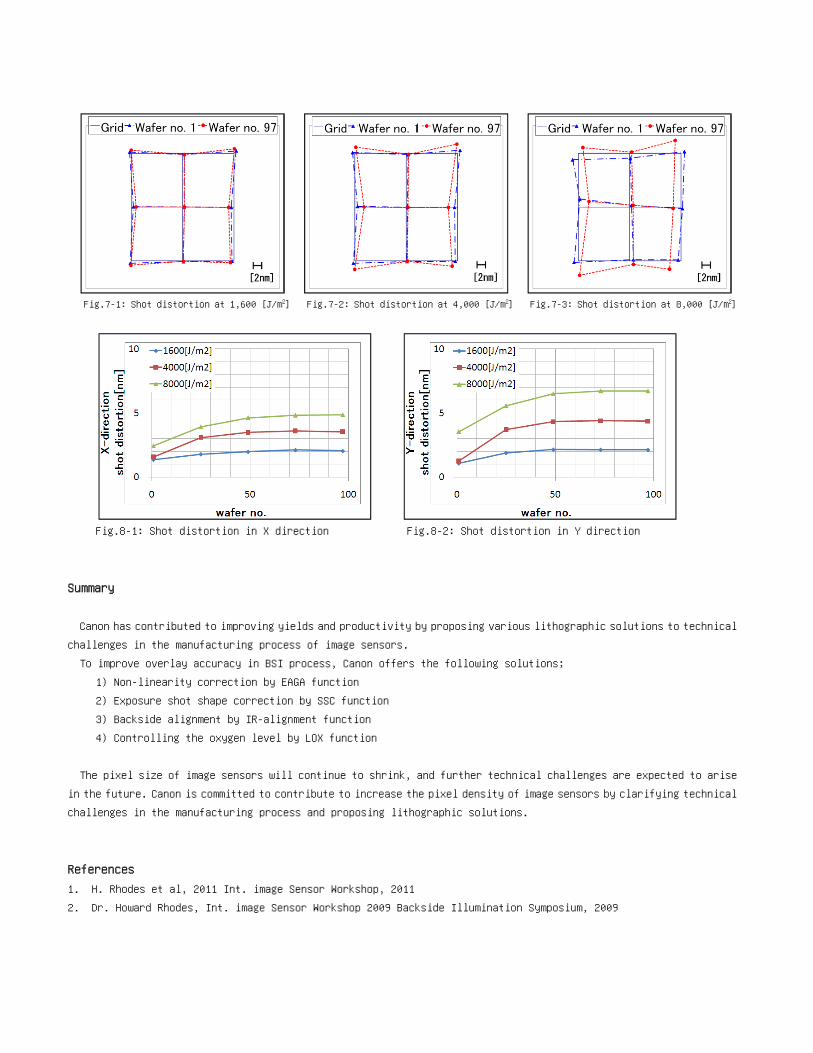
Fig.7-1: Shot distortion at 1,600 [J/m2] Fig.7-2: Shot distortion at 4,000 [J/m2] Fig.7-3: Shot distortion at 8,000 [J/m2]
Fig.8-1: Shot distortion in X direction Fig.8-2: Shot distortion in Y direction
Summary
Canon has contributed to improving yields and productivity by proposing various lithographic solutions to technical
challenges in the manufacturing process of image sensors.
To improve overlay accuracy in BSI process, Canon offers the following solutions;
1) Non-linearity correction by EAGA function
2) Exposure shot shape correction by SSC function
3) Backside alignment by IR-alignment function
4) Controlling the oxygen level by LOX function
The pixel size of image sensors will continue to shrink, and further technical challenges are expected to arise
in the future. Canon is committed to contribute to increase the pixel density of image sensors by clarifying technical
challenges in the manufacturing process and proposing lithographic solutions.
References
1. H. Rhodes et al, 2011 Int. image Sensor Workshop, 2011 2. Dr. Howard Rhodes, Int. image Sensor Workshop 2009 Backside Illumination Symposium, 2009