
Featuring super-high accuracy and multi-channel capabilities

Delft University of Technology
In-Pixel temperature sensors with an accuracy of ±0.25 °C, a 3σ variation of ±0.7 °C inthe spatial domain and a 3σ variation of ±1 °C in the temporal domain
Abarca, Accel; Theuwissen, Albert
DOI10.3390/mi11070665Publication date2020Document VersionFinal published versionPublished inMicromachines
Citation (APA)Abarca, A., & Theuwissen, A. (2020). In-Pixel temperature sensors with an accuracy of ±0.25 °C, a 3σvariation of ±0.7 °C in the spatial domain and a 3σ variation of ±1 °C in the temporal domain.Micromachines, 11(7), [665]. https://doi.org/10.3390/mi11070665
Important noteTo cite this publication, please use the final published version (if applicable).Please check the document version above.
CopyrightOther than for strictly personal use, it is not permitted to download, forward or distribute the text or part of it, without the consentof the author(s) and/or copyright holder(s), unless the work is under an open content license such as Creative Commons.
Takedown policyPlease contact us and provide details if you believe this document breaches copyrights.We will remove access to the work immediately and investigate your claim.
This work is downloaded from Delft University of Technology.For technical reasons the number of authors shown on this cover page is limited to a maximum of 10.
micromachines
Article
In-Pixel Temperature Sensors with an Accuracy of±0.25 C, a 3σ Variation of ±0.7 C in the SpatialDomain and a 3σ Variation of ±1 C in theTemporal Domain
Accel Abarca 1,* and Albert Theuwissen 1,2
1 Electronic Instrumentation Lab., Microelectronics, EWI, Delft University of Technology, 2628 CD Delft,The Netherlands; [email protected]
2 Harvest Imaging, 3960 Bree, Belgium* Correspondence: [email protected]
Received: 12 June 2020; Accepted: 6 July 2020; Published: 8 July 2020
Abstract: This article presents in-pixel (of a CMOS image sensor (CIS)) temperature sensors withimproved accuracy in the spatial and the temporal domain. The goal of the temperature sensors is tobe used to compensate for dark (current) fixed pattern noise (FPN) during the exposure of the CIS.The temperature sensors are based on substrate parasitic bipolar junction transistor (BJT) and on thenMOS source follower of the pixel. The accuracy of these temperature sensors has been improvedin the analog domain by using dynamic element matching (DEM), a temperature independent biascurrent based on a bandgap reference (BGR) with a temperature independent resistor, correlateddouble sampling (CDS), and a full BGR bias of the gain amplifier. The accuracy of the bipolarbased temperature sensor has been improved to a level of ±0.25 C, a 3σ variation of ±0.7 C inthe spatial domain, and a 3σ variation of ±1 C in the temporal domain. In the case of the nMOSbased temperature sensor, an accuracy of ±0.45 C, 3σ variation of ±0.95 C in the spatial domain,and ±1.4 C in the temporal domain have been acquired. The temperature range is between −40 Cand 100 C.
Keywords: in-pixel temperature sensors; Tixel; dark current; CMOS image sensor
1. Introduction
Nowadays, CMOS image sensors are widely used in different applications like astronomy,medicine, and especially in mobile phones [1–3]. For many years charge coupled devices (CCDs)dominated the field of image sensors in all kind of related applications. However, the appearance ofthe active pixel sensor (APS) emerged as a replacement of CCDs [4]. In the last decades, efforts toimprove the performance of APS have been made. Currently, the APS has several advantages overCCD like lower cost, lower power consumption, higher dynamic range, and higher integrability [5–7].At the same time, CMOS based temperature sensors are used in many applications like on-chip thermalcontrol, human body temperature monitoring, processor speed, and even in food monitoring [8–10].The dark current or leakage current of the CIS is one of the major contributors of FPN and becomesimportant under low light condition and high temperature variations. The dark current linearlydepends on the integration time of the pixels and exponentially on the temperature variation [11].In fact, the dark current doubles every ~5–10 C [12–14]. Different techniques are applied to compensatefor the dark current. The most common one is to take a dark reference frame at the beginning ofthe picture acquisition, at a certain exposure time with closed shutter, and then subtracting this darkreference frame from the following images. However, the temperature must be kept constant during
Micromachines 2020, 11, 665; doi:10.3390/mi11070665 www.mdpi.com/journal/micromachines
Micromachines 2020, 11, 665 2 of 16
the acquisition, otherwise the dark current level changes and a new dark reference frame should betaken. Also, modifications of the photodetector at the physical level have been made to reduce theeffect of the dark current. For instance, by adding a p-well layer surrounding the pixel [15], or by usinga buried-channel source follower instead of a surface-mode source follower [16].
In our previous works [17,18], the concept of integrating CMOS based temperature sensorshas been proved. Nevertheless, our temperature sensors need some improvement to reach a better3σ variation (spatial and temporal) to compensate for dark current more accurately. In this article,improvements of the in-pixel temperature sensors by using DEM, CDS, BGR bias current and BGRvoltage references, and sequential compensation to increase the accuracy of the temperature sensors ina wider temperature range are presented.
This article is organized as follows. Section 2 briefly explains the architecture of the sensorincluding the temperature sensors. In Section 3, sources of inaccuracy in temperature sensors arediscussed. The circuits to overcome the sources of inaccuracy are presented in Section 4. In Section 5,measurement results are presented. A conclusion is given at the end of this paper.
2. CMOS Image Sensor with In-Pixel Temperature Sensors
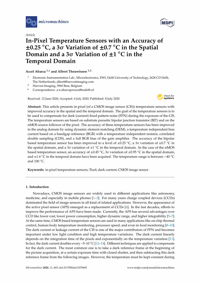
The block diagram of the CIS is shown in Figure 1. The sensor is composed of row and columndecoders, the pixel array of 60 × 140 pixels, and the readout circuit. Temperature measurements canbe performed either by the substrate parasitic bipolar or by the pixel itself via the source follower(SF) transistor. In the pixel array, 20 pixels have been replaced by bipolar temperature sensor pixels(Tixels), and they can perform temperature measurements at the same time as the pixels at the cost ofone dead pixel at the position of each Tixel. In the case of the SF temperature sensor, it is the pixelitself performing temperature and video measurements but in different phases incurring in a framelost. Pixels and temperature sensors use the same readout system composed of a programmable gainamplifier (PGA), a sample and hold (S/H) circuit, an output buffer, and an off-chip 16 bits ADC.
Micromachines 2020, 11, x FOR PEER REVIEW 2 of 16
reference frame should be taken. Also, modifications of the photodetector at the physical level have been made to reduce the effect of the dark current. For instance, by adding a p-well layer surrounding the pixel [15], or by using a buried-channel source follower instead of a surface-mode source follower [16].
In our previous works [17,18], the concept of integrating CMOS based temperature sensors has been proved. Nevertheless, our temperature sensors need some improvement to reach a better 3σ variation (spatial and temporal) to compensate for dark current more accurately. In this article, improvements of the in-pixel temperature sensors by using DEM, CDS, BGR bias current and BGR voltage references, and sequential compensation to increase the accuracy of the temperature sensors in a wider temperature range are presented.
This article is organized as follows. Section 2 briefly explains the architecture of the sensor including the temperature sensors. In Section 3, sources of inaccuracy in temperature sensors are discussed. The circuits to overcome the sources of inaccuracy are presented in Section 4. In Section 5, measurement results are presented. A conclusion is given at the end of this paper.
2. CMOS Image Sensor with In-Pixel Temperature Sensors
The block diagram of the CIS is shown in Figure 1. The sensor is composed of row and column decoders, the pixel array of 60 × 140 pixels, and the readout circuit. Temperature measurements can be performed either by the substrate parasitic bipolar or by the pixel itself via the source follower (SF) transistor. In the pixel array, 20 pixels have been replaced by bipolar temperature sensor pixels (Tixels), and they can perform temperature measurements at the same time as the pixels at the cost of one dead pixel at the position of each Tixel. In the case of the SF temperature sensor, it is the pixel itself performing temperature and video measurements but in different phases incurring in a frame lost. Pixels and temperature sensors use the same readout system composed of a programmable gain amplifier (PGA), a sample and hold (S/H) circuit, an output buffer, and an off-chip 16 bits ADC.
Figure 1. Block diagram of the CMOS image sensor.
2.1. Parasitic Bipolar Temperature Sensor
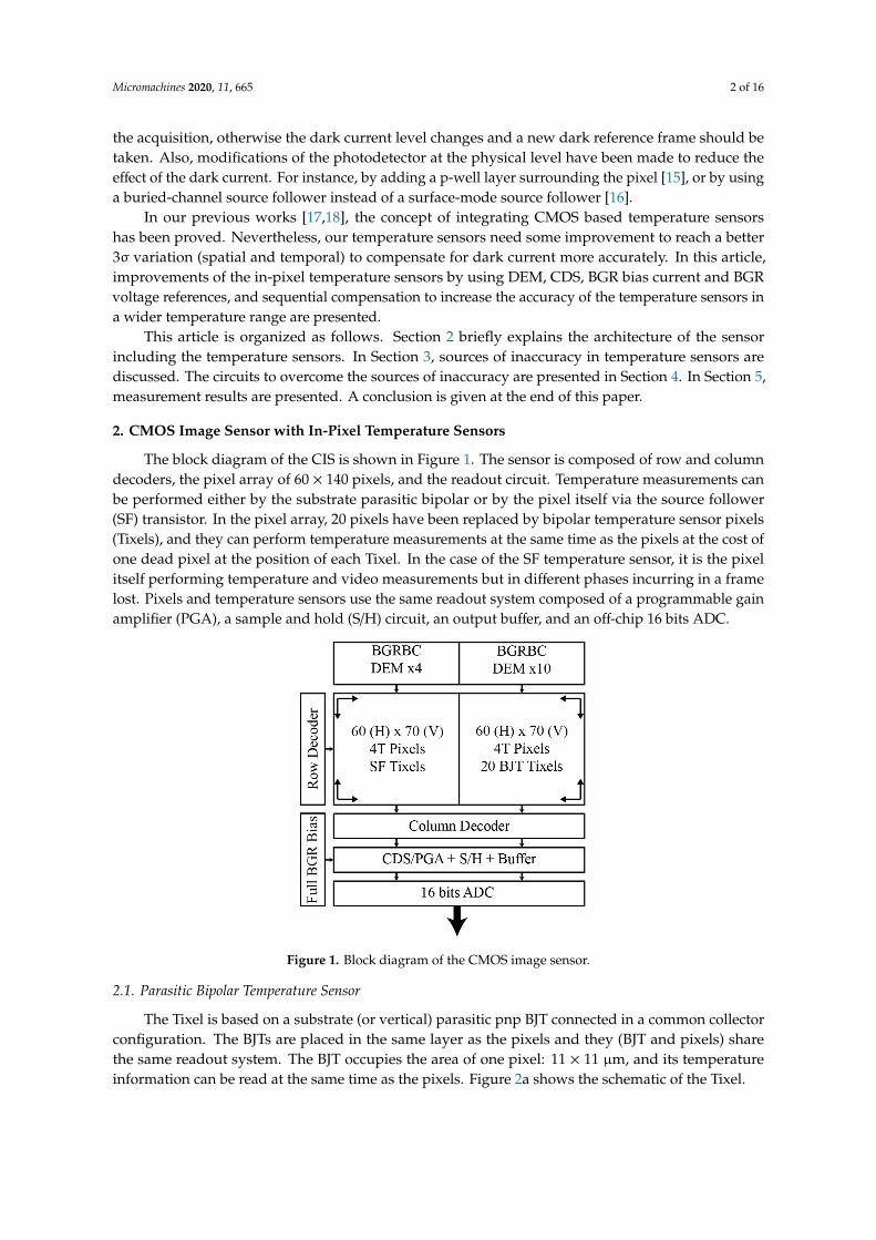
The Tixel is based on a substrate (or vertical) parasitic pnp BJT connected in a common collector configuration. The BJTs are placed in the same layer as the pixels and they (BJT and pixels) share the same readout system. The BJT occupies the area of one pixel: 11 × 11 μm, and its temperature information can be read at the same time as the pixels. Figure 2a shows the schematic of the Tixel.
Figure 1. Block diagram of the CMOS image sensor.
2.1. Parasitic Bipolar Temperature Sensor
The Tixel is based on a substrate (or vertical) parasitic pnp BJT connected in a common collectorconfiguration. The BJTs are placed in the same layer as the pixels and they (BJT and pixels) sharethe same readout system. The BJT occupies the area of one pixel: 11 × 11 µm, and its temperatureinformation can be read at the same time as the pixels. Figure 2a shows the schematic of the Tixel.
Micromachines 2020, 11, 665 3 of 16Micromachines 2020, 11, x FOR PEER REVIEW 3 of 16
(a)
(b)
Figure 2. (a) Schematic of the parasitic substrate BJT based temperature sensor. (b) Schematic of the 4T pixel and the nMOS SF based temperature sensor.
In Figure 2a, Ibias1 and Ibias2 correspond to the bias currents of the BJT, and RS is the row select signal that controls the switches M1 and M2 turning on and off the BJT. The RS signal is the same for Tixels and pixels. Comparing this design to the one in [17], the source follower has been deleted because it added extra non-linearity to the BJT output signal.
To avoid mismatch, only one BJT (instead of two) is used as a temperature sensor. The temperature is obtained via the differential base-emitter voltage (∆ ) when the BJT is biased by two different currents in a ratio :1 (Ibias1 and Ibias2, Ibias2 = ·Ibias1). Equation (1) shows the ∆ which is proportional to absolute temperature (PTAT) [19]: ∆ = ln( ) → = Δ ∙∙ ln( ) (1)
where is the Boltzmann constant, corresponds to the absolute temperature, and is the electric charge. The bias currents are generated by an internal DEM current mirror block and the BGR with temperature independent resistors which provides 1 μA (Section 4.2).
2.2. nMOS Source Follower Temperature Sensor
The nMOS source follower temperature sensor is based on the pixel itself using the SF transistor as a temperature sensor. The size of the pixel is 11 × 11 μm, and Figure 2b shows the schematic of the nMOS SF temperature sensor based on the typical 4T pixel architecture [20,21].
When the pixel is used as a temperature sensor, the following voltage requirements have to be fulfilled: _ + _ , and = _ − , where is the gate voltage of the reset transistor, is the pixel voltage supply, is the threshold voltage of the reset transistor, is the output voltage of the pixel, and is the gate-source voltage of the source follower transistor. Apart of this, the transfer gate (TG) must be switched off to avoid any charge disturbance at the floating diffusion node, and the SF transistor is biased in its subthreshold region where its I-V characteristic follows an exponential-temperature dependent behavior [18]. As in the case of the BJT, the SF temperature sensor is biased (in its subthreshold region) by two different currents in a ratio :1 to obtain the temperature via the differential gate-source voltage (∆ ). Equation (2) shows the ∆ which is PTAT: ∆ = ln( ) → = Δ ∙∙ ln( ) (2)
Figure 2. (a) Schematic of the parasitic substrate BJT based temperature sensor. (b) Schematic of the 4Tpixel and the nMOS SF based temperature sensor.
In Figure 2a, Ibias1 and Ibias2 correspond to the bias currents of the BJT, and RS is the row selectsignal that controls the switches M1 and M2 turning on and off the BJT. The RS signal is the samefor Tixels and pixels. Comparing this design to the one in [17], the source follower has been deletedbecause it added extra non-linearity to the BJT output signal.
To avoid mismatch, only one BJT (instead of two) is used as a temperature sensor. The temperatureis obtained via the differential base-emitter voltage (∆VBE) when the BJT is biased by two differentcurrents in a ratio N:1 (Ibias1 and Ibias2, Ibias2 = N·Ibias1). Equation (1) shows the ∆VBE which isproportional to absolute temperature (PTAT) [19]:
∆VBE =kTq
ln(N)→ T =∆VBE·qk· ln(N)
(1)
where k is the Boltzmann constant, T corresponds to the absolute temperature, and q is the electriccharge. The bias currents are generated by an internal DEM current mirror block and the BGR withtemperature independent resistors which provides 1 µA (Section 4.2).
2.2. nMOS Source Follower Temperature Sensor
The nMOS source follower temperature sensor is based on the pixel itself using the SF transistoras a temperature sensor. The size of the pixel is 11 × 11 µm, and Figure 2b shows the schematic of thenMOS SF temperature sensor based on the typical 4T pixel architecture [20,21].
When the pixel is used as a temperature sensor, the following voltage requirements have to befulfilled: VRST > VPIX_SUP + VTH_RST, and VPIX = VPIX_SUP −VGS, where VRST is the gate voltage ofthe reset transistor, VPIX SUP is the pixel voltage supply, VTH RST is the threshold voltage of the resettransistor, VPIX is the output voltage of the pixel, and VGS is the gate-source voltage of the sourcefollower transistor. Apart of this, the transfer gate (TG) must be switched off to avoid any chargedisturbance at the floating diffusion node, and the SF transistor is biased in its subthreshold regionwhere its I-V characteristic follows an exponential-temperature dependent behavior [18]. As in the caseof the BJT, the SF temperature sensor is biased (in its subthreshold region) by two different currents
Micromachines 2020, 11, 665 4 of 16
in a ratio N:1 to obtain the temperature via the differential gate-source voltage (∆VGS). Equation (2)shows the ∆VGS which is PTAT:
∆VGS = nkTq
ln(N)→ T =∆VGS·q
nk· ln(N)(2)
where n corresponds to a process parameter. As in the case of the Tixel, the biasing currents are alsogenerated by using the DEM block and the BGR providing a unit current of 1 µA.
3. Non-Linearities Affecting the Temperature Sensors
For both based temperature sensors, non-linearities exist that affect the accuracy of the temperaturemeasurement. In this section, the main sources of inaccuracy are presented.
3.1. Sources of Inaccuracies in BJT
As the temperature sensor is formed by only one BJT, it is the base-emitter voltage (VBE) the one ismeasured in every phase to then calculate the PTAT ∆VBE. The VBE is highly influenced by the biascurrent Ibias and the saturation current IS, as shown in Equation (3).
VBE =kTq
ln(
IbiasIS
)(3)
From Equation (3), the influence of Ibias and IS is clear, especially because they are both temperaturedependent [22,23]. The influence of the IS can be trimmed out on a one-point calibration [23]. The biascurrent is usually generated from a well-defined bias voltage utilizing a bias resistor, where the resistoris temperature dependent. To avoid the use of a bias resistor, the design reported here uses a bandgapreference with temperature independent resistors to generate a temperature independent bias current(BGRBC). To reduce the mismatch of the Ibias, one BGRBC circuit is used to supply the DEM currentmirrors. The design of the bias current will be presented in Section 4.
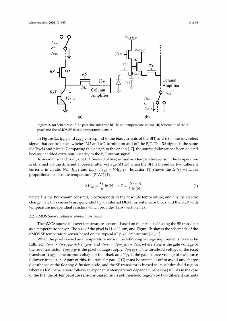
Another source of inaccuracy is the series resistances of the pnp BJT. Figure 3a shows the diodeconnected pnp with series resistances.
Micromachines 2020, 11, x FOR PEER REVIEW 4 of 16
where corresponds to a process parameter. As in the case of the Tixel, the biasing currents are also generated by using the DEM block and the BGR providing a unit current of 1 μA.
3. Non-Linearities Affecting the Temperature Sensors
For both based temperature sensors, non-linearities exist that affect the accuracy of the temperature measurement. In this section, the main sources of inaccuracy are presented.
3.1. Sources of Inaccuracies in BJT
As the temperature sensor is formed by only one BJT, it is the base-emitter voltage ( ) the one is measured in every phase to then calculate the PTAT ∆ . The is highly influenced by the bias current and the saturation current , as shown in Equation (3). = ln (3)
From Equation (3), the influence of and is clear, especially because they are both temperature dependent [22,23]. The influence of the can be trimmed out on a one-point calibration [23]. The bias current is usually generated from a well-defined bias voltage utilizing a bias resistor, where the resistor is temperature dependent. To avoid the use of a bias resistor, the design reported here uses a bandgap reference with temperature independent resistors to generate a temperature independent bias current (BGRBC). To reduce the mismatch of the , one BGRBC circuit is used to supply the DEM current mirrors. The design of the bias current will be presented in Section 4.
Another source of inaccuracy is the series resistances of the pnp BJT. Figure 3a shows the diode connected pnp with series resistances.
(a)
(b)
Figure 3. (a) Diode connected pnp BJT with series resistances. (b) Sequential compensation circuit with effective resistance .
The external of the BJT including the series resistance is shown in Equation (4): = + + = + + + 1 (4)
where corresponds to the intrinsic base-emitter voltage, is the emitter current, is the emitter series resistance, is the base current, is the base series resistance, and corresponds to the current gain. The emitter and base resistances can be modelled as a single series resistance . = + + 1 (5)
Figure 3. (a) Diode connected pnp BJT with series resistances. (b) Sequential compensation circuit witheffective resistance RS.
Micromachines 2020, 11, 665 5 of 16
The external VBE of the BJT including the series resistance is shown in Equation (4):
VBE = VB′E′ + IERE + IBRB = VB′E′ + IE
(RE +
RB
βF + 1
)(4)
where VB′E′ corresponds to the intrinsic base-emitter voltage, IE is the emitter current, RE is the emitterseries resistance, IB is the base current, RB is the base series resistance, and βF corresponds to the currentgain. The emitter and base resistances can be modelled as a single series resistance RS.
RS = RE +RB
βF + 1(5)
The effect of the temperature dependent βF on RS can be reduced by selecting the rightemitter-current (bias current) range where the βF is current independent [23]. Therefore, an accuratePTAT differential base-emitter voltage can be generated by a well-defined emitter-current ratio (resultingin a well-defined collector-current ratio as well) where βF is independent of the Ibias in the selectedtemperature range. Also, the use of a wide base helps to reduce the non-idealities that result in acurrent-dependent βF (for instance, small diffusion current injected from the base into the emitter.)
Ignoring the effect of the current gain, the base-emitter voltage can be expressed as:
VBE =kTq
ln(
IbiasIS
)+ IbiasRS (6)
and the differential base-emitter voltage.
∆VBE =kTq
ln(N) + Ibias(N − 1)RS (7)
From Equations (6) and (7), it is clear that the bias current and the series resistance affect thelinearity of the VBE and ∆VBE. To cancel the effect of RS a sequential compensation is applied by usingEquation (8) [23,24]:
NiNi − 1
VBE(Ibias) −1
Ni − 1VBE(Ni·Ibias) =
kTq
ln(
IbiasIS
)−
1Ni − 1
kTq
ln(Ni) (8)
where Ni corresponds to the number of bias currents. To generate a ∆VBE where the RS is cancelled,the BJT is biased by three bias currents, as shown in Figure 3b. For example, if N1 = 3 and N2 = 9,then the differential base-emitter voltage is represented by:
4·VBE(3Ibias) − 3·VBE(Ibias) −VBE(9Ibias) =kTq
ln(9) (9)
Equation (9) shows that the series resistance has been cancelled by using sequential compensation.
3.2. Sources of Inaccuracies in nMOS SF
When the nMOS source followerbased temperature sensor is biased in the subthreshold region,the gate-source voltage VGS follows Equation (10) [18]:
VGS = nkTq
ln(
IbiasIDS
)−VTH (10)
where IDS is the saturation current, and VTH corresponds to the threshold voltage of the source followertransistor. As in the case of the BJT, the bias current and the saturation current have an impact onthe value of VGS, but also the threshold voltage. The VTH is minimized when the SF is biased with
Micromachines 2020, 11, 665 6 of 16
ratiometric currents to obtain the differential gate-source voltage. The variation of IDS leads to acorrection of a one-point calibration, while an accurate Ibias will be shown in Section 4.2.
A technique to diminish the effect of the factor n, the dimensions W/L of each SF transistor, and thevariation of IDS was proposed in [18]. All the pixels in one column are biased to increase the total areaof the SF temperature sensor to mimic a larger parallel device with their gates and sources connectedto the voltage supply and the output, respectively. A larger device suffers less from process variations.Other consequences of this technique are the reduction of the output noise of the pixel (includingthermal and flicker noise). However, this technique has as a drawback that the temperature is notmeasured locally per pixel but per column. In this paper instead, a large enough bias current has beenused to reduce the effect of n and IDS but sufficiently small to not incur in mismatch problems of the SFtemperature sensor. This technique was proposed in [25].
3.3. Sources of Inaccuracies of the Readout System
The column amplifier suffers from thermal noise because all its components are temperaturedependent. One way to compensate for this temperature dependence is to change all the biasing of theamplifier by bandgap references. Another source of inaccuracy is the reference voltage of the amplifier.If the reference is temperature dependent, then the output signal is also affected when the temperaturechanges. The reference voltage has been changed by an internal BGR. The architecture of the BGR biasvoltage and reference voltage is explained in Section 4.
Also, the column amplifier has an offset produced by the mismatch of the inner transistors thatcan be cancelled by using CDS.
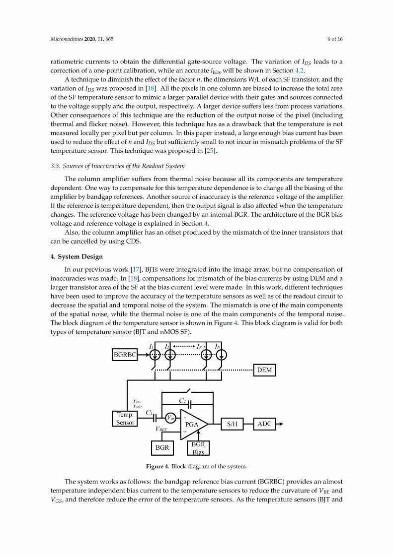
4. System Design
In our previous work [17], BJTs were integrated into the image array, but no compensation ofinaccuracies was made. In [18], compensations for mismatch of the bias currents by using DEM and alarger transistor area of the SF at the bias current level were made. In this work, different techniqueshave been used to improve the accuracy of the temperature sensors as well as of the readout circuit todecrease the spatial and temporal noise of the system. The mismatch is one of the main componentsof the spatial noise, while the thermal noise is one of the main components of the temporal noise.The block diagram of the temperature sensor is shown in Figure 4. This block diagram is valid for bothtypes of temperature sensor (BJT and nMOS SF).
Micromachines 2020, 11, x FOR PEER REVIEW 6 of 16
3.3. Sources of Inaccuracies of the Readout System
The column amplifier suffers from thermal noise because all its components are temperature dependent. One way to compensate for this temperature dependence is to change all the biasing of the amplifier by bandgap references. Another source of inaccuracy is the reference voltage of the amplifier. If the reference is temperature dependent, then the output signal is also affected when the temperature changes. The reference voltage has been changed by an internal BGR. The architecture of the BGR bias voltage and reference voltage is explained in Section 4.
Also, the column amplifier has an offset produced by the mismatch of the inner transistors that can be cancelled by using CDS.
4. System Design
In our previous work [17], BJTs were integrated into the image array, but no compensation of inaccuracies was made. In [18], compensations for mismatch of the bias currents by using DEM and a larger transistor area of the SF at the bias current level were made. In this work, different techniques have been used to improve the accuracy of the temperature sensors as well as of the readout circuit to decrease the spatial and temporal noise of the system. The mismatch is one of the main components of the spatial noise, while the thermal noise is one of the main components of the temporal noise. The block diagram of the temperature sensor is shown in Figure 4. This block diagram is valid for both types of temperature sensor (BJT and nMOS SF).
Figure 4. Block diagram of the system.
The system works as follows: the bandgap reference bias current (BGRBC) provides an almost temperature independent bias current to the temperature sensors to reduce the curvature of and
, and therefore reduce the error of the temperature sensors. As the temperature sensors (BJT and nMOS SF) measure the temperature via the PTAT differential voltage, they need to be biased by two different currents in a ratio : 1. The current mirror composed of currents I1 to IN provides the current ratio for the temperature sensors. However, due to mismatch, the ratio is not exactly : 1 which leads to an error when comparing different temperature sensors of the same chip. The mismatch is cancelled by using dynamic element matching which averages the total current provided to the temperature sensor. By using DEM, the mismatch error can be reduced by at least one order of magnitude [23]. The output of the temperature sensor is read by a programmable gain amplifier (PGA), where a gain is applied. The PGA suffers from an offset voltage (VOS) due to the mismatch of the inner transistors of the amplifier. To cancel the VOS, correlated double sampling (CDS) is applied by using the PGA and the sample and hold (S/H) circuit. Taking the BJT as an example, in one phase, the output voltage is stored in and the offset plus the reference voltage ( + ) are sampled and stored in an analog memory in the S/H circuit. Then, in the next phase the output signal of the temperature sensor is stored in , obtaining the differential base-emitter voltage (Δ =− ) which is amplified by the gain = / and stored with ( + ) in another analog
Figure 4. Block diagram of the system.
The system works as follows: the bandgap reference bias current (BGRBC) provides an almosttemperature independent bias current to the temperature sensors to reduce the curvature of VBE andVGS, and therefore reduce the error of the temperature sensors. As the temperature sensors (BJT and
Micromachines 2020, 11, 665 7 of 16
nMOS SF) measure the temperature via the PTAT differential voltage, they need to be biased by twodifferent currents in a ratio N : 1. The current mirror composed of currents I1 to IN provides the currentratio for the temperature sensors. However, due to mismatch, the ratio is not exactly N : 1 which leadsto an error when comparing different temperature sensors of the same chip. The mismatch is cancelledby using dynamic element matching which averages the total current provided to the temperaturesensor. By using DEM, the mismatch error can be reduced by at least one order of magnitude [23].The output of the temperature sensor is read by a programmable gain amplifier (PGA), where a gain isapplied. The PGA suffers from an offset voltage (VOS) due to the mismatch of the inner transistorsof the amplifier. To cancel the VOS, correlated double sampling (CDS) is applied by using the PGAand the sample and hold (S/H) circuit. Taking the BJT as an example, in one phase, the output voltageVBE1 is stored in C1 and the offset plus the reference voltage (VOS + VREF) are sampled and stored inan analog memory in the S/H circuit. Then, in the next phase the output signal of the temperaturesensor VBE2 is stored in C1, obtaining the differential base-emitter voltage (∆VBE = VBE2 −VBE1) whichis amplified by the gain A = C1/C2 and stored with (VOS + VREF) in another analog memory in theS/H circuit. In this way, subtracting the stored values in both analog memories the offset is cancelled:Vout = (A·∆VBE + VREF + VOS) − (VREF + VOS) = A·∆VBE.
To reduce the thermal noise of the PGA, bandgap references have been used to bias the PGA andfor the reference voltage. In Section 4.3, comparison between using the biasing of [17] and the BGRbias will be shown.
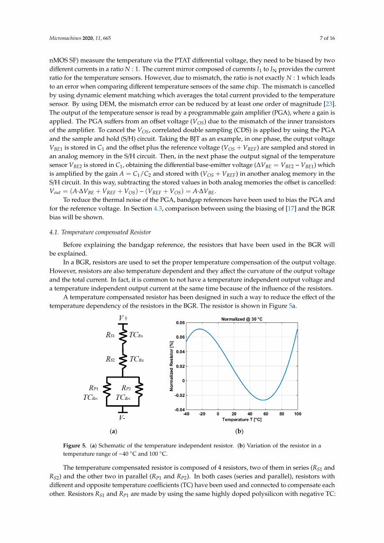
4.1. Temperature compensated Resistor
Before explaining the bandgap reference, the resistors that have been used in the BGR willbe explained.
In a BGR, resistors are used to set the proper temperature compensation of the output voltage.However, resistors are also temperature dependent and they affect the curvature of the output voltageand the total current. In fact, it is common to not have a temperature independent output voltage anda temperature independent output current at the same time because of the influence of the resistors.
A temperature compensated resistor has been designed in such a way to reduce the effect of thetemperature dependency of the resistors in the BGR. The resistor is shown in Figure 5a.
Micromachines 2020, 11, x FOR PEER REVIEW 7 of 16
memory in the S/H circuit. In this way, subtracting the stored values in both analog memories the offset is cancelled: = ( Δ + + ) − ( + ) = Δ .
To reduce the thermal noise of the PGA, bandgap references have been used to bias the PGA and for the reference voltage. In Section 4.3, comparison between using the biasing of [17] and the BGR bias will be shown.
4.1. Temperature compensated Resistor
Before explaining the bandgap reference, the resistors that have been used in the BGR will be explained.
In a BGR, resistors are used to set the proper temperature compensation of the output voltage. However, resistors are also temperature dependent and they affect the curvature of the output voltage and the total current. In fact, it is common to not have a temperature independent output voltage and a temperature independent output current at the same time because of the influence of the resistors.
A temperature compensated resistor has been designed in such a way to reduce the effect of the temperature dependency of the resistors in the BGR. The resistor is shown in Figure 5a.
(a)
(b)
Figure 5. (a) Schematic of the temperature independent resistor. (b) Variation of the resistor in a temperature range of -40 °C and 100 °C.
The temperature compensated resistor is composed of 4 resistors, two of them in series ( and ) and the other two in parallel ( and ). In both cases (series and parallel), resistors with
different and opposite temperature coefficients (TC) have been used and connected to compensate each other. Resistors and are made by using the same highly doped polysilicon with negative TC: and , respectively (where = ). Resistors and correspond to the same lowly doped polysilicon resistor with positive TC: and , respectively (where = ). The total resistance ( ) and the total TC are shown in Equations (11) and (12), respectively: = + + + (11)
= 0 = + + +( + ) . (12)
Treating the series and the parallel resistors separately, the value of the resistors can be chosen by Equations (13) and (14): = (13)
Figure 5. (a) Schematic of the temperature independent resistor. (b) Variation of the resistor in atemperature range of −40 C and 100 C.
The temperature compensated resistor is composed of 4 resistors, two of them in series (RS1 andRS2) and the other two in parallel (RP1 and RP2). In both cases (series and parallel), resistors withdifferent and opposite temperature coefficients (TC) have been used and connected to compensate eachother. Resistors RS1 and RP1 are made by using the same highly doped polysilicon with negative TC:
Micromachines 2020, 11, 665 8 of 16
TCRS1 and TCRP1 , respectively (where TCRS2 = TCRP2). Resistors RS2 and RP2 correspond to the samelowly doped polysilicon resistor with positive TC: TCRS2 and TCRP2 , respectively (where TCRS2 = TCRP2 ).The total resistance (RT) and the total TC are shown in Equations (11) and (12), respectively:
RT = RS1 + RS2 +RP1RP2
RP1 + RP2(11)
∂RT
∂T= 0 = RS1TCRS1 + RS2TCRS2 +
RP1RP2(RP1TCRP2 + RP2TCRP1
)(RP1 + RP2)
2 (12)
Treating the series and the parallel resistors separately, the value of the resistors can be chosen byEquations (13) and (14):
RS1
RS2=
TCRS2
TCRS1
(13)
RP1
RP2=
TCRP1
TCRP2
(14)
The curvature of the resistors in series is convex and the curvature of the resistors in parallel isconcave. Combining both curvatures, the variation of the resistance results in a TC of 0.085 ppm/C,as shown in Figure 5b.
4.2. Bandgap Reference with Temperature Compensated Resistors
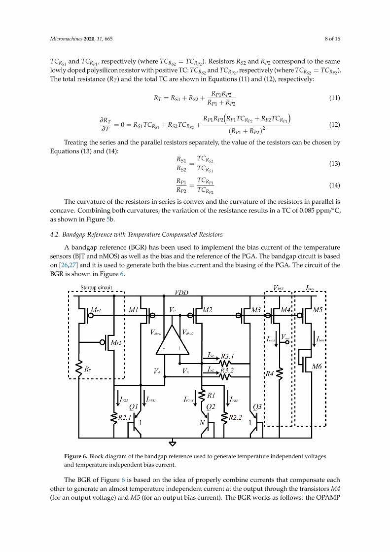
A bandgap reference (BGR) has been used to implement the bias current of the temperaturesensors (BJT and nMOS) as well as the bias and the reference of the PGA. The bandgap circuit is basedon [26,27] and it is used to generate both the bias current and the biasing of the PGA. The circuit of theBGR is shown in Figure 6.
Micromachines 2020, 11, x FOR PEER REVIEW 8 of 16
= . (14)
The curvature of the resistors in series is convex and the curvature of the resistors in parallel is concave. Combining both curvatures, the variation of the resistance results in a TC of 0.085 ppm/°C, as shown in Figure 5b.
4.2. Bandgap Reference with Temperature Compensated Resistors
A bandgap reference (BGR) has been used to implement the bias current of the temperature sensors (BJT and nMOS) as well as the bias and the reference of the PGA. The bandgap circuit is based on [26,27] and it is used to generate both the bias current and the biasing of the PGA. The circuit of the BGR is shown in Figure 6.
Figure 6. Block diagram of the bandgap reference used to generate temperature independent voltages and temperature independent bias current.
The BGR of Figure 6 is based on the idea of properly combine currents that compensate each other to generate an almost temperature independent current at the output through the transistors M4 (for an output voltage) and M5 (for an output bias current). The BGR works as follows: the OPAMP forces voltages and to be equal, this results in equal currents through transistors M1 and M2. Transistors Q2 and Q1 have an emitter area ratio of N, generating a differential base-emitter voltage (∆ ) resulting in a PTAT current in 1. As resistors 2.1 and 2.2 are nominally identical, a current in 2.1 (and 2.2) ( ) that is proportional to the base emitter-voltage of Q1 (and Q2) is generated. The current is proportional to the differential base-emitter voltage between Q1 and Q3 in 3.1 ( 3.1 = 3.2). Currents and are used to compensate first order and higher order non-linearities of , respectively. Therefore, the total current in transistor M4 is (for simplicity 2.1 = 2.2 = 2, and 3.1 = 3.2 = 3): = + + = 2 + ∆ 1 + −3 (15)
where the value of depends on the temperature behavior of resistors 1_3. This is the reason why the temperature compensated resistor of Section 4.1 is used.
Figure 6. Block diagram of the bandgap reference used to generate temperature independent voltagesand temperature independent bias current.
The BGR of Figure 6 is based on the idea of properly combine currents that compensate eachother to generate an almost temperature independent current at the output through the transistors M4(for an output voltage) and M5 (for an output bias current). The BGR works as follows: the OPAMP
Micromachines 2020, 11, 665 9 of 16
forces voltages VA and VB to be equal, this results in equal currents through transistors M1 and M2.Transistors Q2 and Q1 have an emitter area ratio of N, generating a differential base-emitter voltage(∆VBE) resulting in a PTAT current IPTAT in R1. As resistors R2.1 and R2.2 are nominally identical,a current in R2.1 (and R2.2 ) (IVBE) that is proportional to the base emitter-voltage of Q1 (and Q2) isgenerated. The current INL is proportional to the differential base-emitter voltage between Q1 andQ3 in R3.1 (R3.1 = R3.2). Currents IPTAT and INL are used to compensate first order and higher ordernon-linearities of IVBE, respectively. Therefore, the total current Itotal in transistor M4 is (for simplicityR2.1 = R2.2 = R2, and R3.1 = R3.2 = R3):
Itotal = IVBE + IPTAT + INL =VBE
R2+
∆VBE
R1+
VBEQ1 −VBEQ3
R3(15)
where the value of Itotal depends on the temperature behavior of resistors R1_3. This is the reason whythe temperature compensated resistor of Section 4.1 is used.
This total current is almost temperature independent which leads to a temperature independentoutput voltage as well. The output voltage Vout and its temperature coefficient are shown in Equations(16) and (17), respectively:
Vout = R4·Itotal = R4(
VBEQ1
R2+
∆VBE
R1+
VBEQ1 −VBEQ3
R3
)(16)
∂Vout
∂T= 0 = R4
1
R2∂VBEQ1
∂T+
1R1
∂∆VBE
∂T︸ ︷︷ ︸f irst order
+1
R3
∂(VBEQ1 −VBEQ3
)∂T︸ ︷︷ ︸
higher order
(17)
Treating the first order TC and higher order TC of Equation (17) separately, the first ordernon-linearity is compensated by properly choosing the values of R1, R2, and N, satisfying Equation (18):
0 = 1R2
∂VBEQ1∂T + 1
R1∂∆VBE∂T = 1
R2 TCVBEQ1 +1
R1kq ln(N)
=⇒ R2R1 ln(N) =
qk TCVBE = 23.22
(18)
where TCVBEQ1 is the temperature coefficient of VBEQ1 being close to –2 mV/C.On the other hand, the base-emitter voltage of a bipolar transistor can be also expressed as [28]:
VBE(T) = VBG − (VBG −VBE0)TT0− (η− α)VT ln
(TT0
)(19)
where VBG is the bandgap voltage of silicon, VBE0 corresponds to the base-emitter voltage at roomtemperature, T0 corresponds to room temperature, η is a temperature constant dependent on technology(for bipolar is around 4), α corresponds to the temperature dependence of the collector current (equalto 1 if the current is PTAT and equal to 0 if the current is temperature independent [26]), and VT is thethermal voltage equal to kT/q. The current INL can be expressed by using Equation (20):
INL =VBEQ1 −VBEQ3
R3=
VT ln(
TT0
)R3
(20)
and the value of R3 can be chosen by comparing Equations (16), (19), and using (20) [26]:
R3 =R2η− 1
(21)
The value of the resistors R1, R2, and R3 can be properly chosen by using Equations (18) and (21).The emitter area ratio of N is equal to 23, R1 = 50 kΩ, R2 = 400 kΩ, η is 4, and R3 = 135 kΩ.
Micromachines 2020, 11, 665 10 of 16
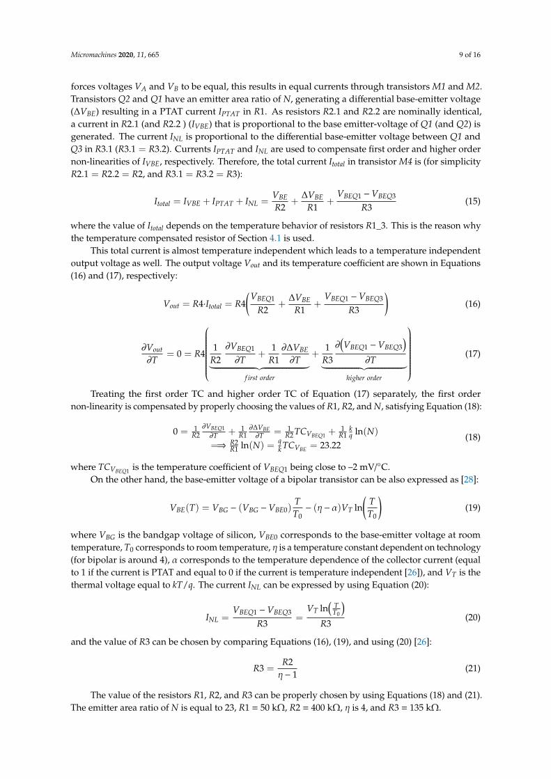
4.3. Post-Layout Simulations of the BGR Current and Voltages
The bias current is generated by properly scaling transistor M5 in the BGR, in this way the biascurrent is: Ibias = Itotal/ W
L , where W/L is the size of transistor M5. Post-layout simulation shows thatthe BGRBC provides an almost constant current of 1 µA and an accuracy of 61.87 ppm/C in thetemperature range of −40 C and 100 C as shown in Figure 7a.Micromachines 2020, 11, x FOR PEER REVIEW 10 of 16
(a) (b)
Figure 7. (a) Simulation of the BGR bias current of the temperature sensors. (b) Monte Carlo analysis of the bandgap reference bias current.
ge 7b shows the Monte Carlo analysis of the BGR bias current. The analysis was done by running 500 simulation where the process and mismatch of all components of the BGR where analysed. Results show a very stable BGR with a variation of 9% from the mean value at 100 °C (worst case).
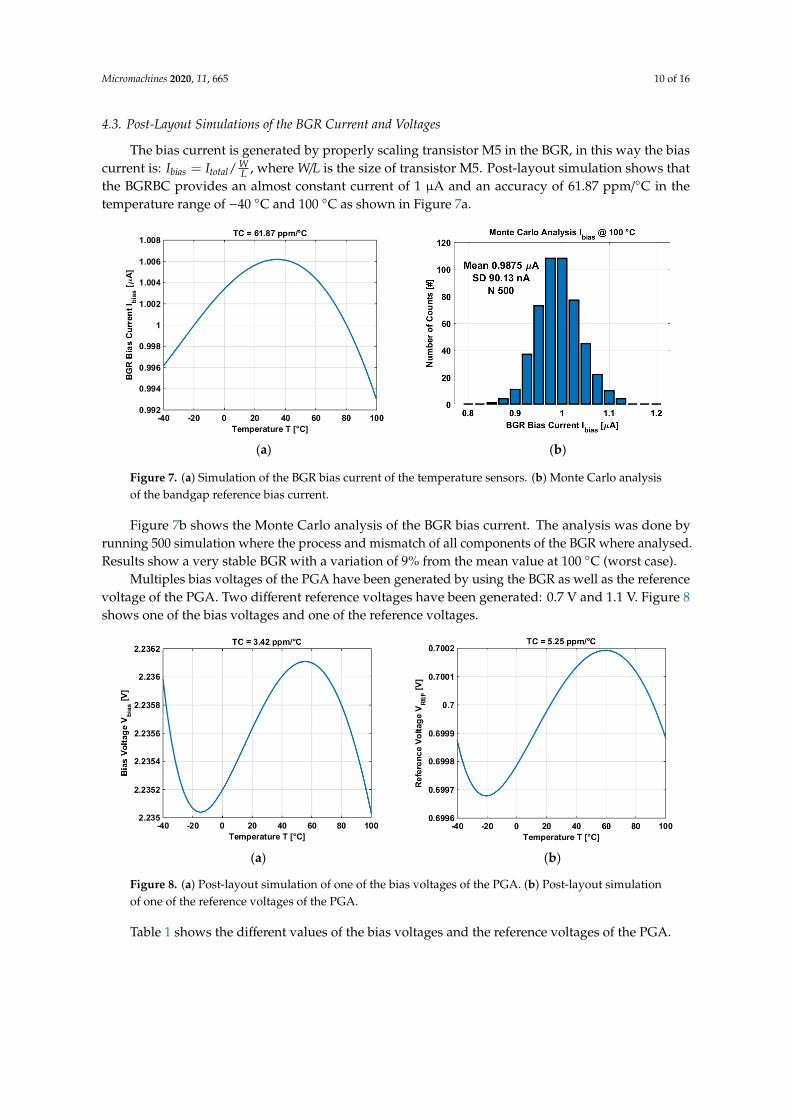
Multiples bias voltages of the PGA have been generated by using the BGR as well as the reference voltage of the PGA. Two different reference voltages have been generated: 0.7 V and 1.1 V. Figure 8 shows one of the bias voltages and one of the reference voltages.
(a) (b)
Figure 8. (a) Post-layout simulation of one of the bias voltages of the PGA. (b) Post-layout simulation of one of the reference voltages of the PGA.
Table 1 shows the different values of the bias voltages and the reference voltages of the PGA.
Table 1. Temperature coefficient and power consumption of the different bias voltages and the reference voltages used in the PGA.
Voltage [V] TC [ppm/°C] Power Consumption @ 25 °C [μW] 2.2 (VBias) 3.4239 56 1.1 (VBias) 3.6959 54 0.9 (VBias) 4.3051 52 1.1 (VREF) 3.4406 54 0.7 (VREF) 5.2471 54
A comparison between using the bias of the PGA in [17] and the bias based on the BGR is shown in Figure 9.
Figure 7. (a) Simulation of the BGR bias current of the temperature sensors. (b) Monte Carlo analysisof the bandgap reference bias current.
Figure 7b shows the Monte Carlo analysis of the BGR bias current. The analysis was done byrunning 500 simulation where the process and mismatch of all components of the BGR where analysed.Results show a very stable BGR with a variation of 9% from the mean value at 100 C (worst case).
Multiples bias voltages of the PGA have been generated by using the BGR as well as the referencevoltage of the PGA. Two different reference voltages have been generated: 0.7 V and 1.1 V. Figure 8shows one of the bias voltages and one of the reference voltages.
Micromachines 2020, 11, x FOR PEER REVIEW 10 of 16
(a) (b)
Figure 7. (a) Simulation of the BGR bias current of the temperature sensors. (b) Monte Carlo analysis
of the bandgap reference bias current.
Figure 7b shows the Monte Carlo analysis of the BGR bias current. The analysis was done by
running 500 simulation where the process and mismatch of all components of the BGR where
analysed. Results show a very stable BGR with a variation of 9% from the mean value at 100 °C (worst
case).
Multiples bias voltages of the PGA have been generated by using the BGR as well as the
reference voltage of the PGA. Two different reference voltages have been generated: 0.7 V and 1.1 V.
Figure 8 shows one of the bias voltages and one of the reference voltages.
(a) (b)
Figure 8. (a) Post-layout simulation of one of the bias voltages of the PGA. (b) Post-layout simulation
of one of the reference voltages of the PGA.
Table 1 shows the different values of the bias voltages and the reference voltages of the PGA.
Table 1. Temperature coefficient and power consumption of the different bias voltages and the
reference voltages used in the PGA.
Voltage [V] TC [ppm/°C] Power Consumption @ 25 °C [μW]
2.2 (VBias) 3.4239 56
1.1 (VBias) 3.6959 54
0.9 (VBias) 4.3051 52
1.1 (VREF) 3.4406 54
0.7 (VREF) 5.2471 54
A comparison between using the bias of the PGA in [17] and the bias based on the BGR is shown
in Figure 9.
Figure 8. (a) Post-layout simulation of one of the bias voltages of the PGA. (b) Post-layout simulationof one of the reference voltages of the PGA.
Table 1 shows the different values of the bias voltages and the reference voltages of the PGA.
Micromachines 2020, 11, 665 11 of 16
Table 1. Temperature coefficient and power consumption of the different bias voltages and the referencevoltages used in the PGA.
Voltage [V] TC [ppm/C] Power Consumption @ 25 C [µW]
2.2 (VBias) 3.4239 561.1 (VBias) 3.6959 540.9 (VBias) 4.3051 521.1 (VREF) 3.4406 540.7 (VREF) 5.2471 54
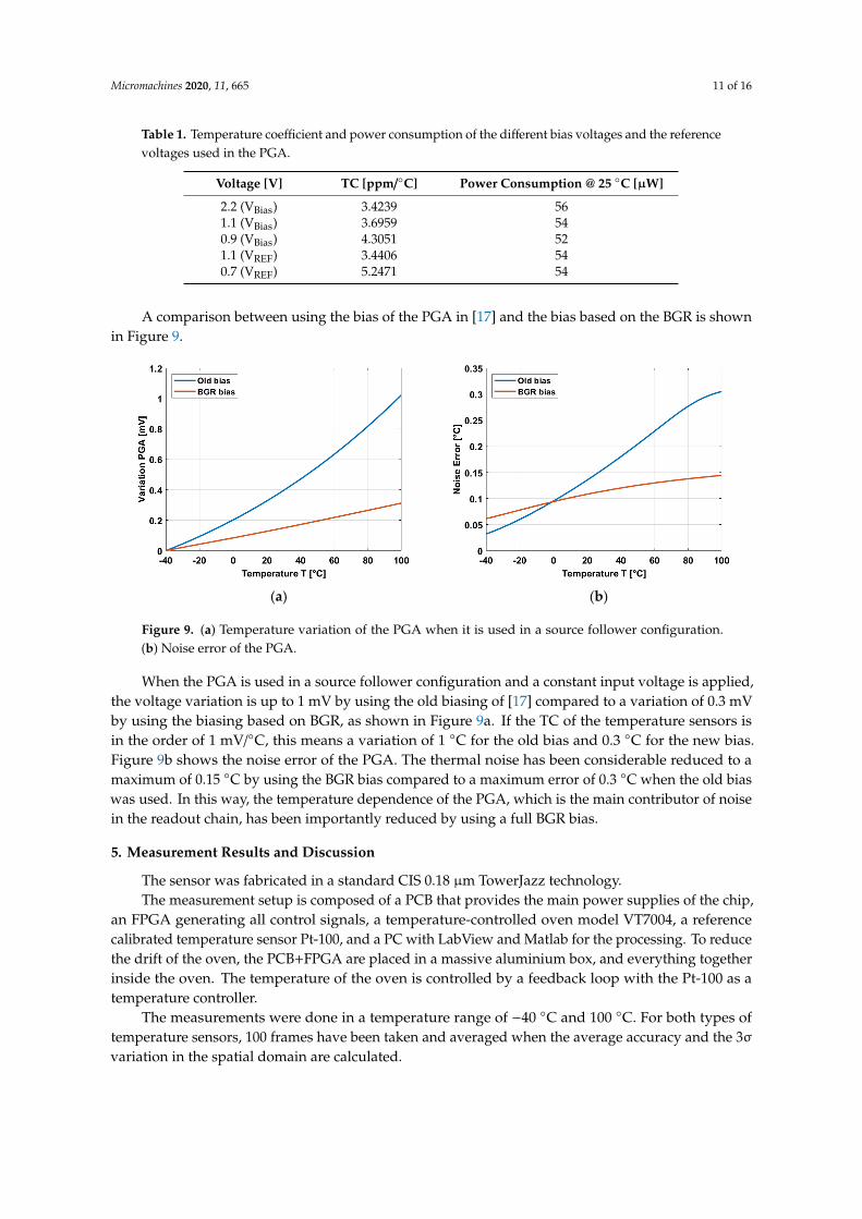
A comparison between using the bias of the PGA in [17] and the bias based on the BGR is shownin Figure 9.
Micromachines 2020, 11, x FOR PEER REVIEW 11 of 16
(a) (b)
Figure 9. (a) Temperature variation of the PGA when it is used in a source follower configuration. (b) Noise error of the PGA.
When the PGA is used in a source follower configuration and a constant input voltage is applied, the voltage variation is up to 1 mV by using the old biasing of [17] compared to a variation of 0.3 mV by using the biasing based on BGR, as shown in Figure 9a. If the TC of the temperature sensors is in the order of 1 mV/°C, this means a variation of 1 °C for the old bias and 0.3 °C for the new bias. Figure 9b shows the noise error of the PGA. The thermal noise has been considerable reduced to a maximum of 0.15 °C by using the BGR bias compared to a maximum error of 0.3 °C when the old bias was used. In this way, the temperature dependence of the PGA, which is the main contributor of noise in the readout chain, has been importantly reduced by using a full BGR bias.
5. Measurement Results and Discussion
The sensor was fabricated in a standard CIS 0.18 μm TowerJazz technology. The measurement setup is composed of a PCB that provides the main power supplies of the
chip, an FPGA generating all control signals, a temperature-controlled oven model VT7004, a reference calibrated temperature sensor Pt-100, and a PC with LabView and Matlab for the processing. To reduce the drift of the oven, the PCB+FPGA are placed in a massive aluminium box, and everything together inside the oven. The temperature of the oven is controlled by a feedback loop with the Pt-100 as a temperature controller.
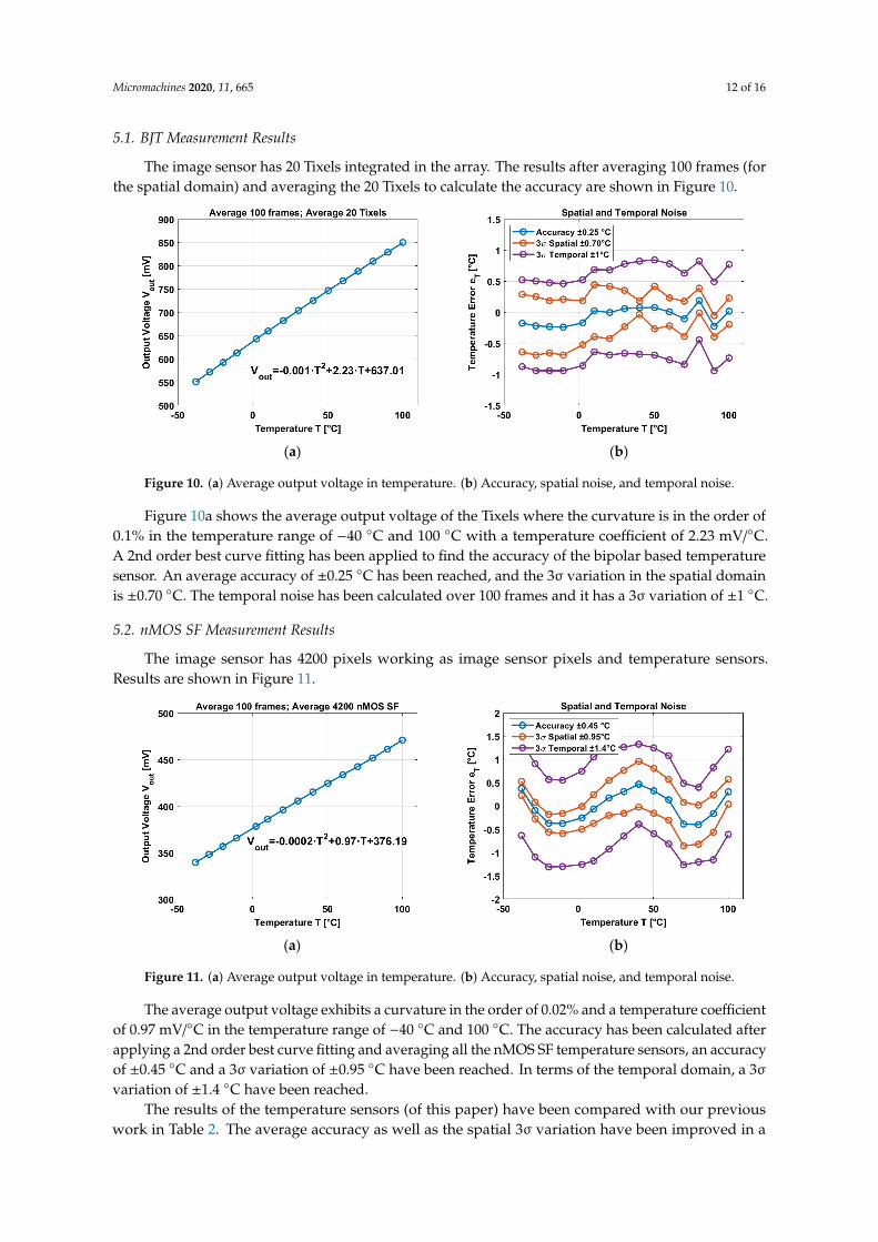
The measurements were done in a temperature range of −40 °C and 100 °C. For both types of temperature sensors, 100 frames have been taken and averaged when the average accuracy and the 3σ variation in the spatial domain are calculated.
5.1. BJT Measurement Results
The image sensor has 20 Tixels integrated in the array. The results after averaging 100 frames (for the spatial domain) and averaging the 20 Tixels to calculate the accuracy are shown in Figure 10.
Figure 9. (a) Temperature variation of the PGA when it is used in a source follower configuration.(b) Noise error of the PGA.
When the PGA is used in a source follower configuration and a constant input voltage is applied,the voltage variation is up to 1 mV by using the old biasing of [17] compared to a variation of 0.3 mVby using the biasing based on BGR, as shown in Figure 9a. If the TC of the temperature sensors isin the order of 1 mV/C, this means a variation of 1 C for the old bias and 0.3 C for the new bias.Figure 9b shows the noise error of the PGA. The thermal noise has been considerable reduced to amaximum of 0.15 C by using the BGR bias compared to a maximum error of 0.3 C when the old biaswas used. In this way, the temperature dependence of the PGA, which is the main contributor of noisein the readout chain, has been importantly reduced by using a full BGR bias.
5. Measurement Results and Discussion
The sensor was fabricated in a standard CIS 0.18 µm TowerJazz technology.The measurement setup is composed of a PCB that provides the main power supplies of the chip,
an FPGA generating all control signals, a temperature-controlled oven model VT7004, a referencecalibrated temperature sensor Pt-100, and a PC with LabView and Matlab for the processing. To reducethe drift of the oven, the PCB+FPGA are placed in a massive aluminium box, and everything togetherinside the oven. The temperature of the oven is controlled by a feedback loop with the Pt-100 as atemperature controller.
The measurements were done in a temperature range of −40 C and 100 C. For both types oftemperature sensors, 100 frames have been taken and averaged when the average accuracy and the 3σvariation in the spatial domain are calculated.
Micromachines 2020, 11, 665 12 of 16
5.1. BJT Measurement Results
The image sensor has 20 Tixels integrated in the array. The results after averaging 100 frames (forthe spatial domain) and averaging the 20 Tixels to calculate the accuracy are shown in Figure 10.
Micromachines 2020, 11, x FOR PEER REVIEW 12 of 16
(a) (b)
Figure 10. (a) Average output voltage in temperature. (b) Accuracy, spatial noise, and temporal noise.
Figure 10a shows the average output voltage of the Tixels where the curvature is in the order of 0.1% in the temperature range of −40 °C and 100 °C with a temperature coefficient of 2.23 mV/°C. A 2nd order best curve fitting has been applied to find the accuracy of the bipolar based temperature sensor. An average accuracy of ±0.25 °C has been reached, and the 3σ variation in the spatial domain is ±0.70 °C. The temporal noise has been calculated over 100 frames and it has a 3σ variation of ±1 °C.
5.2. nMOS SF Measurement Results
The image sensor has 4200 pixels working as image sensor pixels and temperature sensors. Results are shown in Figure 11.
(a) (b)
Figure 11. (a) Average output voltage in temperature. (b) Accuracy, spatial noise, and temporal noise.
The average output voltage exhibits a curvature in the order of 0.02% and a temperature coefficient of 0.97 mV/°C in the temperature range of −40 °C and 100 °C. The accuracy has been calculated after applying a 2nd order best curve fitting and averaging all the nMOS SF temperature sensors, an accuracy of ±0.45 °C and a 3σ variation of ±0.95 °C have been reached. In terms of the temporal domain, a 3σ variation of ±1.4 °C have been reached.
The results of the temperature sensors (of this paper) have been compared with our previous work in Table 2. The average accuracy as well as the spatial 3σ variation have been improved in a wider temperature range compared to [17] thanks to the use of the different techniques applying in this design. The advantages of the temperature sensors of this work are a small area, good untrimmed average accuracy and spatial 3σ variation, and a wide temperature range.
Figure 10. (a) Average output voltage in temperature. (b) Accuracy, spatial noise, and temporal noise.
Figure 10a shows the average output voltage of the Tixels where the curvature is in the order of0.1% in the temperature range of −40 C and 100 C with a temperature coefficient of 2.23 mV/C.A 2nd order best curve fitting has been applied to find the accuracy of the bipolar based temperaturesensor. An average accuracy of ±0.25 C has been reached, and the 3σ variation in the spatial domainis ±0.70 C. The temporal noise has been calculated over 100 frames and it has a 3σ variation of ±1 C.
5.2. nMOS SF Measurement Results
The image sensor has 4200 pixels working as image sensor pixels and temperature sensors.Results are shown in Figure 11.
Micromachines 2020, 11, x FOR PEER REVIEW 12 of 16
(a) (b)
Figure 10. (a) Average output voltage in temperature. (b) Accuracy, spatial noise, and temporal noise.
Figure 10a shows the average output voltage of the Tixels where the curvature is in the order of 0.1% in the temperature range of −40 °C and 100 °C with a temperature coefficient of 2.23 mV/°C. A 2nd order best curve fitting has been applied to find the accuracy of the bipolar based temperature sensor. An average accuracy of ±0.25 °C has been reached, and the 3σ variation in the spatial domain is ±0.70 °C. The temporal noise has been calculated over 100 frames and it has a 3σ variation of ±1 °C.
5.2. nMOS SF Measurement Results
The image sensor has 4200 pixels working as image sensor pixels and temperature sensors. Results are shown in Figure 11.
(a) (b)
Figure 11. (a) Average output voltage in temperature. (b) Accuracy, spatial noise, and temporal noise.
The average output voltage exhibits a curvature in the order of 0.02% and a temperature coefficient of 0.97 mV/°C in the temperature range of −40 °C and 100 °C. The accuracy has been calculated after applying a 2nd order best curve fitting and averaging all the nMOS SF temperature sensors, an accuracy of ±0.45 °C and a 3σ variation of ±0.95 °C have been reached. In terms of the temporal domain, a 3σ variation of ±1.4 °C have been reached.
The results of the temperature sensors (of this paper) have been compared with our previous work in Table 2. The average accuracy as well as the spatial 3σ variation have been improved in a wider temperature range compared to [17] thanks to the use of the different techniques applying in this design. The advantages of the temperature sensors of this work are a small area, good untrimmed average accuracy and spatial 3σ variation, and a wide temperature range.
Figure 11. (a) Average output voltage in temperature. (b) Accuracy, spatial noise, and temporal noise.
The average output voltage exhibits a curvature in the order of 0.02% and a temperature coefficientof 0.97 mV/C in the temperature range of −40 C and 100 C. The accuracy has been calculated afterapplying a 2nd order best curve fitting and averaging all the nMOS SF temperature sensors, an accuracyof ±0.45 C and a 3σ variation of ±0.95 C have been reached. In terms of the temporal domain, a 3σvariation of ±1.4 C have been reached.
The results of the temperature sensors (of this paper) have been compared with our previouswork in Table 2. The average accuracy as well as the spatial 3σ variation have been improved in a
Micromachines 2020, 11, 665 13 of 16
wider temperature range compared to [17] thanks to the use of the different techniques applying inthis design. The advantages of the temperature sensors of this work are a small area, good untrimmedaverage accuracy and spatial 3σ variation, and a wide temperature range.
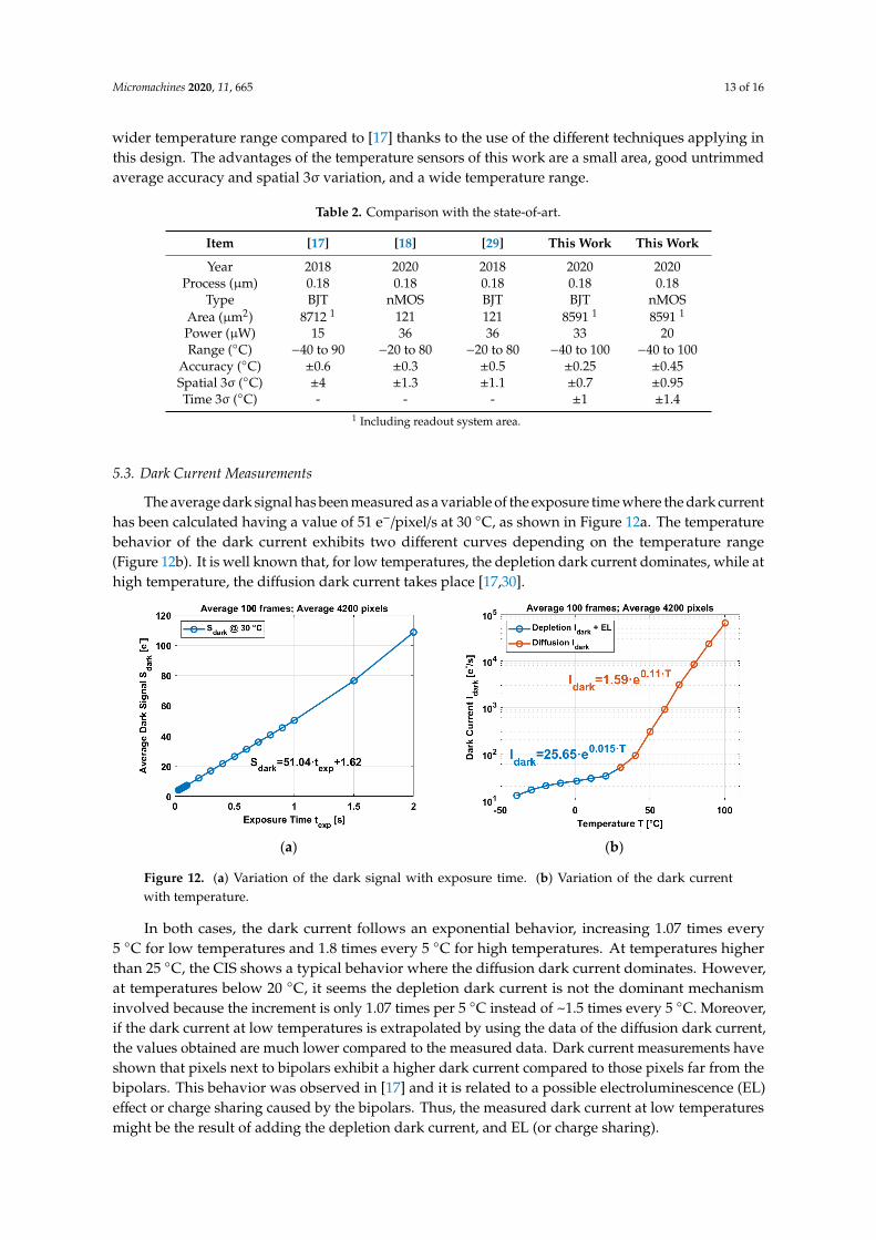
Table 2. Comparison with the state-of-art.
Item [17] [18] [29] This Work This Work
Year 2018 2020 2018 2020 2020Process (µm) 0.18 0.18 0.18 0.18 0.18
Type BJT nMOS BJT BJT nMOSArea (µm2) 8712 1 121 121 8591 1 8591 1
Power (µW) 15 36 36 33 20Range (C) −40 to 90 −20 to 80 −20 to 80 −40 to 100 −40 to 100
Accuracy (C) ±0.6 ±0.3 ±0.5 ±0.25 ±0.45Spatial 3σ (C) ±4 ±1.3 ±1.1 ±0.7 ±0.95Time 3σ (C) - - - ±1 ±1.4
1 Including readout system area.
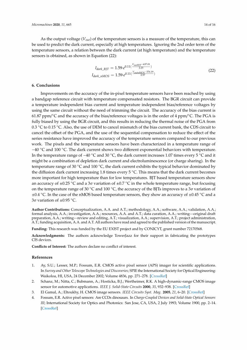
5.3. Dark Current Measurements
The average dark signal has been measured as a variable of the exposure time where the dark currenthas been calculated having a value of 51 e−/pixel/s at 30 C, as shown in Figure 12a. The temperaturebehavior of the dark current exhibits two different curves depending on the temperature range(Figure 12b). It is well known that, for low temperatures, the depletion dark current dominates, while athigh temperature, the diffusion dark current takes place [17,30].
Micromachines 2020, 11, x FOR PEER REVIEW 13 of 16
Table 2. Comparison with the state-of-art.
Item [17] [18] [29] This Work This Work Year 2018 2020 2018 2020 2020
Process (μm) 0.18 0.18 0.18 0.18 0.18 Type BJT nMOS BJT BJT nMOS
Area (μm2) 87121 121 121 8591 1 8591 1
Power (μW) 15 36 36 33 20 Range (°C) −40 to 90 −20 to 80 −20 to 80 −40 to 100 −40 to 100
Accuracy (°C) ±0.6 ±0.3 ±0.5 ±0.25 ±0.45 Spatial 3σ (°C) ±4 ±1.3 ±1.1 ±0.7 ±0.95 Time 3σ (°C) - - - ±1 ±1.4
1 Including readout system area.
5.3. Dark Current Measurements
The average dark signal has been measured as a variable of the exposure time where the dark current has been calculated having a value of 51 e−/pixel/s at 30 °C, as shown in Figure 12a. The temperature behavior of the dark current exhibits two different curves depending on the temperature range (Figure 12b). It is well known that, for low temperatures, the depletion dark current dominates, while at high temperature, the diffusion dark current takes place [17,30].
(a) (b)
Figure 12. (a) Variation of the dark signal with exposure time. (b) Variation of the dark current with temperature.
In both cases, the dark current follows an exponential behavior, increasing 1.07 times every 5 °C for low temperatures and 1.8 times every 5 °C for high temperatures. At temperatures higher than 25 °C, the CIS shows a typical behavior where the diffusion dark current dominates. However, at temperatures below 20 °C, it seems the depletion dark current is not the dominant mechanism involved because the increment is only 1.07 times per 5 °C instead of ~1.5 times every 5 °C. Moreover, if the dark current at low temperatures is extrapolated by using the data of the diffusion dark current, the values obtained are much lower compared to the measured data. Dark current measurements have shown that pixels next to bipolars exhibit a higher dark current compared to those pixels far from the bipolars. This behavior was observed in [17] and it is related to a possible electroluminescence (EL) effect or charge sharing caused by the bipolars. Thus, the measured dark current at low temperatures might be the result of adding the depletion dark current, and EL (or charge sharing).
As the output voltage ( ) of the temperature sensors is a measure of the temperature, this can be used to predict the dark current, especially at high temperatures. Ignoring the 2nd order term of the temperature sensors, a relation between the dark current (at high temperature) and the temperature sensors is obtained, as shown in Equation (22):
Figure 12. (a) Variation of the dark signal with exposure time. (b) Variation of the dark currentwith temperature.
In both cases, the dark current follows an exponential behavior, increasing 1.07 times every5 C for low temperatures and 1.8 times every 5 C for high temperatures. At temperatures higherthan 25 C, the CIS shows a typical behavior where the diffusion dark current dominates. However,at temperatures below 20 C, it seems the depletion dark current is not the dominant mechanisminvolved because the increment is only 1.07 times per 5 C instead of ~1.5 times every 5 C. Moreover,if the dark current at low temperatures is extrapolated by using the data of the diffusion dark current,the values obtained are much lower compared to the measured data. Dark current measurements haveshown that pixels next to bipolars exhibit a higher dark current compared to those pixels far from thebipolars. This behavior was observed in [17] and it is related to a possible electroluminescence (EL)effect or charge sharing caused by the bipolars. Thus, the measured dark current at low temperaturesmight be the result of adding the depletion dark current, and EL (or charge sharing).
Micromachines 2020, 11, 665 14 of 16
As the output voltage (Vout) of the temperature sensors is a measure of the temperature, this canbe used to predict the dark current, especially at high temperatures. Ignoring the 2nd order term of thetemperature sensors, a relation between the dark current (at high temperature) and the temperaturesensors is obtained, as shown in Equation (22):
Idark_BJT = 1.59·e0.11(VoutBJT−637.01
2.23 )
Idark_nMOS = 1.59·e0.11(VoutnMOS−376.19
0.97 )(22)
6. Conclusions
Improvements on the accuracy of the in-pixel temperature sensors have been reached by usinga bandgap reference circuit with temperature compensated resistors. The BGR circuit can providea temperature independent bias current and temperature independent bias/reference voltages byusing the same circuit without the need of trimming the circuit. The accuracy of the bias current is61.87 ppm/C and the accuracy of the bias/reference voltages is in the order of 4 ppm/C. The PGA isfully biased by using the BGR circuit, and this results in reducing the thermal noise of the PGA from0.3 C to 0.15 C. Also, the use of DEM to cancel mismatch of the bias current bank, the CDS circuit tocancel the offset of the PGA, and the use of the sequential compensation to reduce the effect of theseries resistance have improved the accuracy of the temperature sensors compared to our previouswork. The pixels and the temperature sensors have been characterized in a temperature range of−40 C and 100 C. The dark current shows two different exponential behaviors with temperature.In the temperature range of −40 C and 30 C, the dark current increases 1.07 times every 5 C and itmight be a combination of depletion dark current and electroluminescence (or charge sharing). In thetemperature range of 30 C and 100 C, the dark current exhibits the typical behavior dominated bythe diffusion dark current increasing 1.8 times every 5 C. This means that the dark current becomesmore important for high temperature than for low temperatures. BJT based temperature sensors showan accuracy of ±0.25 C and a 3σ variation of ±0.7 C in the whole temperature range, but focusingon the temperature range of 30 C and 100 C, the accuracy of the BJTs improves to a 3σ variation of±0.4 C. In the case of the nMOS based temperature sensors, they show an accuracy of ±0.45 C and a3σ variation of ±0.95 C.
Author Contributions: Conceptualization, A.A. and A.T.; methodology, A.A.; software, A.A.; validation, A.A.;formal analysis, A.A.; investigation, A.A.; resources, A.A. and A.T.; data curation, A.A.; writing—original draftpreparation, A.A.; writing—review and editing, A.T.; visualization, A.A.; supervision, A.T.; project administration,A.T.; funding acquisition, A.A. and A.T. All authors have read and agreed to the published version of the manuscript.
Funding: This research was funded by the EU EXIST project and by CONICYT, grant number 72170568.
Acknowledgments: The authors acknowledge TowerJazz for their support in fabricating the prototypesCIS devices.
Conflicts of Interest: The authors declare no conflict of interest.
References
1. Ay, S.U.; Lesser, M.P.; Fossum, E.R. CMOS active pixel sensor (APS) imager for scientific applications.In Survey and Other Telescope Technologies and Discoveries; SPIE the International Society for Optical Engineering:Waikoloa, HI, USA, 24 December 2002; Volume 4836, pp. 271–278. [CrossRef]
2. Schanz, M.; Nitta, C.; Bubmann, A.; Hosticka, B.J.; Wertheimer, R.K. A high-dynamic-range CMOS imagesensor for automotive applications. IEEE J. Solid-State Circuits 2000, 35, 932–938. [CrossRef]
3. El Gamal, A.; Eltoukhy, H. CMOS image sensors. IEEE Circuits Syst. Mag. 2005, 21, 6–20. [CrossRef]4. Fossum, E.R. Active pixel sensors: Are CCDs dinosaurs. In Charge-Coupled Devices and Solid-State Optical Sensors
III; International Society for Optics and Photonics: San Jose, CA, USA, 2 July 1993; Volume 1900, pp. 2–14.[CrossRef]
Micromachines 2020, 11, 665 15 of 16
5. Fossum, E.R. CMOS image sensors: Electronic camera on a chip. IEEE Trans. Electron. Devices 1997,44, 1689–1698. [CrossRef]
6. Ackland, B.; Dickinson, A. Camera-on-a-chip. In Proceedings of the ISSCC Digest of Technical Papers,San Francisco, CA, USA, 10 February 1996; pp. 22–25. [CrossRef]
7. Wuu, S.-G.; Chien, H.-C.; Yaung, D.-N.; Tseng, C.-H.; Wang, C.S.; Chang, C.-K.; Hsaio, Y.-K. A highperformance active pixel sensor with 0.18 µm CMOS color imager technology. In Proceedings of the IEDMDigest of Technical Papers, Washington, DC, USA, 2–5 December 2001; pp. 555–558. [CrossRef]
8. Law, M.; Bermark, A.; Luong, H.C. A sub-µW embedded temperature sensor for RFID food monitoringapplication. IEEE J. Solid-State Circuits 2010, 45, 1246–1255. [CrossRef]
9. Lin, Y.; Sylvester, D.; Blaauw, D. An ultra low power 1 V, 220 nW temperature sensor for passive wirelessapplications. In Proceedings of the IEEE Custom Custom Integrated Circuits Conference, San Jose, CA, USA,21–24 September 2008; pp. 507–510. [CrossRef]
10. Vaz, A.; Ubarretxena, A.; Zalbide, I.; Pardo, D.; Solar, H.; Garcia-Alonso, A.; Berenguer, R. Full Passive UHFTag With a Temperature Sensor Suitable for Human Body Temperature Monitoring. IEEE Trans. Circuits Syst.II Express Briefs 2010, 57, 95–99. [CrossRef]
11. Kwon, H.I.; Kang, I.M.; Park, B.-G.; Lee, J.D.; Park, S.S. The analysis of dark signals in the CMOS APS imagersfrom the characterization of test structures. IEEE Trans. Electron. Devices 2004, 51, 178–184. [CrossRef]
12. Wang, X. Noise in Sub-Micron CMOS Image Sensors. Ph.D. Thesis, Delft University of Technology, Delft,The Netherlands, 3 November 2008; pp. 46–68.
13. Baranov, P.S.; Litvin, V.T.; Belous, D.A.; Mantsvetov, A.A. Dark Current of the Solid-State Imagers at HighTemperature. In Proceedings of the IEEE Conference of Russian Young Researchers in Electrical andElectronic Engineering (EIConRus), St Petersburg, Russia, 1–3 February 2017; pp. 635–638. [CrossRef]
14. Widenhorn, R.; Blouke, M.M.; Weber, A.; Rest, A.; Bodegom, E. Temperature dependence of dark currentin a CCD. In Sensors and Camera Systems for Scientific, Industrial, and Digital Photography Applications III;International Society for Optics and Photonics: San Jose, CA, USA, 24 April 2002; Volume 4669, pp. 193–201.[CrossRef]
15. Han, S.-W.; Yoon, E. Low dark current CMOS image sensor pixel with photodiode structure enclosed byp-well. Electron. Lett. 2006, 42, 1145–1146. [CrossRef]
16. Wang, X.; Snoeij, M.F.; Rao, P.R.; Mierop, A.; Theuwissen, A.J. A CMOS image sensor with a buried-channelsource follower. In Proceedings of the ISSCC Digest of Technical Papers, San Francisco, CA, USA, 3–7 February2008; pp. 62–63. [CrossRef]
17. Abarca, A.; Xie, S.; Markenhof, J.; Theuwissen, A. Integration of 555 temperature sensors into a 64 × 192CMOS image sensor. Sens. Actuators A Phys. 2018, 282, 243–250. [CrossRef]
18. Xie, S.; Abarca Prouza, A.; Theuwissen, A. A CMOS-Imager-Pixel-Based Temperature Sensor for DarkCurrent Compensation. IEEE Trans. Circuits Syst. II Express Briefs 2020, 67, 255–259. [CrossRef]
19. Pertijs, M.A.P.; Makinwa, K.A.A.; Huijsing, J.H. A CMOS smart temperature sensor with a 3σ inaccuracy of±0.1 C from −55 C to 125 C. IEEE J. Solid-State Circuits 2005, 40, 2805–2815. [CrossRef]
20. Coath, R.; Crooks, J.; Godbeer, A.; Wilson, M.; Turchetta, R. Advanced pixel architectures for scientificimage sensor. In Proceedings of the Topical Workshop on Electronics for Particle Physics, Paris, France,21–25 September 2009; pp. 57–61.
21. Fossum, E.R.; Hondongwa, D.B. A review of the pinned photodiode for CCD and CMOS image sensors.IEEE J. Electron. Dev. Soc. 2014, 2, 33–43. [CrossRef]
22. Neamen, D.A. Semiconductor Physics and Devices: Basic Principles, 3rd ed.; McGraw-Hill: New York, NY, USA,2003; pp. 268–318.
23. Pertijs, M.A.P.; Huijsing, J.H. Precision Temperature Sensors in CMOS Technology, 1st ed.; Springer: Dordrecht,The Netherlands, 2006; pp. 11–46. [CrossRef]
24. Audy, J.M.; Gilbert, B. Multiple Sequential Temperature Sensing Method and Apparatus. U.S. Patent 5,195,827,4 March 1993.
25. Xie, S.; Theuwissen, A. Suppression of spatial noise and temporal noise in a CMOS image sensor. IEEE Sens. J.2020, 20, 162–170. [CrossRef]
26. Malcovati, P.; Maloberti, F.; Fiocchi, C.; Pruzzi, M. Curvature-compensated BiCMOS bandgap with 1-Vsupply voltage. IEEE J. Solid-State Circuits 2001, 36, 1076–1081. [CrossRef]

Micromachines 2020, 11, 665 16 of 16
27. Guan, X.; Wang, X.; Wang, A.; Zhao, B. A 3 V 110 µW 3.1 ppm/C curvature-compensated CMOS bandgapreference. Analog Integr. Circuit Signal Process. 2010, 62, 113–119. [CrossRef]
28. Tsividis, Y. Accurate analyzes of temperature effects in IC-VBE characteristics with application to bandgapreference sources. IEEE J. Solid-State Circuits 1980, 15, 1076–1084. [CrossRef]
29. Xie, S.; Theuwissen, A. Compensation for Process and Temperature Dependency in a CMOS Image Sensor.Sensors 2019, 19, 870. [CrossRef] [PubMed]
30. Yasutomi, K.; Sadanaga, Y.; Takasawa, T.; Itoh, S.; Kawahito, S. Dark Current Characterization of CMOSGlobal Shutter Pixels Using Pinned Storage Diodes. In Proceedings of the International Image SensorWorkshop, Hokaido, Japan, 8–11 June 2011.
© 2020 by the authors. Licensee MDPI, Basel, Switzerland. This article is an open accessarticle distributed under the terms and conditions of the Creative Commons Attribution(CC BY) license (http://creativecommons.org/licenses/by/4.0/).