P-Channel QFET MOSFET Description · ©2000 Fairchild Semiconductor Corporation FQP4P40 Rev. C0 3...
9
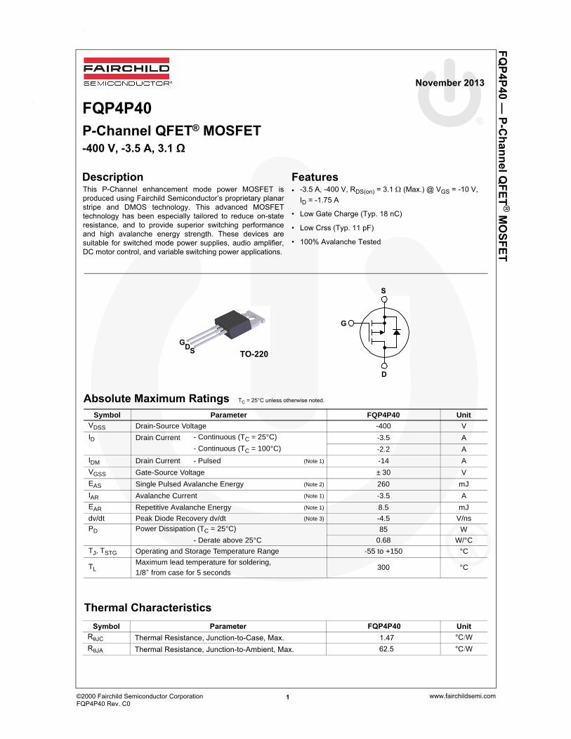
November 2013 Thermal Characteristics FQP4P40 P-Channel QFET ® MOSFET -400 V, -3.5 A, 3.1 Ω Description ©2000 Fairchild Semiconductor Corporation FQP4P40 Rev. C0 www.fairchildsemi.com 1 FQP4P40 — P-Channel QFET ® MOSFET This P-Channel enhancement mode power MOSFET is produced using Fairchild Semiconductor’s proprietary planar stripe and DMOS technology. This advanced MOSFET technology has been especially tailored to reduce on-state resistance, and to provide superior switching performance and high avalanche energy strength. These devices are suitable for switched mode power supplies, audio amplifier, DC motor control, and variable switching power applications. Features • -3.5 A, -400 V, R DS(on) = 3.1 Ω (Max.) @ V GS = -10 V, I D = -1.75 A • Low Gate Charge (Typ. 18 nC) • Low Crss (Typ. 11 pF) • 100% Avalanche Tested Absolute Maximum Ratings T C = 25°C unless otherwise noted. FQP4P40 + θ Thermal Resistance, Junction-to-Case, Max. 1.47 6? + θ Thermal Resistance, Junction-to-Ambient, Max. -'& 6? TO-220 G D S G S D Symbol Parameter FQP4P40 Unit V DSS Drain-Source Voltage -400 V I D Drain Current -3.5 A - Continuous (T C = 25°C) - Continuous (T C = 100°C) -2.2 A I DM Drain Current - Pulsed (Note 1) -14 A V GSS Gate-Source Voltage ± 30 V E AS Single Pulsed Avalanche Energy (Note 2) 260 mJ I AR Avalanche Current (Note 1) -3.5 A E AR Repetitive Avalanche Energy (Note 1) 8.5 mJ dv/dt Peak Diode Recovery dv/dt (Note 3) -4.5 V/ns P D Power Dissipation (T C = 25°C) 85 W - Derate above 25°C 0.68 W/°C T J , T STG Operating and Storage Temperature Range -55 to +150 °C T L Maximum lead temperature for soldering, 1/8" from case for 5 seconds 300 °C
Transcript of P-Channel QFET MOSFET Description · ©2000 Fairchild Semiconductor Corporation FQP4P40 Rev. C0 3...
November 2013
Thermal Characteristics
FQP4P40P-Channel QFET® MOSFET-400 V, -3.5 A, 3.1 Ω
Description
©2000 Fairchild Semiconductor Corporation FQP4P40 Rev. C0
www.fairchildsemi.com1
FQP4P40 —
P-Channel Q
FET® M
OSFET
This P-Channel enhancement mode power MOSFET is produced using Fairchild Semiconductor’s proprietary planar stripe and DMOS technology. This advanced MOSFET technology has been especially tailored to reduce on-state resistance, and to provide superior switching performance and high avalanche energy strength. These devices are suitable for switched mode power supplies, audio amplifier, DC motor control, and variable switching power applications.
Features• -3.5 A, -400 V, RDS(on) = 3.1 Ω (Max.) @ VGS = -10 V,
ID = -1.75 A
• Low Gate Charge (Typ. 18 nC)
• Low Crss (Typ. 11 pF)
• 100% Avalanche Tested
Absolute Maximum Ratings TC = 25°C unless otherwise noted.
FQP4P40
+θ Thermal Resistance, Junction-to-Case, Max. 1.47 6?
+θ Thermal Resistance, Junction-to-Ambient, Max. -' & 6?
TO-220
GDS
G
S
D
Symbol Parameter FQP4P40 Unit
VDSS Drain-Source Voltage -400 V
ID Drain Current -3.5 A- Continuous (TC = 25°C)
- Continuous (TC = 100°C) -2.2 A
IDM Drain Current - Pulsed (Note 1) -14 A
VGSS Gate-Source Voltage ± 30 V
EAS Single Pulsed Avalanche Energy (Note 2) 260 mJ
IAR Avalanche Current (Note 1) -3.5 A
EAR Repetitive Avalanche Energy (Note 1) 8.5 mJ
dv/dt Peak Diode Recovery dv/dt (Note 3) -4.5 V/ns
PD Power Dissipation (TC = 25°C) 85 W
- Derate above 25°C 0.68 W/°C
TJ, TSTG Operating and Storage Temperature Range -55 to +150 °C
TLMaximum lead temperature for soldering, 1/8" from case for 5 seconds
300 °C
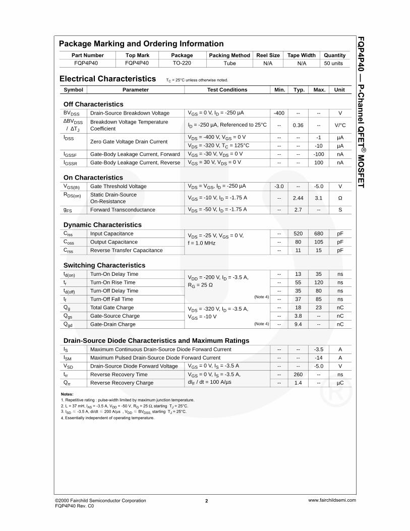
Package Marking and Ordering Information
©2000 Fairchild Semiconductor Corporation FQP4P40 Rev. C0
www.fairchildsemi.com2
FQP4P40 —
P-Channel Q
FET® M
OSFET
Electrical Characteristics TC = 25°C unless otherwise noted.
1. Repetitive rating : pulse-width limited by maximum junction temperature.2. L = 37 mH, IAS = -3.5 A, VDD = -50 V, RG = 25 Ω, starting TJ = 25°C.3. ISD ≤ -3.5 A, di/dt ≤ 200 A/µs , VDD ≤ BVDSS, starting TJ = 25°C.4. Essentially independent of operating temperature.
Notes:
Part Number Top Mark Package Reel Size Tape Width QuantityFQP4P40FQP4P40 TO-220 N/A N/A 50 units
Packing MethodTube
( N ote 4)
( Note 4)
Symbol Parameter Test Conditions Min. Typ. Max. Unit
Off CharacteristicsBVDSS Drain-Source Breakdown Voltage VGS = 0 V, ID = -250 µA -400 -- -- V
∆BVDSS
/ ∆TJ
Breakdown Voltage Temperature Coefficient
ID = -250 µA, Referenced to 25°C -- 0.36 -- V/°C
IDSSZero Gate Voltage Drain Current
VDS = -400 V, VGS = 0 V -- -- -1 µA
VDS = -320 V, TC = 125°C -- -- -10 µA
IGSSF Gate-Body Leakage Current, Forward VGS = -30 V, VDS = 0 V -- -- -100 nA
IGSSR Gate-Body Leakage Current, Reverse VGS = 30 V, VDS = 0 V -- -- 100 nA
On Characteristics VGS(th) Gate Threshold Voltage VDS = VGS, ID = -250 µA -3.0 -- -5.0 V
RDS(on) Static Drain-Source On-Resistance
VGS = -10 V, ID = -1.75 A -- 2.44 3.1 Ω
gFS Forward Transconductance VDS = -50 V, ID = -1.75 A -- 2.7 -- S
Dynamic CharacteristicsCiss Input Capacitance VDS = -25 V, VGS = 0 V,
f = 1.0 MHz
-- 520 680 pF
Coss Output Capacitance -- 80 105 pF
Crss Reverse Transfer Capacitance -- 11 15 pF
Switching Characteristics td(on) Turn-On Delay Time
VDD = -200 V, ID = -3.5 A,
RG = 25 Ω
-- 13 35 ns
tr Turn-On Rise Time -- 55 120 ns
td(off) Turn-Off Delay Time -- 35 80 ns
tf Turn-Off Fall Time -- 37 85 ns
Qg Total Gate Charge VDS = -320 V, ID = -3.5 A,
VGS = -10 V
-- 18 23 nC
Qgs Gate-Source Charge -- 3.8 -- nC
Qgd Gate-Drain Charge -- 9.4 -- nC
Drain-Source Diode Characteristics and Maximum RatingsIS Maximum Continuous Drain-Source Diode Forward Current -- -- -3.5 A
ISM Maximum Pulsed Drain-Source Diode Forward Current -- -- -14 A
VSD Drain-Source Diode Forward Voltage VGS = 0 V, IS = -3.5 A -- -- -5.0 V
trr Reverse Recovery Time VGS = 0 V, IS = -3.5 A,
dIF / dt = 100 A/µs
-- 260 -- ns
Qrr Reverse Recovery Charge -- 1.4 -- µC
©2000 Fairchild Semiconductor Corporation FQP4P40 Rev. C0
www.fairchildsemi.com3
FQP4P40 —
P-Channel Q
FET® M
OSFET
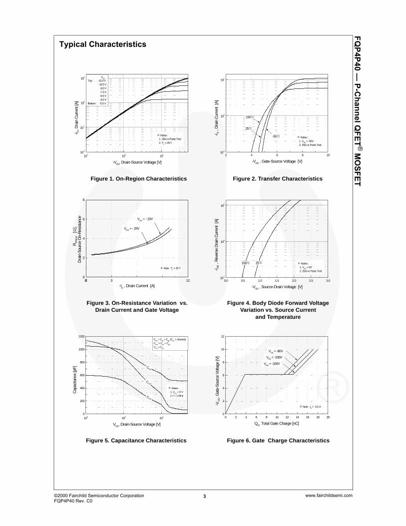
Typical Characteristics
0 2 4 6 8 10 21 41 16 81 200
2
4
6
8
10
12
VDS
= -200V
VDS
= -80V
VDS
= -320V
※ Note : ID = -3.5 A
-VG
S, G
ate-
Sou
rce
Vol
tage
[V]
QG, Total Gate Charge [nC]
10-1 0
101
0
200
400
600
800
1000
1200C
iss = C
gs + C
gd (C
ds = shorted)
Coss
= Cds
+ Cgd
Crss
= Cgd
※ Notes : 1. V
GS = 0 V
2. f = 1 MHzCrss
Coss
Ciss
Cap
acita
nce
[pF]
10
VDS
, Drain-Source Voltage [V]
0.0 0.5 1.0 1.5 2.0 2.5 3.010
-1
100
101
150 ※ Notes : 1. V
GS = 0V
2. 250μs Pulse Test
25
-ID
R ,
Rev
erse
Dra
in C
urre
nt [
A]
-VSD
, Source-Drain Voltage [V]
00 30 120
2
4
6
8
※ Note : TJ = 25
VGS
= - 20V
VGS
= - 10V
RD
S(o
n) [
Ω],
Dra
in-S
ourc
e O
n-R
esis
tanc
e
-ID , Drain Current [A]
2 6 84 1010
-1
100
101
150
25
-55 ※ Notes : 1. V
DS = -50V
2. 250μs Pulse Test
-ID ,
Dra
in C
urre
nt [
A]
-VGS
, Gate-Source Voltage [V]10
-110
010
110
-2
10-1
100
101 V
GS
Top : -15.0 V -10.0 V -8.0 V -7.0 V -6.5 V -6.0 V
Bottom : -5.5 V
※ Notes : 1. 250μs Pulse Test 2. T
C = 25
-ID, D
rain
Cur
rent
[A]
-VDS
, Drain-Source Voltage [V]
Figure 5. Capacitance Characteristics Figure 6. Gate Charge Characteristics
Figure 3. On-Resistance Variation vs.Drain Current and Gate Voltage
Figure 4. Body Diode Forward Voltage Variation vs. Source Current
and Temperature
Figure 2. Transfer CharacteristicsFigure 1. On-Region Characteristics
©2000 Fairchild Semiconductor Corporation FQP4P40 Rev. C0
www.fairchildsemi.com4
FQP4P40 —
P-Channel Q
FET® M
OSFET
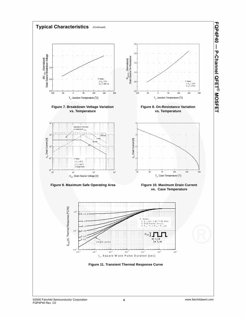
Typical Characteristics (Continued)
1 0-5
1 0-4
1 0-3
1 0-2
1 0-1
1 00
1 01
1 0-2
1 0-1
1 00
※ N o te s : 1 . Z θ J C
( t ) = 1 4 7.4 /W M a x . 2 . D u ty F a c to r , D = t
1/ t
2
3 . TJ M
- TC
= PD M
* Z θ J C( t )
s in g le p u ls e
D = 0 .5
0 .0 2
0 .2
0 .0 5
0 .1
0 .0 1
25 50 75 100 125 1500
1
2
3
4
-ID, D
rain
Cur
rent
[A]
TC, Case Temperature []
100
101
102
103
10-2
10-1
100
101
102
DC
10 ms
1 ms
100 µs
Operation in This Area is Limited by R
DS(on)
※ Notes :
1. TC = 25
oC
2. TJ = 150
oC
3. Single Pulse
-ID, D
rain
Cur
rent
[A]
-100 -50 0 50 100 150 2000.0
0.5
1.0
1.5
2.0
2.5
※ Notes : 1. V
GS = -10 V
2. ID = -1.75 A
RD
S(O
N), (
Nor
mal
ized
)D
rain
-Sou
rce
On-
Res
ista
nce
TJ, Junction Temperature [
oC]
-100 -50 0 50 100 150 2000.8
0.9
1.0
※ Notes : 1. V
GS = 0 V
2. ID = -250 μA
-BV
DSS
, (N
orm
aliz
ed)
Dra
in-S
ourc
e Br
eakd
own
Volta
ge
TJ, Junction Temperature [
oC]
-VDS
, Drain-Source Voltage [V]
Figure 9. Maximum Safe Operating Area Figure 10. Maximum Drain Currentvs. Case Temperature
Figure 7. Breakdown Voltage Variationvs. Temperature
Figure 8. On-Resistance Variationvs. Temperature
t1, S q u a re W a v e P u ls e D u ra t io n [s e c ]
Figure 11. Transient Thermal Response Curve
t1
PDM
t2
Z JC
(t), T
herm
al R
espo
nse
[o C/W
]
©2000 Fairchild Semiconductor Corporation FQP4P40 Rev. C0
www.fairchildsemi.com5
FQP4P40 —
P-Channel Q
FET® M
OSFET
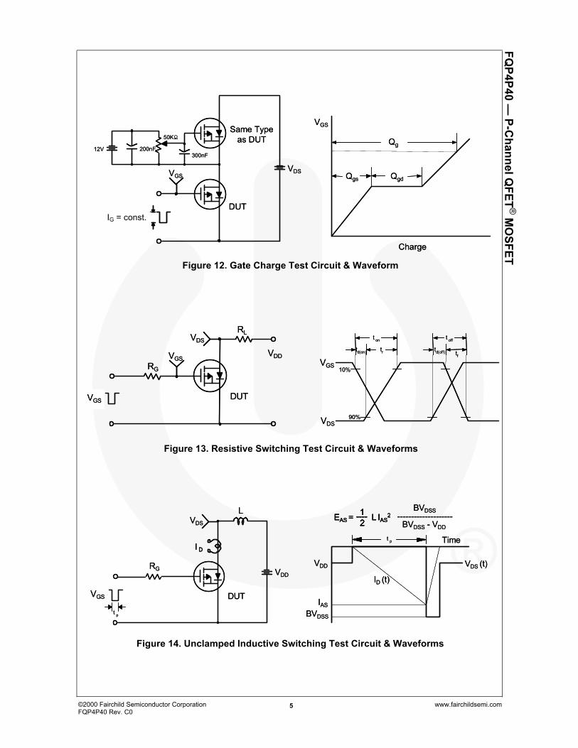
Figure 12. Gate Charge Test Circuit & Waveform
Figure 13. Resistive Switching Test Circuit & Waveforms
Figure 14. Unclamped Inductive Switching Test Circuit & Waveforms
VVDSDS
VVGSGS1010%%
90%90%
ttd(d(onon)) ttrr
tt onon tt ofofff
ttd(d(ofofff)) ttffVVDDDD
VVDSDS
RRLL
DUTDUT
RRGG
VVGSGS
ChChargargee
VVGSGS
QQgg
QQgsgs QQgdgdVVGSGS
DUDUTT
VVDSDS
300300nFnF
50K50KΩΩ
200n200nFF12V12V
SamSamee T Tyypepeas as DUDUTT
EEEAS AS AS ----=== 21212121------------ LLL ASASASIII
BVBVDSDSSS222 ----------------------------------------
BVBVDSDSSS - V- VDDDD
VVDDDD
VVDSDS
BVBVDSSDSS
t t pp
VVDDDD
IIASAS
VVDS DS (t)(t)
IID D (t(t))
TiTimmee
DUDUTT
RRGG
LLL
III DDD
t t pp
IG = const.
VVGSGS
VVGSGS
©2000 Fairchild Semiconductor Corporation FQP4P40 Rev. C0
www.fairchildsemi.com6
FQP4P40 —
P-Channel Q
FET® M
OSFET
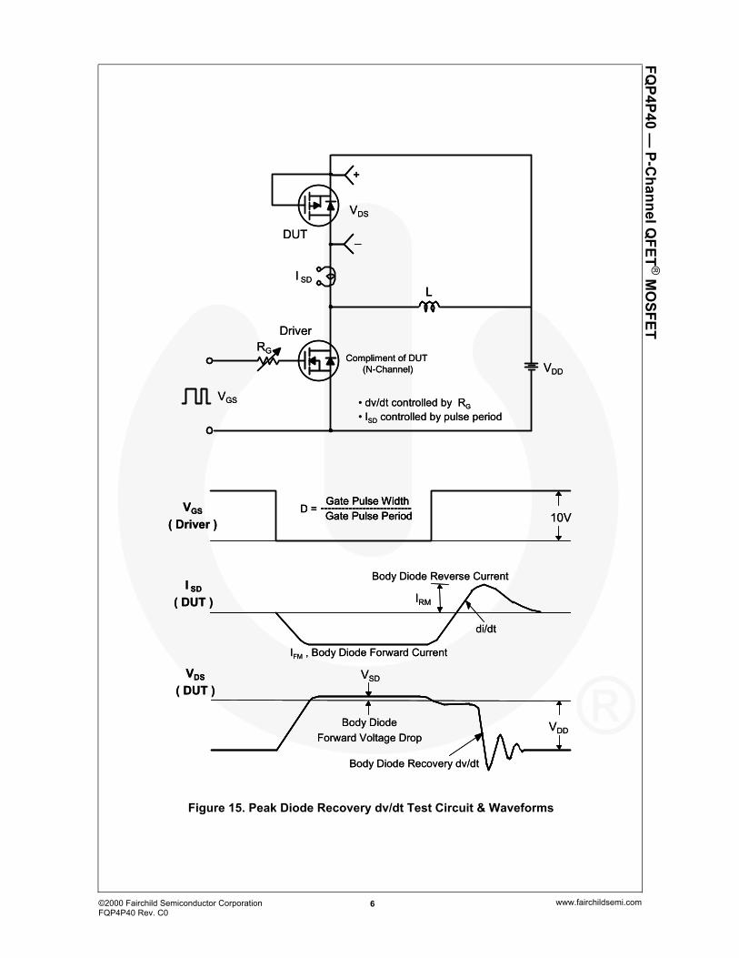
Figure 15. Peak Diode Recovery dv/dt Test Circuit & Waveforms
••
DUTDUT
VVDSDS
++
__
DrivDrivererRRGG
ComCompplliimmentent ofof DUTDUT (N-(N-CChannelhannel))
VVGSGS •• ddvv//dtdt ccoontntrroolllleed d bbyy RRGG
IISDSD ccononttrrolollleded byby pupullsse e peperriiodod
VVDDDD
LLLII SDSD
1010VVVVGSGS
( ( DrivDriver er ))
II SDSD
( ( DUT DUT ))
VVDSDS
( ( DUT DUT ))
VVDDDDBoBodydy DDiiooddee
ForForwward ard VVololttagage e DrDropop
IIFMFM ,, BoBodydy DDiiodode e FFororwwaarrd d CCuurrrrenentt
VVSDSD
BoBodydy DDiiodode e RReevveerrssee CCuurrrrenentt
IIRMRM
BoBodydy DiDiodode e RReecovcoveerryy dvdv/d/dtt
didi//dtdt
D D D === ---------GateGateGate--------------------------- PPPulululsss------------------------e e e WWWiiiddd---------------ttthhh---GaGaGate te te PuPuPulllssseee PePePerrriiiododod
©2000 Fairchild Semiconductor Corporation FQP4P40 Rev. C0
www.fairchildsemi.com7
FQP4P40 —
P-Channel Q
FET® M
OSFET
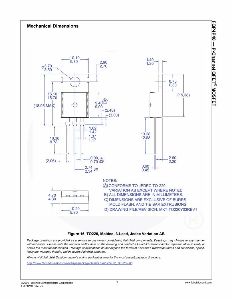
Mechanical Dimensions
Figure 16. TO220, Molded, 3-Lead, Jedec Variation ABPackage drawings are provided as a service to customers considering Fairchild components. Drawings may change in any manner without notice. Please note the revision and/or date on the drawing and contact a Fairchild Semiconductor representative to verify or obtain the most recent revision. Package specifications do not expand the terms of Fairchild’s worldwide terms and conditions, specif-ically the warranty therein, which covers Fairchild products.
Always visit Fairchild Semiconductor’s online packaging area for the most recent package drawings:
http://www.fairchildsemi.com/package/packageDetails.html?id=PN_TO220-003
©2000 Fairchild Semiconductor Corporation FQP4P40 Rev. C0
www.fairchildsemi.com8
TRADEMARKSThe following includes registered and unregistered trademarks and service marks, owned by Fairchild Semiconductor and/or its global subsidiaries, and is not intended to be an exhaustive list of all such trademarks.
*Trademarks of System General Corporation, used under license by Fairchild Semiconductor.
DISCLAIMERFAIRCHILD SEMICONDUCTOR RESERVES THE RIGHT TO MAKE CHANGES WITHOUT FURTHER NOTICE TO ANY PRODUCTS HEREIN TO IMPROVE RELIABILITY, FUNCTION, OR DESIGN. FAIRCHILD DOES NOT ASSUME ANY LIABILITY ARISING OUT OF THE APPLICATION OR USE OF ANY PRODUCT OR CIRCUIT DESCRIBED HEREIN; NEITHER DOES IT CONVEY ANY LICENSE UNDER ITS PATENT RIGHTS, NOR THE RIGHTS OF OTHERS. THESE SPECIFICATIONS DO NOT EXPAND THE TERMS OF FAIRCHILD’S WORLDWIDE TERMS AND CONDITIONS, SPECIFICALLY THE WARRANTY THEREIN, WHICH COVERS THESE PRODUCTS.
LIFE SUPPORT POLICYFAIRCHILD’S PRODUCTS ARE NOT AUTHORIZED FOR USE AS CRITICAL COMPONENTS IN LIFE SUPPORT DEVICES OR SYSTEMS WITHOUT THE EXPRESS WRITTEN APPROVAL OF FAIRCHILD SEMICONDUCTOR CORPORATION.
As used here in:1. Life support devices or systems are devices or systems which, (a) are
intended for surgical implant into the body or (b) support or sustain life, and (c) whose failure to perform when properly used in accordance with instructions for use provided in the labeling, can be reasonably expected to result in a significant injury of the user.
2. A critical component in any component of a life support, device, orsystem whose failure to perform can be reasonably expected to cause the failure of the life support device or system, or to affect its safety oreffectiveness.
PRODUCT STATUS DEFINITIONSDefinition of Terms
AccuPower™AX-CAP®*BitSiC™Build it Now™CorePLUS™CorePOWER™CROSSVOLT™CTL™Current Transfer Logic™DEUXPEED®
Dual Cool™EcoSPARK®
EfficentMax™ESBC™
Fairchild®
Fairchild Semiconductor®
FACT Quiet Series™FACT®
FAST®
FastvCore™FETBench™FPS™
F-PFS™FRFET®
Global Power ResourceSM
GreenBridge™Green FPS™Green FPS™ e-Series™Gmax™GTO™IntelliMAX™ISOPLANAR™Marking Small Speakers Sound Louder and Better™MegaBuck™MICROCOUPLER™MicroFET™MicroPak™MicroPak2™MillerDrive™MotionMax™mWSaver®
OptoHiT™OPTOLOGIC®
OPTOPLANAR®
PowerTrench®
PowerXS™Programmable Active Droop™QFET®
QS™Quiet Series™RapidConfigure™
Saving our world, 1mW/W/kW at a time™SignalWise™SmartMax™SMART START™Solutions for Your Success™SPM®
STEALTH™SuperFET®
SuperSOT™-3SuperSOT™-6SuperSOT™-8SupreMOS®
SyncFET™
Sync-Lock™®*
TinyBoost®
TinyBuck®
TinyCalc™TinyLogic®
TINYOPTO™TinyPower™TinyPWM™TinyWire™TranSiC™TriFault Detect™TRUECURRENT®*SerDes™
UHC®
Ultra FRFET™UniFET™VCX™VisualMax™VoltagePlus™XS™
®
™
Datasheet Identification Product Status Definition
Advance Information Formative / In Design Datasheet contains the design specifications for product development. Specifications may change in any manner without notice.
Preliminary First ProductionDatasheet contains preliminary data; supplementary data will be published at a later date. Fairchild Semiconductor reserves the right to make changes at any time without notice to improve design.
No Identification Needed Full Production Datasheet contains final specifications. Fairchild Semiconductor reserves the right to make changes at any time without notice to improve the design.
Obsolete Not In Production Datasheet contains specifications on a product that is discontinued by Fairchild Semiconductor. The datasheet is for reference information only.
ANTI-COUNTERFEITING POLICYFairchild Semiconductor Corporation’s Anti-Counterfeiting Policy. Fairchild’s Anti-Counterfeiting Policy is also stated on our external website, www.Fairchildsemi.com, under Sales Support.Counterfeiting of semiconductor parts is a growing problem in the industry. All manufactures of semiconductor products are experiencing counterfeiting of their parts. Customers who inadvertently purchase counterfeit parts experience many problems such as loss of brand reputation, substandard performance, failed application, and increased cost of production and manufacturing delays. Fairchild is taking strong measures to protect ourselves and our customers from the proliferation of counterfeit parts. Fairchild strongly encourages customers to purchase Fairchild parts either directly from Fairchild or from Authorized Fairchild Distributors who are listed by country on our web page cited above. Products customers buy either from Fairchild directly or from Authorized Fairchild Distributors are genuine parts, have full traceability, meet Fairchild’s quality standards for handing and storage and provide access to Fairchild’s full range of up-to-date technical and product information. Fairchild and our Authorized Distributors will stand behind all warranties and will appropriately address and warranty issues that may arise. Fairchild will not provide any warranty coverage or other assistance for parts bought from Unauthorized Sources. Fairchild is committed to combat this global problem and encourage our customers to do their part in stopping this practice by buying direct or from authorized distributors.
Rev. I66
tm
®
FQP4P40 —
P-Channel Q
FET® M
OSFET
Mouser Electronics
Authorized Distributor
Click to View Pricing, Inventory, Delivery & Lifecycle Information: Fairchild Semiconductor:
FQP4P40