OPA2188 0.03-μV/°C Drift, Low-Noise, Rail-to-Rail Output ... · PDF file145 125 105 85...
36
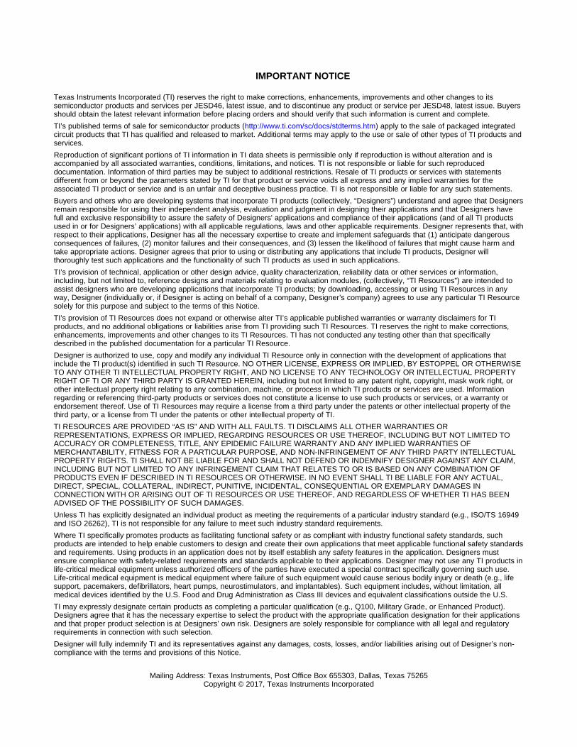
145 125 105 85 65 45 25 5 Offset Voltage ( V) m -55 -15 5 25 125 Temperature ( C) ° -35 45 65 OPA2188 Zero-Drift Architecture Precision Laser Trim Architecture 85 105 Product Folder Sample & Buy Technical Documents Tools & Software Support & Community Reference Design An IMPORTANT NOTICE at the end of this data sheet addresses availability, warranty, changes, use in safety-critical applications, intellectual property matters and other important disclaimers. PRODUCTION DATA. OPA2188 SBOS525C – AUGUST 2011 – REVISED JUNE 2016 OPA2188 0.03-μV/°C Drift, Low-Noise, Rail-to-Rail Output, 36-V, Zero-Drift Operational Amplifiers 1 1 Features 1• Low Offset Voltage: 25 μV (Maximum) • Zerø-Drift: 0.03 μV/°C • Low Noise: 8.8 nV/√Hz 0.1-Hz to 10-Hz Noise: 0.25 μV PP • Excellent DC Precision: PSRR: 142 dB CMRR: 146 dB Open-Loop Gain: 136 dB • Gain Bandwidth: 2 MHz • Quiescent Current: 475 μA (Maximum) • Wide Supply Range: ±2 V to ±18 V • Rail-to-Rail Output: Input Includes Negative Rail • RFI Filtered Inputs • MicroSIZE Packages 2 Applications • Bridge Amplifiers • Strain Gauges • Test Equipment • Transducer Applications • Temperature Measurement • Electronic Scales • Medical Instrumentation • Resistance Temperature Detectors • Precision Active Filters 3 Description The OPA2188 operational amplifier uses TI proprietary auto-zeroing techniques to provide low offset voltage (25 μV, maximum), and near zero-drift over time and temperature. This miniature, high- precision, low quiescent current amplifier offers high input impedance and rail-to-rail output swing within 15 mV of the rails. The input common-mode range includes the negative rail. Either single or dual supplies can be used in the range of 4 V to 36 V (±2 V to ±18 V). The OPA2188 device is available in MSOP-8 and SO-8 packages. The device is specified for operation from –40°C to +105°C. Device Information (1) PART NUMBER PACKAGE BODY SIZE (NOM) OPA2188 SOIC (8) 4.90 mm × 3.91 mm VSSOP (8) 3.00 mm × 3.00 mm (1) For all available packages, see the orderable addendum at the end of the data sheet. Offset Voltage vs Temperature
-
Upload
truongduong -
Category
Documents
-
view
217 -
download
4
Transcript of OPA2188 0.03-μV/°C Drift, Low-Noise, Rail-to-Rail Output ... · PDF file145 125 105 85...
145
125
105
85
65
45
25
5
Offset V
oltage (
V)
m
-55 -15 5 25 125
Temperature ( C)°
-35 45 65
OPA2188 Zero-Drift Architecture
Precision Laser Trim Architecture
85 105
Product
Folder
Sample &Buy
Technical
Documents
Tools &
Software
Support &Community
ReferenceDesign
An IMPORTANT NOTICE at the end of this data sheet addresses availability, warranty, changes, use in safety-critical applications,intellectual property matters and other important disclaimers. PRODUCTION DATA.
OPA2188SBOS525C –AUGUST 2011–REVISED JUNE 2016
OPA2188 0.03-μV/°C Drift, Low-Noise, Rail-to-Rail Output,36-V, Zero-Drift Operational Amplifiers
1
1 Features1• Low Offset Voltage: 25 μV (Maximum)• Zerø-Drift: 0.03 μV/°C• Low Noise: 8.8 nV/√Hz
0.1-Hz to 10-Hz Noise: 0.25 µVPP
• Excellent DC Precision:PSRR: 142 dBCMRR: 146 dBOpen-Loop Gain: 136 dB
• Gain Bandwidth: 2 MHz• Quiescent Current: 475 μA (Maximum)• Wide Supply Range: ±2 V to ±18 V• Rail-to-Rail Output:
Input Includes Negative Rail• RFI Filtered Inputs• MicroSIZE Packages
2 Applications• Bridge Amplifiers• Strain Gauges• Test Equipment• Transducer Applications• Temperature Measurement• Electronic Scales• Medical Instrumentation• Resistance Temperature Detectors• Precision Active Filters
3 DescriptionThe OPA2188 operational amplifier uses TIproprietary auto-zeroing techniques to provide lowoffset voltage (25 μV, maximum), and near zero-driftover time and temperature. This miniature, high-precision, low quiescent current amplifier offers highinput impedance and rail-to-rail output swing within 15mV of the rails. The input common-mode rangeincludes the negative rail. Either single or dualsupplies can be used in the range of 4 V to 36 V (±2V to ±18 V).
The OPA2188 device is available in MSOP-8 andSO-8 packages. The device is specified for operationfrom –40°C to +105°C.
Device Information(1)
PART NUMBER PACKAGE BODY SIZE (NOM)
OPA2188SOIC (8) 4.90 mm × 3.91 mmVSSOP (8) 3.00 mm × 3.00 mm
(1) For all available packages, see the orderable addendum atthe end of the data sheet.
Offset Voltage vs Temperature
2
OPA2188SBOS525C –AUGUST 2011–REVISED JUNE 2016 www.ti.com
Product Folder Links: OPA2188
Submit Documentation Feedback Copyright © 2011–2016, Texas Instruments Incorporated
Table of Contents1 Features .................................................................. 12 Applications ........................................................... 13 Description ............................................................. 14 Revision History..................................................... 25 Zero-Drift Amplifier Portfolio ................................ 36 Pin Configuration and Functions ......................... 37 Specifications......................................................... 4
7.1 Absolute Maximum Ratings ...................................... 47.2 ESD Ratings.............................................................. 47.3 Recommended Operating Conditions....................... 47.4 Thermal Information .................................................. 47.5 Electrical Characteristics: High-Voltage Operation, VS
= ±4 V to ±18 V (VS = 8 V to 36 V)............................ 57.6 Electrical Characteristics: Low-Voltage Operation, VS
= ±2 V to < ±4 V (VS = +4 V to < +8 V) ..................... 77.7 Typical Characteristics: Table of Graphs.................. 97.8 Typical Characteristics ............................................ 10
8 Detailed Description ............................................ 178.1 Overview ................................................................. 178.2 Functional Block Diagram ....................................... 17
8.3 Feature Description................................................. 188.4 Device Functional Modes........................................ 20
9 Application and Implementation ........................ 219.1 Application Information............................................ 219.2 Typical Applications ................................................ 219.3 System Examples ................................................... 22
10 Power Supply Recommendations ..................... 2311 Layout................................................................... 25
11.1 Layout Guidelines ................................................. 2511.2 Layout Example .................................................... 25
12 Device and Documentation Support ................. 2612.1 Device Support .................................................... 2612.2 Documentation Support ....................................... 2712.3 Receiving Notification of Documentation Updates 2712.4 Community Resource............................................ 2712.5 Trademarks ........................................................... 2712.6 Electrostatic Discharge Caution............................ 2712.7 Glossary ................................................................ 27
13 Mechanical, Packaging, and OrderableInformation ........................................................... 27
4 Revision HistoryNOTE: Page numbers for previous revisions may differ from page numbers in the current version.
Changes from Revision B (September 2012) to Revision C Page
• Added ESD Ratings table, Feature Description section, Device Functional Modes, Application and Implementationsection, Power Supply Recommendations section, Layout section, Device and Documentation Support section, andMechanical, Packaging, and Orderable Information section ................................................................................................. 1
• Changed Input Bias Current, IB and IOS parameters overtemperature maximum specification in ElectricalCharacteristics: High-Voltage Operation table ....................................................................................................................... 5
• Changed Noise, Input voltage noise density parameter units in Electrical Characteristics: High-Voltage Operation table... 5• Changed Power Supply, IQ parameter maximum specifications in Electrical Characteristics: High-Voltage Operation
table ....................................................................................................................................................................................... 6• Changed Input Bias Current, IB and IOS parameters overtemperature maximum specification in Electrical
Characteristics: Low-Voltage Operation table ....................................................................................................................... 7• Changed Noise, Input voltage noise density parameter units in Electrical Characteristics: Low-Voltage Operation
table ....................................................................................................................................................................................... 7• Changed Power Supply, IQ parameter maximum specifications in Electrical Characteristics: Low-Voltage Operation
table ....................................................................................................................................................................................... 8
Changes from Revision A (June 2012) to Revision B Page
• Changed second to last Applications bullet............................................................................................................................ 1
Changes from Original (August 2011) to Revision A Page
• Deleted all references to OPA188 and OPA4188 throughout document ............................................................................... 1• Updated document to current standards ................................................................................................................................ 1• Changed document status to Production Data....................................................................................................................... 1
1
2
3
4
8
7
6
5
V+
OUT B
-IN B
+IN B
OUT A
-IN A
+IN A
V-
A
B
3
OPA2188www.ti.com SBOS525C –AUGUST 2011–REVISED JUNE 2016
Product Folder Links: OPA2188
Submit Documentation FeedbackCopyright © 2011–2016, Texas Instruments Incorporated
5 Zero-Drift Amplifier Portfolio
VERSION PRODUCT OFFSET VOLTAGE (µV) OFFSET VOLTAGE DRIFT(µV/°C) BANDWIDTH (MHz)
Single
OPA188 (4 V to 36 V) 25 0.085 2
OPA333 (5 V) 10 0.05 0.35
OPA378 (5 V) 50 0.25 0.9
OPA735 (12 V) 5 0.05 1.6
Dual
OPA2188 (4 V to 36 V) 25 0.085 2
OPA2333 (5 V) 10 0.05 0.35
OPA2378 (5 V) 50 0.25 0.9
OPA2735 (12 V) 5 0.05 1.6
QuadOPA4188 (4 V to 36 V) 25 0.085 2
OPA4330 (5 V) 50 0.25 0.35
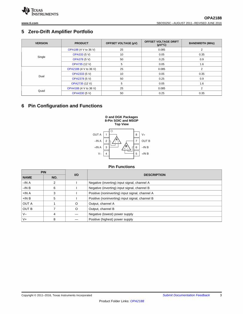
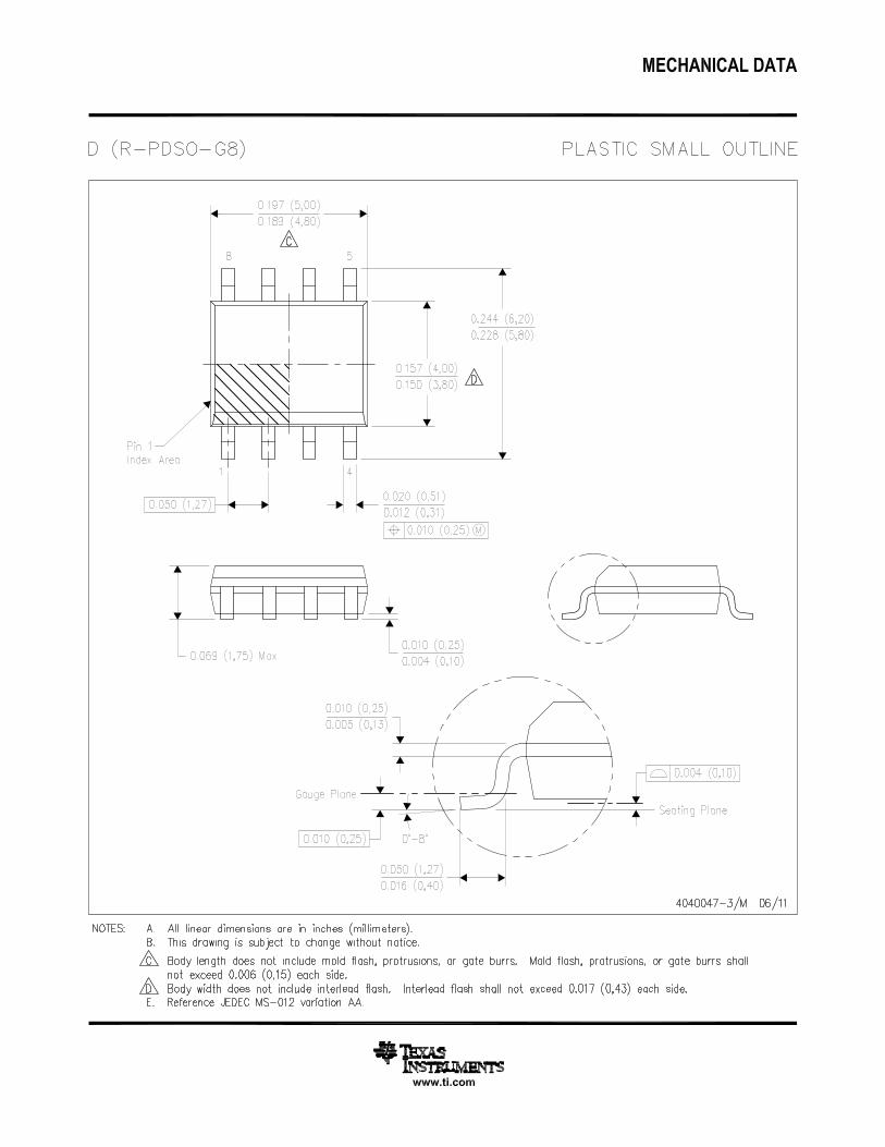
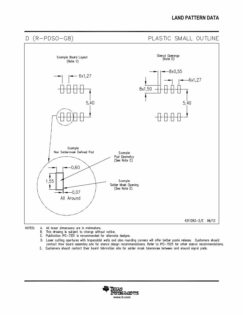
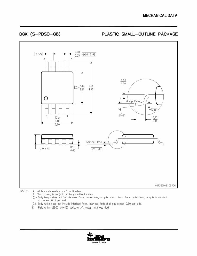
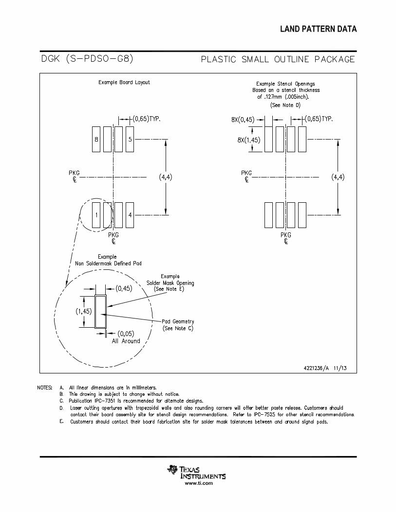
6 Pin Configuration and Functions
D and DGK Packages8-Pin SOIC and MSOP
Top View
Pin FunctionsPIN
I/O DESCRIPTIONNAME NO.–IN A 2 I Negative (inverting) input signal, channel A–IN B 6 I Negative (inverting) input signal, channel B+IN A 3 I Positive (noninverting) input signal, channel A+IN B 5 I Positive (noninverting) input signal, channel BOUT A 1 O Output, channel AOUT B 7 O Output, channel BV– 4 — Negative (lowest) power supplyV+ 8 — Positive (highest) power supply
4
OPA2188SBOS525C –AUGUST 2011–REVISED JUNE 2016 www.ti.com
Product Folder Links: OPA2188
Submit Documentation Feedback Copyright © 2011–2016, Texas Instruments Incorporated
(1) Stresses beyond those listed under Absolute Maximum Ratings may cause permanent damage to the device. These are stress ratingsonly, which do not imply functional operation of the device at these or any other conditions beyond those indicated under RecommendedOperating Conditions. Exposure to absolute-maximum-rated conditions for extended periods may affect device reliability.
(2) Input terminals are diode-clamped to the power-supply rails. Input signals that can swing more than 0.5 V beyond the supply rails shouldbe current-limited to 10 mA or less.
(3) Short-circuit to ground, one amplifier per package.
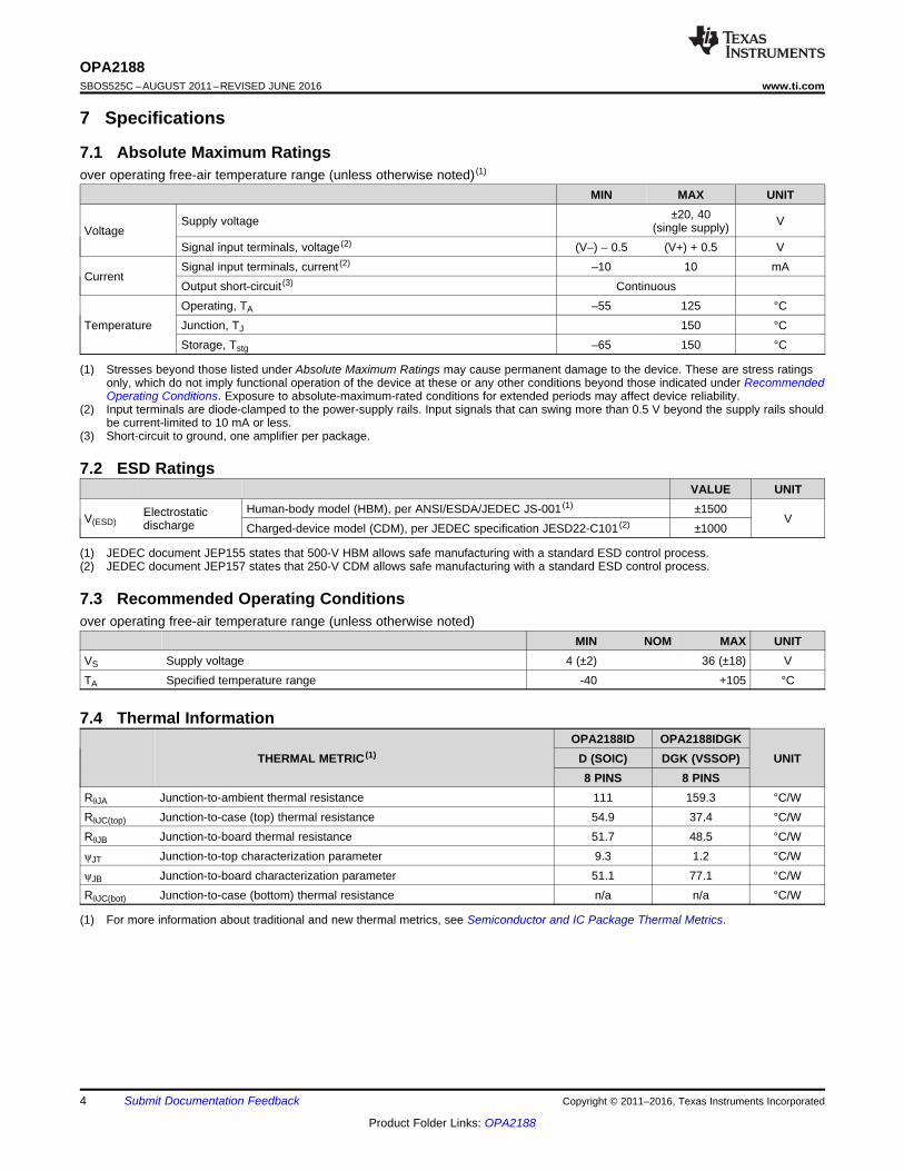
7 Specifications
7.1 Absolute Maximum Ratingsover operating free-air temperature range (unless otherwise noted) (1)
MIN MAX UNIT
VoltageSupply voltage ±20, 40
(single supply) V
Signal input terminals, voltage (2) (V–) – 0.5 (V+) + 0.5 V
CurrentSignal input terminals, current (2) –10 10 mAOutput short-circuit (3) Continuous
TemperatureOperating, TA –55 125 °CJunction, TJ 150 °CStorage, Tstg –65 150 °C
(1) JEDEC document JEP155 states that 500-V HBM allows safe manufacturing with a standard ESD control process.(2) JEDEC document JEP157 states that 250-V CDM allows safe manufacturing with a standard ESD control process.
7.2 ESD RatingsVALUE UNIT
V(ESD)Electrostaticdischarge
Human-body model (HBM), per ANSI/ESDA/JEDEC JS-001 (1) ±1500V
Charged-device model (CDM), per JEDEC specification JESD22-C101 (2) ±1000
7.3 Recommended Operating Conditionsover operating free-air temperature range (unless otherwise noted)
MIN NOM MAX UNITVS Supply voltage 4 (±2) 36 (±18) VTA Specified temperature range -40 +105 °C
(1) For more information about traditional and new thermal metrics, see Semiconductor and IC Package Thermal Metrics.
7.4 Thermal Information
THERMAL METRIC (1)OPA2188ID OPA2188IDGK
UNITD (SOIC) DGK (VSSOP)8 PINS 8 PINS
RθJA Junction-to-ambient thermal resistance 111 159.3 °C/WRθJC(top) Junction-to-case (top) thermal resistance 54.9 37.4 °C/WRθJB Junction-to-board thermal resistance 51.7 48.5 °C/WψJT Junction-to-top characterization parameter 9.3 1.2 °C/WψJB Junction-to-board characterization parameter 51.1 77.1 °C/WRθJC(bot) Junction-to-case (bottom) thermal resistance n/a n/a °C/W
5
OPA2188www.ti.com SBOS525C –AUGUST 2011–REVISED JUNE 2016
Product Folder Links: OPA2188
Submit Documentation FeedbackCopyright © 2011–2016, Texas Instruments Incorporated
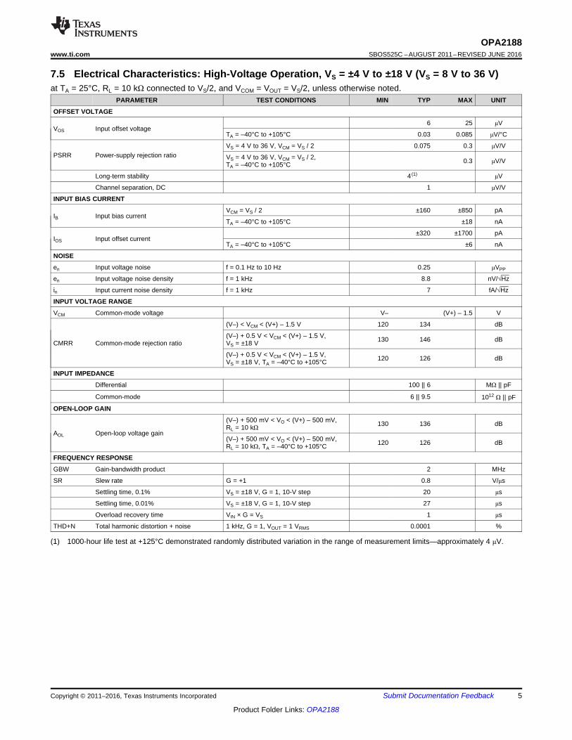
(1) 1000-hour life test at +125°C demonstrated randomly distributed variation in the range of measurement limits—approximately 4 μV.
7.5 Electrical Characteristics: High-Voltage Operation, VS = ±4 V to ±18 V (VS = 8 V to 36 V)at TA = 25°C, RL = 10 kΩ connected to VS/2, and VCOM = VOUT = VS/2, unless otherwise noted.
PARAMETER TEST CONDITIONS MIN TYP MAX UNIT
OFFSET VOLTAGE
VOS Input offset voltage6 25 μV
TA = –40°C to +105°C 0.03 0.085 μV/°C
PSRR Power-supply rejection ratioVS = 4 V to 36 V, VCM = VS / 2 0.075 0.3 μV/V
VS = 4 V to 36 V, VCM = VS / 2,TA = –40°C to +105°C 0.3 μV/V
Long-term stability 4 (1) μV
Channel separation, DC 1 μV/V
INPUT BIAS CURRENT
IB Input bias currentVCM = VS / 2 ±160 ±850 pA
TA = –40°C to +105°C ±18 nA
IOS Input offset current±320 ±1700 pA
TA = –40°C to +105°C ±6 nA
NOISE
en Input voltage noise f = 0.1 Hz to 10 Hz 0.25 μVPP
en Input voltage noise density f = 1 kHz 8.8 nV/√Hz
in Input current noise density f = 1 kHz 7 fA/√Hz
INPUT VOLTAGE RANGE
VCM Common-mode voltage V– (V+) – 1.5 V
CMRR Common-mode rejection ratio
(V–) < VCM < (V+) – 1.5 V 120 134 dB
(V–) + 0.5 V < VCM < (V+) – 1.5 V,VS = ±18 V 130 146 dB
(V–) + 0.5 V < VCM < (V+) – 1.5 V,VS = ±18 V, TA = –40°C to +105°C 120 126 dB
INPUT IMPEDANCE
Differential 100 || 6 MΩ || pF
Common-mode 6 || 9.5 1012 Ω || pF
OPEN-LOOP GAIN
AOL Open-loop voltage gain
(V–) + 500 mV < VO < (V+) – 500 mV,RL = 10 kΩ 130 136 dB
(V–) + 500 mV < VO < (V+) – 500 mV,RL = 10 kΩ, TA = –40°C to +105°C 120 126 dB
FREQUENCY RESPONSE
GBW Gain-bandwidth product 2 MHz
SR Slew rate G = +1 0.8 V/μs
Settling time, 0.1% VS = ±18 V, G = 1, 10-V step 20 μs
Settling time, 0.01% VS = ±18 V, G = 1, 10-V step 27 μs
Overload recovery time VIN × G = VS 1 μs
THD+N Total harmonic distortion + noise 1 kHz, G = 1, VOUT = 1 VRMS 0.0001 %
6
OPA2188SBOS525C –AUGUST 2011–REVISED JUNE 2016 www.ti.com
Product Folder Links: OPA2188
Submit Documentation Feedback Copyright © 2011–2016, Texas Instruments Incorporated
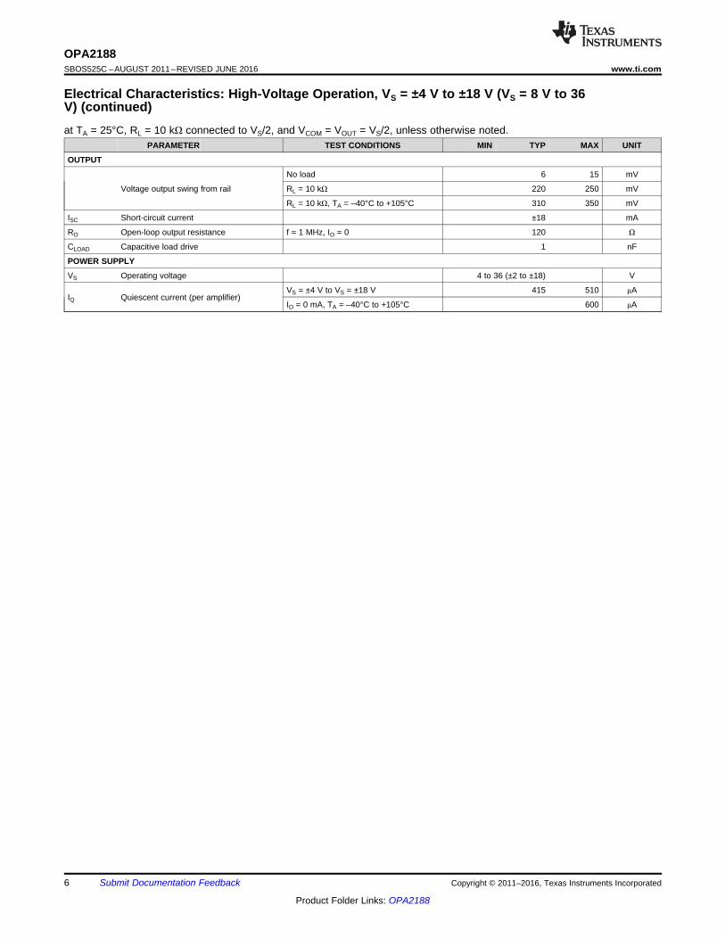
Electrical Characteristics: High-Voltage Operation, VS = ±4 V to ±18 V (VS = 8 V to 36V) (continued)at TA = 25°C, RL = 10 kΩ connected to VS/2, and VCOM = VOUT = VS/2, unless otherwise noted.
PARAMETER TEST CONDITIONS MIN TYP MAX UNIT
OUTPUT
Voltage output swing from rail
No load 6 15 mV
RL = 10 kΩ 220 250 mV
RL = 10 kΩ, TA = –40°C to +105°C 310 350 mV
ISC Short-circuit current ±18 mA
RO Open-loop output resistance f = 1 MHz, IO = 0 120 Ω
CLOAD Capacitive load drive 1 nF
POWER SUPPLY
VS Operating voltage 4 to 36 (±2 to ±18) V
IQ Quiescent current (per amplifier)VS = ±4 V to VS = ±18 V 415 510 μA
IO = 0 mA, TA = –40°C to +105°C 600 μA
7
OPA2188www.ti.com SBOS525C –AUGUST 2011–REVISED JUNE 2016
Product Folder Links: OPA2188
Submit Documentation FeedbackCopyright © 2011–2016, Texas Instruments Incorporated
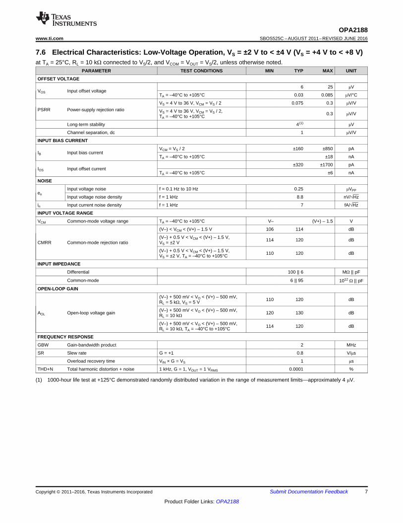
(1) 1000-hour life test at +125°C demonstrated randomly distributed variation in the range of measurement limits—approximately 4 μV.
7.6 Electrical Characteristics: Low-Voltage Operation, VS = ±2 V to < ±4 V (VS = +4 V to < +8 V)at TA = 25°C, RL = 10 kΩ connected to VS/2, and VCOM = VOUT = VS/2, unless otherwise noted.
PARAMETER TEST CONDITIONS MIN TYP MAX UNIT
OFFSET VOLTAGE
VOS Input offset voltage6 25 μV
TA = –40°C to +105°C 0.03 0.085 μV/°C
PSRR Power-supply rejection ratioVS = 4 V to 36 V, VCM = VS / 2 0.075 0.3 μV/V
VS = 4 V to 36 V, VCM = VS / 2,TA = –40°C to +105°C 0.3 μV/V
Long-term stability 4 (1) μV
Channel separation, dc 1 μV/V
INPUT BIAS CURRENT
IB Input bias currentVCM = VS / 2 ±160 ±850 pA
TA = –40°C to +105°C ±18 nA
IOS Input offset current±320 ±1700 pA
TA = –40°C to +105°C ±6 nA
NOISE
enInput voltage noise f = 0.1 Hz to 10 Hz 0.25 μVPP
Input voltage noise density f = 1 kHz 8.8 nV/√Hz
in Input current noise density f = 1 kHz 7 fA/√Hz
INPUT VOLTAGE RANGE
VCM Common-mode voltage range TA = –40°C to +105°C V– (V+) – 1.5 V
CMRR Common-mode rejection ratio
(V–) < VCM < (V+) – 1.5 V 106 114 dB
(V–) + 0.5 V < VCM < (V+) – 1.5 V,VS = ±2 V 114 120 dB
(V–) + 0.5 V < VCM < (V+) – 1.5 V,VS = ±2 V, TA = –40°C to +105°C 110 120 dB
INPUT IMPEDANCE
Differential 100 || 6 MΩ || pF
Common-mode 6 || 95 1012 Ω || pF
OPEN-LOOP GAIN
AOL Open-loop voltage gain
(V–) + 500 mV < VO < (V+) – 500 mV,RL = 5 kΩ, VS = 5 V 110 120 dB
(V–) + 500 mV < VO < (V+) – 500 mV,RL = 10 kΩ 120 130 dB
(V–) + 500 mV < VO < (V+) – 500 mV,RL = 10 kΩ, TA = –40°C to +105°C 114 120 dB
FREQUENCY RESPONSE
GBW Gain-bandwidth product 2 MHz
SR Slew rate G = +1 0.8 V/μs
Overload recovery time VIN × G = VS 1 μs
THD+N Total harmonic distortion + noise 1 kHz, G = 1, VOUT = 1 VRMS 0.0001 %
8
OPA2188SBOS525C –AUGUST 2011–REVISED JUNE 2016 www.ti.com
Product Folder Links: OPA2188
Submit Documentation Feedback Copyright © 2011–2016, Texas Instruments Incorporated
Electrical Characteristics: Low-Voltage Operation, VS = ±2 V to < ±4 V (VS = +4 V to < +8V) (continued)at TA = 25°C, RL = 10 kΩ connected to VS/2, and VCOM = VOUT = VS/2, unless otherwise noted.
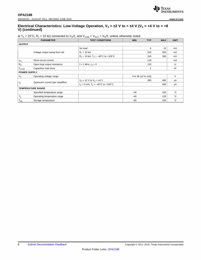
PARAMETER TEST CONDITIONS MIN TYP MAX UNIT
OUTPUT
Voltage output swing from rail
No load 6 15 mV
RL = 10 kΩ 220 250 mV
RL = 10 kΩ, TA = –40°C to +105°C 310 350 mV
ISC Short-circuit current ±18 mA
RO Open-loop output resistance f = 1 MHz, IO = 0 120 Ω
CLOAD Capacitive load drive 1 nF
POWER SUPPLY
VS Operating voltage range 4 to 36 (±2 to ±18) V
IQ Quiescent current (per amplifier)VS = ±2 V to VS = ±4 V 385 485 μA
IO = 0 mA, TA = –40°C to +105°C 590 μA
TEMPERATURE RANGE
Specified temperature range –40 105 °C
TA Operating temperature range –40 125 °C
Tstg Storage temperature –65 150 °C
9
OPA2188www.ti.com SBOS525C –AUGUST 2011–REVISED JUNE 2016
Product Folder Links: OPA2188
Submit Documentation FeedbackCopyright © 2011–2016, Texas Instruments Incorporated
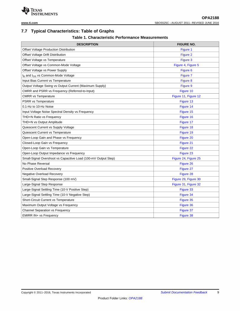
7.7 Typical Characteristics: Table of GraphsTable 1. Characteristic Performance Measurements
DESCRIPTION FIGURE NO.Offset Voltage Production Distribution Figure 1Offset Voltage Drift Distribution Figure 2Offset Voltage vs Temperature Figure 3Offset Voltage vs Common-Mode Voltage Figure 4, Figure 5Offset Voltage vs Power Supply Figure 6IB and IOS vs Common-Mode Voltage Figure 7Input Bias Current vs Temperature Figure 8Output Voltage Swing vs Output Current (Maximum Supply) Figure 9CMRR and PSRR vs Frequency (Referred-to-Input) Figure 10CMRR vs Temperature Figure 11, Figure 12PSRR vs Temperature Figure 130.1-Hz to 10-Hz Noise Figure 14Input Voltage Noise Spectral Density vs Frequency Figure 15THD+N Ratio vs Frequency Figure 16THD+N vs Output Amplitude Figure 17Quiescent Current vs Supply Voltage Figure 18Quiescent Current vs Temperature Figure 19Open-Loop Gain and Phase vs Frequency Figure 20Closed-Loop Gain vs Frequency Figure 21Open-Loop Gain vs Temperature Figure 22Open-Loop Output Impedance vs Frequency Figure 23Small-Signal Overshoot vs Capacitive Load (100-mV Output Step) Figure 24, Figure 25No Phase Reversal Figure 26Positive Overload Recovery Figure 27Negative Overload Recovery Figure 28Small-Signal Step Response (100 mV) Figure 29, Figure 30Large-Signal Step Response Figure 31, Figure 32Large-Signal Settling Time (10-V Positive Step) Figure 33Large-Signal Settling Time (10-V Negative Step) Figure 34Short-Circuit Current vs Temperature Figure 35Maximum Output Voltage vs Frequency Figure 36Channel Separation vs Frequency Figure 37EMIRR IN+ vs Frequency Figure 38
15
10
5
0
5
10
15
-
-
-
V(
V)
mO
S
-20 -15 -10 -5 0 20
V (V)CM
5 Typical Units Shown
V = 18 VS ±
15105
15
10
5
0
5
10
15
-
-
-
V(
V)
mO
S
0 2 4 6 8 20
V (V)SUPPLY
5 Typical Units Shown
V = 2 V to 18 VSUPPLY ± ±
161210 1814
15
10
5
0
5
10
15
-
-
-
V(
V)
mO
S
-55 -35 -15 5 25 125
Temperature ( C)°
45 1058565
5 Typical Units Shown
V = 18 VS ±
15
10
5
0
5
10
15
-
-
-
V(
V)
mO
S
-2.5 -2 -1.5 -1 -0.5 0 2.5
V (V)CM
5 Typical Units Shown
V = 2 VS ±
21.510.5
0.0
1
0.0
2
0.0
3
0.0
4
0.0
5
0.0
6
0.0
7
0.0
8
0.0
9
Offset Voltage Drift ( V/ C)m °
Perc
enta
ge o
f A
mplif
iers
(%
)
40
35
30
25
20
15
10
5
0
0.1
Distribution Taken From 78 Amplifiers
-20
-18
-16
-14
-10
-8
-6
-4
-2 0 2 4 6 8
10
12
14
16
18
20
Offset Voltage ( V)m
Perc
enta
ge o
f A
mplif
iers
(%
)
20
18
16
14
12
10
8
6
4
2
0
Distribution Taken From 1400 Amplifiers-12
10
OPA2188SBOS525C –AUGUST 2011–REVISED JUNE 2016 www.ti.com
Product Folder Links: OPA2188
Submit Documentation Feedback Copyright © 2011–2016, Texas Instruments Incorporated
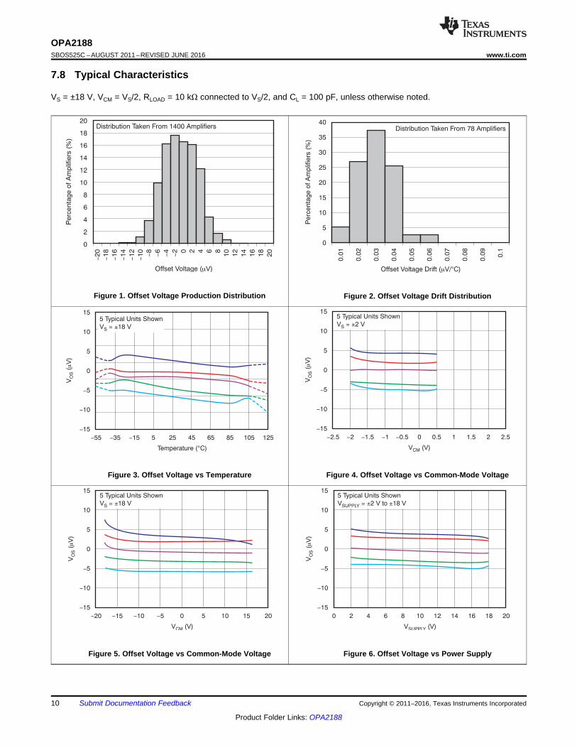
7.8 Typical Characteristics
VS = ±18 V, VCM = VS/2, RLOAD = 10 kΩ connected to VS/2, and CL = 100 pF, unless otherwise noted.
Figure 1. Offset Voltage Production Distribution Figure 2. Offset Voltage Drift Distribution
Figure 3. Offset Voltage vs Temperature Figure 4. Offset Voltage vs Common-Mode Voltage
Figure 5. Offset Voltage vs Common-Mode Voltage Figure 6. Offset Voltage vs Power Supply
40
35
30
25
20
15
10
5
0
Co
mm
on
-Mo
de
Re
jectio
n R
atio
(V
/V)
m
-55 -35 -15 5 25 125
Temperature ( C)°
45 1058565
(V ) < V < (V+) 1.5 V- CM -
(V ) + 0.5 V < V < (V+) 1.5 V- -CM
V = 2 V±SUPPLY
8
7
6
5
4
3
2
1
0
Co
mm
on
-Mo
de
Re
jectio
n R
atio
(V
/V)
m
-55 -35 -15 5 25 125
Temperature ( C)°
45 1058565
(V ) < V < (V+) 1.5 V- CM -
(V ) + 0.5 V < V < (V+) 1.5 V- -CM
V = 18 V±SUPPLY
20
Ou
tpu
t V
olta
ge
(V
)
0 2 4 6 8 24
Output Current (mA)
10 12 18
17
16
15
14
-14
-15
-16
-17
-20
1614
- °40 C
+85 C°
+125 C°
2220
19
18
-19
-18
160
140
120
100
80
60
40
20
0
Co
mm
on
-Mo
de
Re
jectio
n R
atio
(d
B),
Po
we
r-S
up
ply
Re
jectio
n R
atio
(d
B)
1 10 100 1k 10k 1M
Frequency (Hz)
100k
+PSRR
-PSRR
CMRR
500
400
300
200
100
0
100
200
300
-
-
-
Iand I
(pA
)B
OS
-20 -10 -5 0 5 20
V (V)CM
10-15
+IB
-IB
IOS
15
4000
3000
2000
1000
0
1000
2000
-
-
Input B
ias C
urr
ent (p
A)
-55 -35 -15 5 25 125
Temperature ( C)°
45 1058565
IB+
IB-
IOS
11
OPA2188www.ti.com SBOS525C –AUGUST 2011–REVISED JUNE 2016
Product Folder Links: OPA2188
Submit Documentation FeedbackCopyright © 2011–2016, Texas Instruments Incorporated
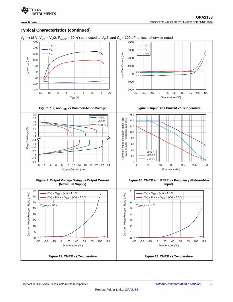
Typical Characteristics (continued)VS = ±18 V, VCM = VS/2, RLOAD = 10 kΩ connected to VS/2, and CL = 100 pF, unless otherwise noted.
Figure 7. IB and IOS vs Common-Mode Voltage Figure 8. Input Bias Current vs Temperature
Figure 9. Output Voltage Swing vs Output Current(Maximum Supply)
Figure 10. CMRR and PSRR vs Frequency (Referred-to-Input)
Figure 11. CMRR vs Temperature Figure 12. CMRR vs Temperature
0.5
0.48
0.46
0.44
0.42
0.4
0.38
0.36
0.34
0.32
0.3
I(m
A)
Q
0 4 8 12 16 36
Supply Voltage (V)
32282420
Specified Supply-Voltage Range
0.1
0.01
0.001
0.0001
0.00001
Tota
l H
arm
onic
Dis
tort
ion +
Nois
e (
%)
0.01 0.1 1 10 20
Output Amplitude (V )RMS
-60
80
100
120
140
-
-
-
-
Tota
l Harm
onic
Dis
tortio
n +
Nois
e (d
B)
BW = 80 kHz
G = +1, R = 10 kWL
G = 1, R = 10 k- WL
0.01
0.001
0.0001
0.00001
Tota
l H
arm
on
ic D
isto
rtio
n +
No
ise
(%
)
10 100 1k 10k 20k
Frequency (Hz)
Tota
l Ha
rmo
nic
Dis
tortio
n +
No
ise
(dB
)
V = 1 V
BW = 80 kHzOUT RMS
G = +1, R = 10 kWL
G = 1, R = 10 k- WL
-80
-100
-120
-140
100
10
1
Vo
lta
ge
No
ise
De
nsity (
nV
/)
ÖH
z
0.1 10 100 1k 10k 100k
Frequency (Hz)
1
1
0.8
0.6
0.4
0.2
0
0.2
0.4
0.6
0.8
1
-
-
-
-
-
Pow
er-
Supply
Reje
ction R
atio (
V/V
)m
-55 -35 -15 5 25 125
Temperature ( C)°
45 1058565
5 Typical Units Shown
V = 2 V to 18 VSUPPLY ± ±
50 n
V/d
iv
Time (1 s/div)
Peak-to-Peak Noise = 250 nV
12
OPA2188SBOS525C –AUGUST 2011–REVISED JUNE 2016 www.ti.com
Product Folder Links: OPA2188
Submit Documentation Feedback Copyright © 2011–2016, Texas Instruments Incorporated
Typical Characteristics (continued)VS = ±18 V, VCM = VS/2, RLOAD = 10 kΩ connected to VS/2, and CL = 100 pF, unless otherwise noted.
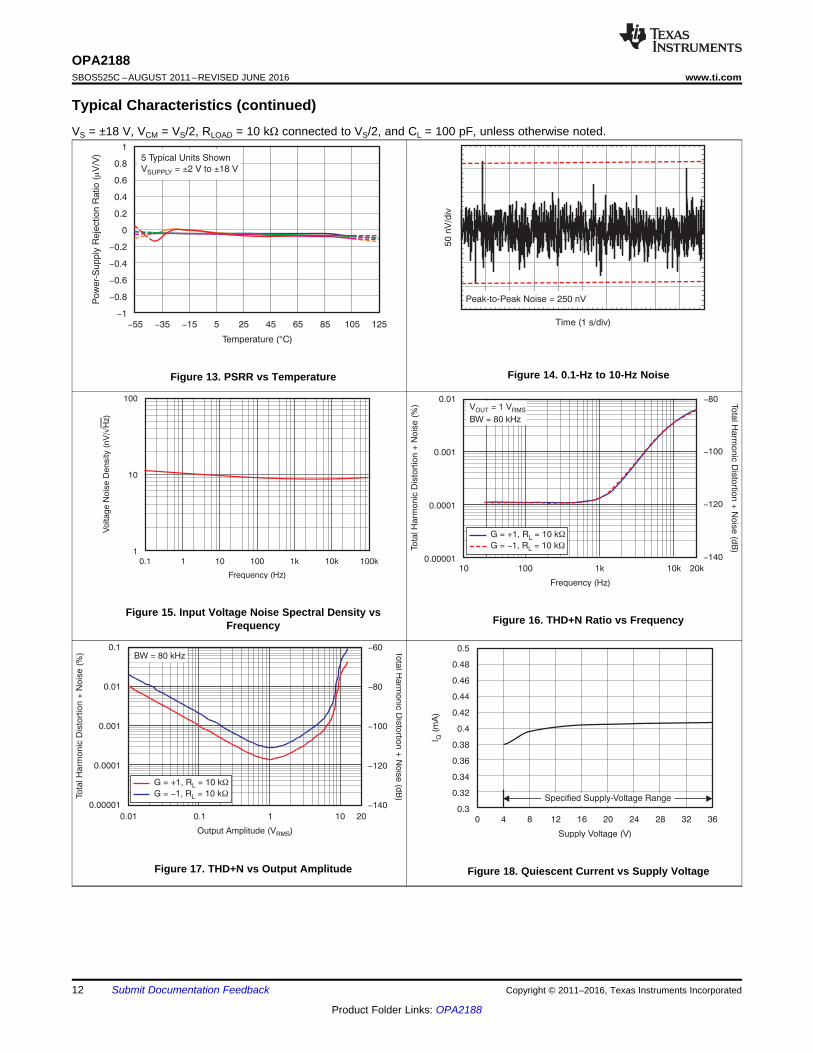
Figure 13. PSRR vs Temperature Figure 14. 0.1-Hz to 10-Hz Noise
Figure 15. Input Voltage Noise Spectral Density vsFrequency Figure 16. THD+N Ratio vs Frequency
Figure 17. THD+N vs Output Amplitude Figure 18. Quiescent Current vs Supply Voltage
10k
1k
100
10
1
1m
Z(
)W
O
1 10 100 1k 10k 10M
Frequency (Hz)
100k 1M
40
35
30
25
20
15
10
5
0
Ove
rsh
oo
t (%
)
0 100 200 300 400 500 600 700 800 900 1000
Capacitive Load (pF)
+18 V
-18 V
ROUT
CL
Device
RL
G = +1
R = 0 WOUT
R = 25 WOUT
R = 50 WOUT
R = kWL 10
25
20
15
10
5
0
5
10
15
20
-
-
-
-
Gain
(dB
)
10k 10M
Frequency (Hz)
1M100k
G = 10
G = +1
G = 1-
3
2.5
2
1.5
1
0.5
0
A(
V/V
)m
OL
-55 -35 -15 5 25 125
Temperature ( C)°
45 1058565
V = 4 V, R = 10 kWSUPPLY L
V = 36 V, R = 10 kWSUPPLY L
0.5
0.48
0.46
0.44
0.42
0.4
0.38
0.36
0.34
0.32
0.3
I(m
A)
Q
-55 -35 -15 5 25 125
Temperature ( C)°
45 1058565
V = 18 V±S
V = 2 V±S
1 10 100 1k 10k 100k 1M 10M 100M−20
0
20
40
60
80
100
120
140
0
45
90
135
180
Frequency (Hz)
Gai
n (d
B)
Pha
se (
°)
GainPhase
G001
13
OPA2188www.ti.com SBOS525C –AUGUST 2011–REVISED JUNE 2016
Product Folder Links: OPA2188
Submit Documentation FeedbackCopyright © 2011–2016, Texas Instruments Incorporated
Typical Characteristics (continued)VS = ±18 V, VCM = VS/2, RLOAD = 10 kΩ connected to VS/2, and CL = 100 pF, unless otherwise noted.
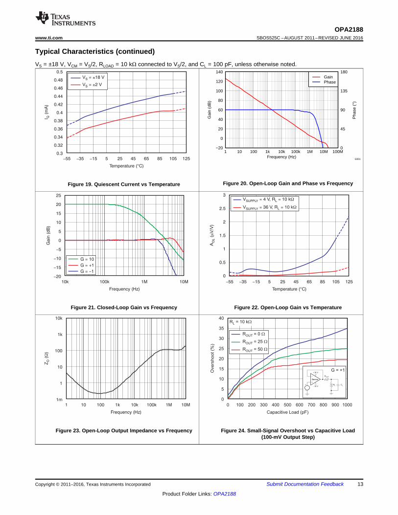
Figure 19. Quiescent Current vs Temperature Figure 20. Open-Loop Gain and Phase vs Frequency
Figure 21. Closed-Loop Gain vs Frequency Figure 22. Open-Loop Gain vs Temperature
Figure 23. Open-Loop Output Impedance vs Frequency Figure 24. Small-Signal Overshoot vs Capacitive Load(100-mV Output Step)
20 m
V/d
iv
Time (1 s/div)m
+18 V
-18 V CLRL
Device
G = +1
R = 10 k
C = 10 pF
WL
L
Time (20 s/div)m
20
mV
/div
+18 V
-18 V
R 2 kWF =R 2 kWI =
CL
Device
G = 1-
R = 10 k
C = 10 pF
WL
L
Time (5 s/div)m
5 V
/div
VIN
VOUT
2 kW
20 kW
VIN
VOUTDevice
G = 10-
+18 V
-18 V
Time (5 s/div)m
5 V
/div
VIN
VOUT
2 kW
20 kW
VIN
VOUTDevice
G = 10-
+18 V
-18 V
40
35
30
25
20
15
10
5
0
Overs
hoot (%
)
0 100 200 300 400 500 600 700 800 900 1000
Capacitive Load (pF)
Device
R =I 10 kW
ROUT
CL
RF = 10 kW
+18 V
-18 V
G = 1-
R = 0 WOUT
R = 25 WOUT
R = 50 WOUT
R = 10 kWL
Time (100 s/div)m
5 V
/div
+18 V
-18 V
37 VPP
Sine Wave
( 18.5 V)±
Device
VIN
VOUT
14
OPA2188SBOS525C –AUGUST 2011–REVISED JUNE 2016 www.ti.com
Product Folder Links: OPA2188
Submit Documentation Feedback Copyright © 2011–2016, Texas Instruments Incorporated
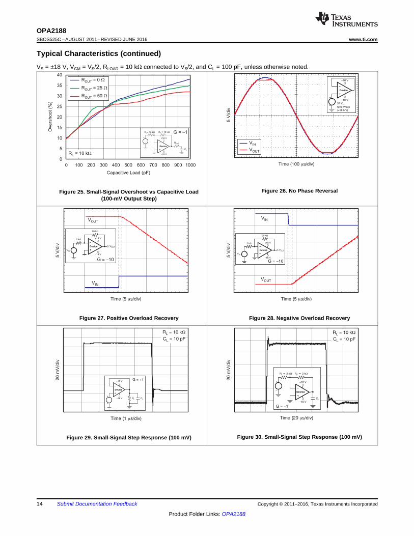
Typical Characteristics (continued)VS = ±18 V, VCM = VS/2, RLOAD = 10 kΩ connected to VS/2, and CL = 100 pF, unless otherwise noted.
Figure 25. Small-Signal Overshoot vs Capacitive Load(100-mV Output Step)
Figure 26. No Phase Reversal
Figure 27. Positive Overload Recovery Figure 28. Negative Overload Recovery
Figure 29. Small-Signal Step Response (100 mV) Figure 30. Small-Signal Step Response (100 mV)
30
20
10
0
10
20
30
-
-
-
I(m
A)
SC
-55 -35 -15 5 25 125
Temperature ( C)°
45 1058565
I , SourceSC
I , SinkSC
15
12.5
10
7.5
5
2.5
0
Ou
tpu
t V
olta
ge
(V
)P
P
1k 100k 1M 10M
Frequency (Hz)
V = 15 V±S
V = 5 V±S
V = 2.25 V±S
Maximum output voltage without
slew-rate induced distortion.
10k
10
8
6
4
2
0
2
4
6
8
10
-
-
-
-
-
DF
rom
Fin
al V
alu
e (
mV
)
0 60
Time ( s)m
2010 504030
12-Bit Settling
( 1/2 LSB = 0.024%)± ±
G = 1-10
8
6
4
2
0
2
4
6
8
10
-
-
-
-
-
DF
rom
Fin
al V
alu
e (
mV
)
0 60
Time ( s)m
2010 504030
12-Bit Settling
( 1/2 LSB = 0.024%)± ±
G = 1-
5 V
/div
Time (50 s/div)m
G = +1
R = 10 k
C = 10 pFL W
L
Time (50 s/div)m
5 V
/div
G = 1
R = 10 k
C = 10 pF
-
WL
L
15
OPA2188www.ti.com SBOS525C –AUGUST 2011–REVISED JUNE 2016
Product Folder Links: OPA2188
Submit Documentation FeedbackCopyright © 2011–2016, Texas Instruments Incorporated
Typical Characteristics (continued)VS = ±18 V, VCM = VS/2, RLOAD = 10 kΩ connected to VS/2, and CL = 100 pF, unless otherwise noted.
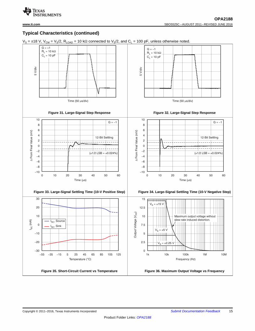
Figure 31. Large-Signal Step Response Figure 32. Large-Signal Step Response
Figure 33. Large-Signal Settling Time (10-V Positive Step) Figure 34. Large-Signal Settling Time (10-V Negative Step)
Figure 35. Short-Circuit Current vs Temperature Figure 36. Maximum Output Voltage vs Frequency
-60
70
80
90
100
110
120
130
140
150
-
-
-
-
-
-
-
-
-
Ch
an
ne
l S
ep
ara
tio
n (
dB
)
1 100 1k 10k 100M
Frequency (Hz)
10 100k 1M 10M
Channel A to B
Channel B to A
160
140
120
100
80
60
40
20
0
EM
IRR
IN
+ (
dB
)
10M 10G
Frequency (Hz)
100M 1G
16
OPA2188SBOS525C –AUGUST 2011–REVISED JUNE 2016 www.ti.com
Product Folder Links: OPA2188
Submit Documentation Feedback Copyright © 2011–2016, Texas Instruments Incorporated
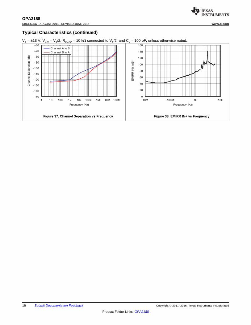
Typical Characteristics (continued)VS = ±18 V, VCM = VS/2, RLOAD = 10 kΩ connected to VS/2, and CL = 100 pF, unless otherwise noted.
Figure 37. Channel Separation vs Frequency Figure 38. EMIRR IN+ vs Frequency
GM1
+IN
-IN
CHOP1 CHOP2NotchFilter
GM_FF
GM2 GM3
C2
C1
OUT
17
OPA2188www.ti.com SBOS525C –AUGUST 2011–REVISED JUNE 2016
Product Folder Links: OPA2188
Submit Documentation FeedbackCopyright © 2011–2016, Texas Instruments Incorporated
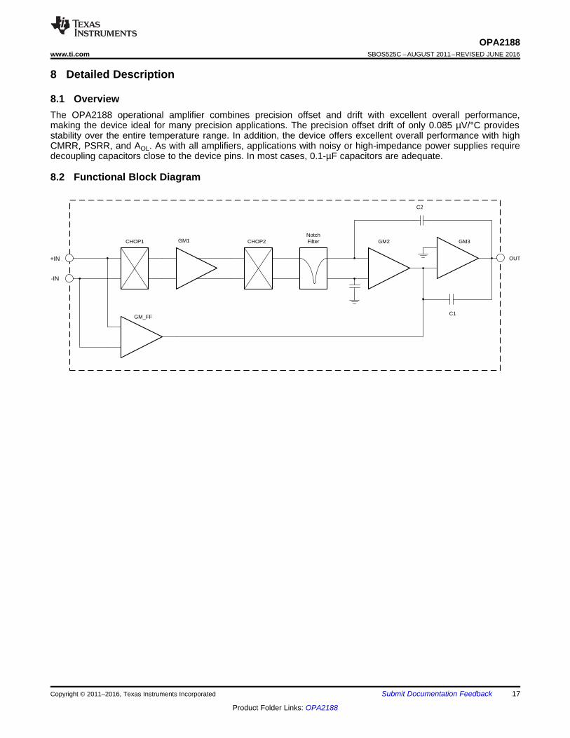
8 Detailed Description
8.1 OverviewThe OPA2188 operational amplifier combines precision offset and drift with excellent overall performance,making the device ideal for many precision applications. The precision offset drift of only 0.085 µV/°C providesstability over the entire temperature range. In addition, the device offers excellent overall performance with highCMRR, PSRR, and AOL. As with all amplifiers, applications with noisy or high-impedance power supplies requiredecoupling capacitors close to the device pins. In most cases, 0.1-µF capacitors are adequate.
8.2 Functional Block Diagram
Time (100 s/div)m
5 V
/div
+18 V
-18 V
37 VPP
Sine Wave
( 18.5 V)±
Device
VIN
VOUT
160
140
120
100
80
60
40
20
0
EM
IRR
IN
+ (
dB
)
10M 10G
Frequency (Hz)
100M 1G
18
OPA2188SBOS525C –AUGUST 2011–REVISED JUNE 2016 www.ti.com
Product Folder Links: OPA2188
Submit Documentation Feedback Copyright © 2011–2016, Texas Instruments Incorporated
8.3 Feature Description
8.3.1 Operating CharacteristicsThe OPA2188 is specified for operation from 4 V to 36 V (±2 V to ±18 V). Many of the specifications apply from–40°C to +105°C. Parameters that can exhibit significant variance with regard to operating voltage ortemperature are presented in the Typical Characteristics.
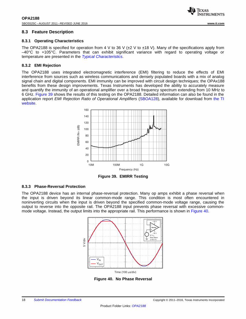
8.3.2 EMI RejectionThe OPA2188 uses integrated electromagnetic interference (EMI) filtering to reduce the effects of EMIinterference from sources such as wireless communications and densely populated boards with a mix of analogsignal chain and digital components. EMI immunity can be improved with circuit design techniques; the OPAx188benefits from these design improvements. Texas Instruments has developed the ability to accurately measureand quantify the immunity of an operational amplifier over a broad frequency spectrum extending from 10 MHz to6 GHz. Figure 39 shows the results of this testing on the OPA2188. Detailed information can also be found in theapplication report EMI Rejection Ratio of Operational Amplifiers (SBOA128), available for download from the TIwebsite.
Figure 39. EMIRR Testing
8.3.3 Phase-Reversal ProtectionThe OPA2188 device has an internal phase-reversal protection. Many op amps exhibit a phase reversal whenthe input is driven beyond its linear common-mode range. This condition is most often encountered innoninverting circuits when the input is driven beyond the specified common-mode voltage range, causing theoutput to reverse into the opposite rail. The OPA2188 input prevents phase reversal with excessive common-mode voltage. Instead, the output limits into the appropriate rail. This performance is shown in Figure 40.
Figure 40. No Phase Reversal
5 kWDevice
10 mA max
V+
VIN
VOUT
IOVERLOAD
40
35
30
25
20
15
10
5
0
Ove
rsh
oo
t (%
)
0 100 200 300 400 500 600 700 800 900 1000
Capacitive Load (pF)
+18 V
-18 V
ROUT
CL
Device
RL
G = +1
R = 0 WOUT
R = 25 WOUT
R = 50 WOUT
R = kWL 1040
35
30
25
20
15
10
5
0
Overs
hoot (%
)
0 100 200 300 400 500 600 700 800 900 1000
Capacitive Load (pF)
Device
R =I 10 kW
ROUT
CL
RF = 10 kW
+18 V
-18 V
G = 1-
R = 0 WOUT
R = 25 WOUT
R = 50 WOUT
R = 10 kWL
19
OPA2188www.ti.com SBOS525C –AUGUST 2011–REVISED JUNE 2016
Product Folder Links: OPA2188
Submit Documentation FeedbackCopyright © 2011–2016, Texas Instruments Incorporated
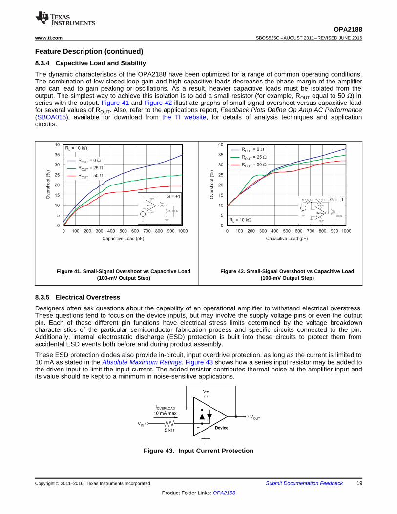
Feature Description (continued)8.3.4 Capacitive Load and StabilityThe dynamic characteristics of the OPA2188 have been optimized for a range of common operating conditions.The combination of low closed-loop gain and high capacitive loads decreases the phase margin of the amplifierand can lead to gain peaking or oscillations. As a result, heavier capacitive loads must be isolated from theoutput. The simplest way to achieve this isolation is to add a small resistor (for example, ROUT equal to 50 Ω) inseries with the output. Figure 41 and Figure 42 illustrate graphs of small-signal overshoot versus capacitive loadfor several values of ROUT. Also, refer to the applications report, Feedback Plots Define Op Amp AC Performance(SBOA015), available for download from the TI website, for details of analysis techniques and applicationcircuits.
Figure 41. Small-Signal Overshoot vs Capacitive Load(100-mV Output Step)
Figure 42. Small-Signal Overshoot vs Capacitive Load(100-mV Output Step)
8.3.5 Electrical OverstressDesigners often ask questions about the capability of an operational amplifier to withstand electrical overstress.These questions tend to focus on the device inputs, but may involve the supply voltage pins or even the outputpin. Each of these different pin functions have electrical stress limits determined by the voltage breakdowncharacteristics of the particular semiconductor fabrication process and specific circuits connected to the pin.Additionally, internal electrostatic discharge (ESD) protection is built into these circuits to protect them fromaccidental ESD events both before and during product assembly.
These ESD protection diodes also provide in-circuit, input overdrive protection, as long as the current is limited to10 mA as stated in the Absolute Maximum Ratings. Figure 43 shows how a series input resistor may be added tothe driven input to limit the input current. The added resistor contributes thermal noise at the amplifier input andits value should be kept to a minimum in noise-sensitive applications.
Figure 43. Input Current Protection
20
OPA2188SBOS525C –AUGUST 2011–REVISED JUNE 2016 www.ti.com
Product Folder Links: OPA2188
Submit Documentation Feedback Copyright © 2011–2016, Texas Instruments Incorporated
Feature Description (continued)An ESD event produces a short duration, high-voltage pulse that is transformed into a short duration, high-current pulse as it discharges through a semiconductor device. The ESD protection circuits are designed toprovide a current path around the operational amplifier core to prevent it from being damaged. The energyabsorbed by the protection circuitry is then dissipated as heat.
When the operational amplifier connects into a circuit, the ESD protection components are intended to remaininactive and not become involved in the application circuit operation. However, circumstances may arise wherean applied voltage exceeds the operating voltage range of a given pin. Should this condition occur, there is a riskthat some of the internal ESD protection circuits may be biased on, and conduct current. Any such current flowoccurs through ESD cells and rarely involves the absorption device.
If there is an uncertainty about the ability of the supply to absorb this current, external zener diodes may beadded to the supply pins. The zener voltage must be selected such that the diode does not turn on during normaloperation.
However, its zener voltage must be low enough so that the zener diode conducts if the supply pin begins to riseabove the safe operating supply voltage level.
8.4 Device Functional ModesThe OPA2188 device has a single functional mode. The device is powered on as long as the power supplyvoltage is between 4 V (±2 V) and 36 V (±18 V).
V+
ILOAD
A1
A2
Q1
Q2
+
+
+±
VIN
RLOADRS1
RS2 RS3
IRS1
IRS2 IRS3
VRS2 VRS3
VRS1 VLOAD
V+
C6
C7
R3
R5
R4
R2
470 4.7
2200 pF
330
10 k
200
1000 pF
10 k
2 k
Copyright © 2016, Texas Instruments Incorporated
21
OPA2188www.ti.com SBOS525C –AUGUST 2011–REVISED JUNE 2016
Product Folder Links: OPA2188
Submit Documentation FeedbackCopyright © 2011–2016, Texas Instruments Incorporated
9 Application and Implementation
NOTEInformation in the following applications sections is not part of the TI componentspecification, and TI does not warrant its accuracy or completeness. TI’s customers areresponsible for determining suitability of components for their purposes. Customers shouldvalidate and test their design implementation to confirm system functionality.
9.1 Application Information
9.2 Typical Applications
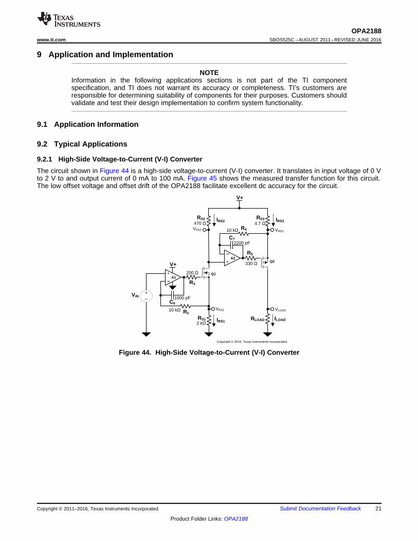
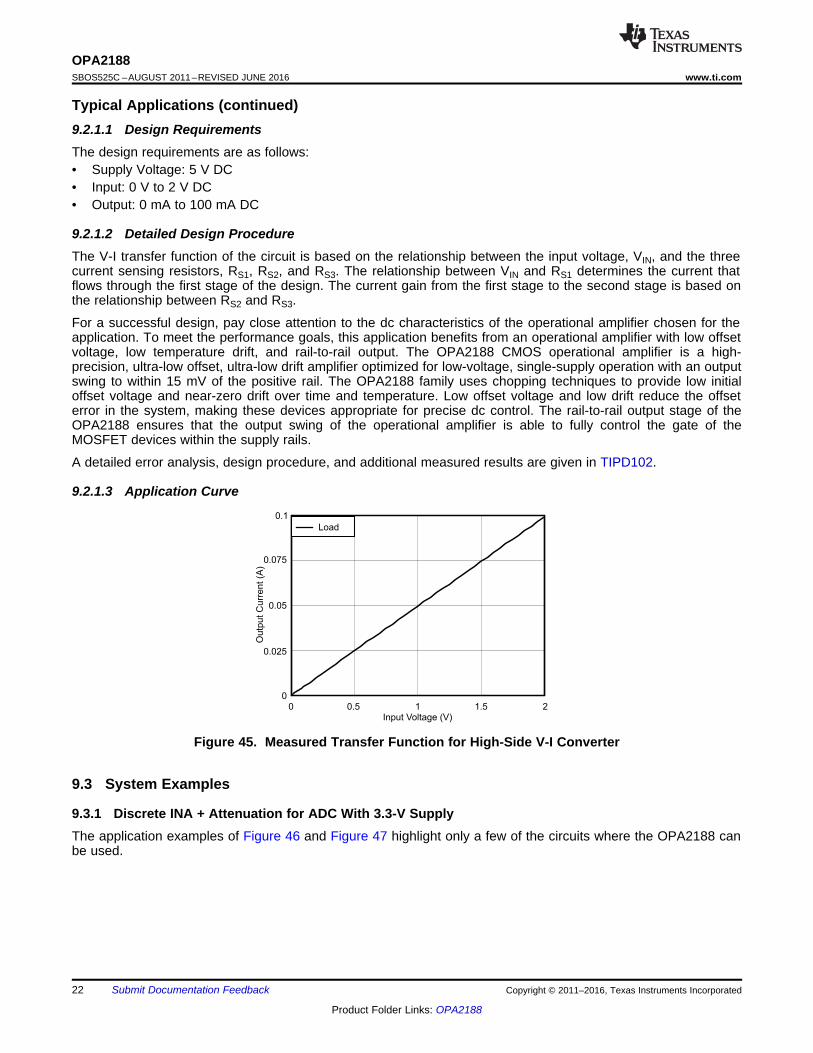
9.2.1 High-Side Voltage-to-Current (V-I) ConverterThe circuit shown in Figure 44 is a high-side voltage-to-current (V-I) converter. It translates in input voltage of 0 Vto 2 V to and output current of 0 mA to 100 mA. Figure 45 shows the measured transfer function for this circuit.The low offset voltage and offset drift of the OPA2188 facilitate excellent dc accuracy for the circuit.
Figure 44. High-Side Voltage-to-Current (V-I) Converter
Input Voltage (V)
Ou
tpu
t C
urr
en
t (A
)
0 0.5 1 1.50
0.025
0.05
0.1
Load
0.075
2
D001
22
OPA2188SBOS525C –AUGUST 2011–REVISED JUNE 2016 www.ti.com
Product Folder Links: OPA2188
Submit Documentation Feedback Copyright © 2011–2016, Texas Instruments Incorporated
Typical Applications (continued)9.2.1.1 Design RequirementsThe design requirements are as follows:• Supply Voltage: 5 V DC• Input: 0 V to 2 V DC• Output: 0 mA to 100 mA DC
9.2.1.2 Detailed Design ProcedureThe V-I transfer function of the circuit is based on the relationship between the input voltage, VIN, and the threecurrent sensing resistors, RS1, RS2, and RS3. The relationship between VIN and RS1 determines the current thatflows through the first stage of the design. The current gain from the first stage to the second stage is based onthe relationship between RS2 and RS3.
For a successful design, pay close attention to the dc characteristics of the operational amplifier chosen for theapplication. To meet the performance goals, this application benefits from an operational amplifier with low offsetvoltage, low temperature drift, and rail-to-rail output. The OPA2188 CMOS operational amplifier is a high-precision, ultra-low offset, ultra-low drift amplifier optimized for low-voltage, single-supply operation with an outputswing to within 15 mV of the positive rail. The OPA2188 family uses chopping techniques to provide low initialoffset voltage and near-zero drift over time and temperature. Low offset voltage and low drift reduce the offseterror in the system, making these devices appropriate for precise dc control. The rail-to-rail output stage of theOPA2188 ensures that the output swing of the operational amplifier is able to fully control the gate of theMOSFET devices within the supply rails.
A detailed error analysis, design procedure, and additional measured results are given in TIPD102.
9.2.1.3 Application Curve
Figure 45. Measured Transfer Function for High-Side V-I Converter
9.3 System Examples
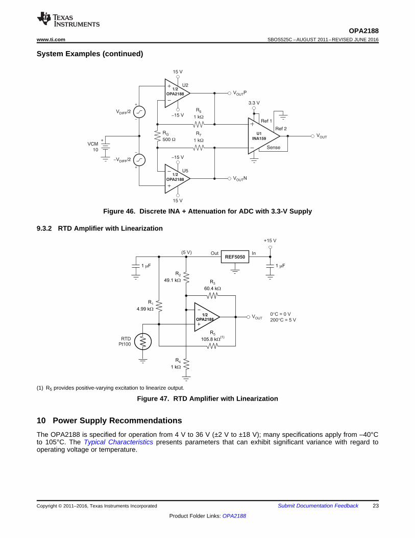
9.3.1 Discrete INA + Attenuation for ADC With 3.3-V SupplyThe application examples of Figure 46 and Figure 47 highlight only a few of the circuits where the OPA2188 canbe used.
1/2
OPA2188
RTDPt100
R
105.8 k5
W(1)
VOUT
R
60.4 k3
W
R
4.99 k1
W
R
49.1 k2
W
R
1 kW
4
1 Fm 1 Fm
REF5050
+15 V
InOut(5 V)
0 C = 0 V
200 C = 5 V
°
°
1/2
OPA2188
-15 V
15 V
U5
1/2
OPA2188
15 V
-15 V
U2
+VCM
10
-VDIFF/2
VDIFF/2 R
1 kW
5
R
1 kW
7R
500 W
G
V POUT
V NOUT
U1
INA159
3.3 V
VOUT
Ref 1
Ref 2
Sense
23
OPA2188www.ti.com SBOS525C –AUGUST 2011–REVISED JUNE 2016
Product Folder Links: OPA2188
Submit Documentation FeedbackCopyright © 2011–2016, Texas Instruments Incorporated
System Examples (continued)
Figure 46. Discrete INA + Attenuation for ADC with 3.3-V Supply
9.3.2 RTD Amplifier with Linearization
(1) R5 provides positive-varying excitation to linearize output.
Figure 47. RTD Amplifier with Linearization
10 Power Supply RecommendationsThe OPA2188 is specified for operation from 4 V to 36 V (±2 V to ±18 V); many specifications apply from –40°Cto 105°C. The Typical Characteristics presents parameters that can exhibit significant variance with regard tooperating voltage or temperature.
24
OPA2188SBOS525C –AUGUST 2011–REVISED JUNE 2016 www.ti.com
Product Folder Links: OPA2188
Submit Documentation Feedback Copyright © 2011–2016, Texas Instruments Incorporated
CAUTIONSupply voltages larger than 40 V can permanently damage the device (see theAbsolute Maximum Ratings).
TI recommends placing 0.1-μF bypass capacitors close to the power-supply pins to reduce errors coupling infrom noisy or high-impedance power supplies. For more detailed information on bypass capacitor placement,refer to the Layout Guidelines section.
GND
GND
GND
GND
InputOutput
V+
V-
OUT A
-IN A
+IN A
V-
V+
OUT B
-IN B
+IN B
+
±
+
±
Input
OutputA
B
Copyright © 2016, Texas Instruments Incorporated
Place power supply bypass capacitors close to the device
Place power supply bypass capacitors close to the device
Keep high impedance input traces short
Keep high impedance input traces short
Connect to low impedance ground plane
Connect to low impedance ground plane
25
OPA2188www.ti.com SBOS525C –AUGUST 2011–REVISED JUNE 2016
Product Folder Links: OPA2188
Submit Documentation FeedbackCopyright © 2011–2016, Texas Instruments Incorporated
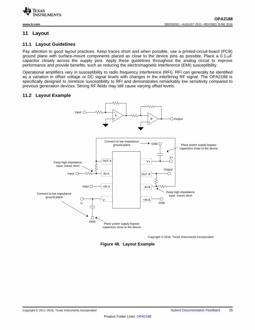
11 Layout
11.1 Layout GuidelinesPay attention to good layout practices. Keep traces short and when possible, use a printed-circuit-board (PCB)ground plane with surface-mount components placed as close to the device pins as possible. Place a 0.1-μFcapacitor closely across the supply pins. Apply these guidelines throughout the analog circuit to improveperformance and provide benefits, such as reducing the electromagnetic interference (EMI) susceptibility.
Operational amplifiers vary in susceptibility to radio frequency interference (RFI). RFI can generally be identifiedas a variation in offset voltage or DC signal levels with changes in the interfering RF signal. The OPA2188 isspecifically designed to minimize susceptibility to RFI and demonstrates remarkably low sensitivity compared toprevious generation devices. Strong RF fields may still cause varying offset levels.
11.2 Layout Example
Figure 48. Layout Example
26
OPA2188SBOS525C –AUGUST 2011–REVISED JUNE 2016 www.ti.com
Product Folder Links: OPA2188
Submit Documentation Feedback Copyright © 2011–2016, Texas Instruments Incorporated
12 Device and Documentation Support
12.1 Device Support
12.1.1 Development Support
12.1.1.1 TINA-TI™ (Free Software Download)TINA™ is a simple, powerful, and easy-to-use circuit simulation program based on a SPICE engine. TINA-TI™ isa free, fully-functional version of the TINA software, preloaded with a library of macro models in addition to arange of both passive and active models. TINA-TI provides all the conventional dc, transient, and frequencydomain analysis of SPICE, as well as additional design capabilities.
Available as a free download from the Analog eLab Design Center, TINA-TI offers extensive post-processingcapability that allows users to format results in a variety of ways. Virtual instruments offer the ability to selectinput waveforms and probe circuit nodes, voltages, and waveforms, creating a dynamic quick-start tool.
NOTEThese files require that either the TINA software (from DesignSoft™) or TINA-TI softwarebe installed. Download the free TINA-TI software from the TINA-TI folder.
12.1.1.2 DIP Adapter EVMThe DIP Adapter EVM tool provides an easy, low-cost way to prototype small surface mount ICs. The evaluationtool these TI packages: D or U (SOIC-8), PW (TSSOP-8), DGK (MSOP-8), DBV (SOT23-6, SOT23-5 andSOT23-3), DCK (SC70-6 and SC70-5), and DRL (SOT563-6). The DIP Adapter EVM may also be used withterminal strips or may be wired directly to existing circuits.
12.1.1.3 Universal Op Amp EVMThe Universal Op Amp EVM is a series of general-purpose, blank circuit boards that simplify prototyping circuitsfor a variety of IC package types. The evaluation module board design allows many different circuits to beconstructed easily and quickly. Five models are offered, with each model intended for a specific package type.PDIP, SOIC, MSOP, TSSOP and SOT23 packages are all supported.
NOTEThese boards are unpopulated, so users must provide their own ICs. TI recommendsrequesting several op amp device samples when ordering the Universal Op Amp EVM.
12.1.1.4 TI Precision DesignsTI Precision Designs are analog solutions created by TI’s precision analog applications experts and offer thetheory of operation, component selection, simulation, complete PCB schematic and layout, bill of materials, andmeasured performance of many useful circuits. TI Precision Designs are available online athttp://www.ti.com/ww/en/analog/precision-designs/.
12.1.1.5 WEBENCH® Filter DesignerWEBENCH® Filter Designer is a simple, powerful, and easy-to-use active filter design program. The WEBENCHFilter Designer lets you create optimized filter designs using a selection of TI operational amplifiers and passivecomponents from TI's vendor partners.
Available as a web-based tool from the WEBENCH® Design Center, WEBENCH® Filter Designer allows you todesign, optimize, and simulate complete multistage active filter solutions within minutes.
27
OPA2188www.ti.com SBOS525C –AUGUST 2011–REVISED JUNE 2016
Product Folder Links: OPA2188
Submit Documentation FeedbackCopyright © 2011–2016, Texas Instruments Incorporated
12.2 Documentation Support
12.2.1 Related DocumentationThe following documents are relevant to using the OPA2188, and recommended for reference. All are availablefor download at www.ti.com unless otherwise noted.• EMI Rejection Ratio of Operational Amplifiers.• Feedback Plots Define Op Amp AC Performance• Op Amp Performance Analysis.• Single-Supply Operation of Operational Amplifiers• Tuning in Amplifiers.
12.3 Receiving Notification of Documentation UpdatesTo receive notification of documentation updates, navigate to the device product folder on ti.com. In the upperright corner, click on Alert me to register and receive a weekly digest of any product information that haschanged. For change details, review the revision history included in any revised document.
12.4 Community ResourceThe following links connect to TI community resources. Linked contents are provided "AS IS" by the respectivecontributors. They do not constitute TI specifications and do not necessarily reflect TI's views; see TI's Terms ofUse.
TI E2E™ Online Community TI's Engineer-to-Engineer (E2E) Community. Created to foster collaborationamong engineers. At e2e.ti.com, you can ask questions, share knowledge, explore ideas and helpsolve problems with fellow engineers.
Design Support TI's Design Support Quickly find helpful E2E forums along with design support tools andcontact information for technical support.
12.5 TrademarksTINA-TI, E2E are trademarks of Texas Instruments.WEBENCH is a registered trademark of Texas Instruments.TINA, DesignSoft are trademarks of DesignSoft, Inc.All other trademarks are the property of their respective owners.
12.6 Electrostatic Discharge CautionThis integrated circuit can be damaged by ESD. Texas Instruments recommends that all integrated circuits be handled withappropriate precautions. Failure to observe proper handling and installation procedures can cause damage.
ESD damage can range from subtle performance degradation to complete device failure. Precision integrated circuits may be moresusceptible to damage because very small parametric changes could cause the device not to meet its published specifications.
12.7 GlossarySLYZ022 — TI Glossary.
This glossary lists and explains terms, acronyms, and definitions.
13 Mechanical, Packaging, and Orderable InformationThe following pages include mechanical, packaging, and orderable information. This information is the mostcurrent data available for the designated devices. This data is subject to change without notice and revision ofthis document. For browser-based versions of this data sheet, refer to the left-hand navigation.
PACKAGE OPTION ADDENDUM
www.ti.com 29-Jan-2016
Addendum-Page 1
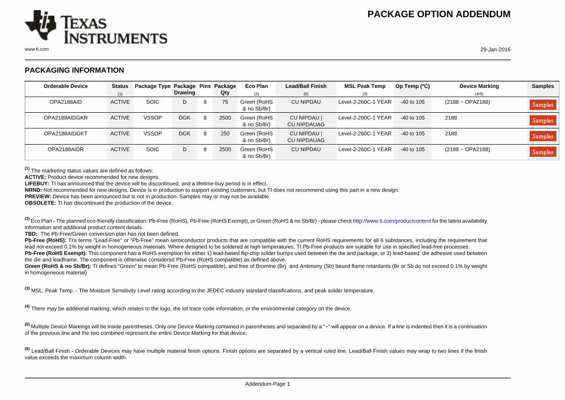
PACKAGING INFORMATION
Orderable Device Status(1)
Package Type PackageDrawing
Pins PackageQty
Eco Plan(2)
Lead/Ball Finish(6)
MSL Peak Temp(3)
Op Temp (°C) Device Marking(4/5)
Samples
OPA2188AID ACTIVE SOIC D 8 75 Green (RoHS& no Sb/Br)
CU NIPDAU Level-2-260C-1 YEAR -40 to 105 (2188 ~ OPA2188)
OPA2188AIDGKR ACTIVE VSSOP DGK 8 2500 Green (RoHS& no Sb/Br)
CU NIPDAU |CU NIPDAUAG
Level-2-260C-1 YEAR -40 to 105 2188
OPA2188AIDGKT ACTIVE VSSOP DGK 8 250 Green (RoHS& no Sb/Br)
CU NIPDAU |CU NIPDAUAG
Level-2-260C-1 YEAR -40 to 105 2188
OPA2188AIDR ACTIVE SOIC D 8 2500 Green (RoHS& no Sb/Br)
CU NIPDAU Level-2-260C-1 YEAR -40 to 105 (2188 ~ OPA2188)
(1) The marketing status values are defined as follows:ACTIVE: Product device recommended for new designs.LIFEBUY: TI has announced that the device will be discontinued, and a lifetime-buy period is in effect.NRND: Not recommended for new designs. Device is in production to support existing customers, but TI does not recommend using this part in a new design.PREVIEW: Device has been announced but is not in production. Samples may or may not be available.OBSOLETE: TI has discontinued the production of the device.
(2) Eco Plan - The planned eco-friendly classification: Pb-Free (RoHS), Pb-Free (RoHS Exempt), or Green (RoHS & no Sb/Br) - please check http://www.ti.com/productcontent for the latest availabilityinformation and additional product content details.TBD: The Pb-Free/Green conversion plan has not been defined.Pb-Free (RoHS): TI's terms "Lead-Free" or "Pb-Free" mean semiconductor products that are compatible with the current RoHS requirements for all 6 substances, including the requirement thatlead not exceed 0.1% by weight in homogeneous materials. Where designed to be soldered at high temperatures, TI Pb-Free products are suitable for use in specified lead-free processes.Pb-Free (RoHS Exempt): This component has a RoHS exemption for either 1) lead-based flip-chip solder bumps used between the die and package, or 2) lead-based die adhesive used betweenthe die and leadframe. The component is otherwise considered Pb-Free (RoHS compatible) as defined above.Green (RoHS & no Sb/Br): TI defines "Green" to mean Pb-Free (RoHS compatible), and free of Bromine (Br) and Antimony (Sb) based flame retardants (Br or Sb do not exceed 0.1% by weightin homogeneous material)
(3) MSL, Peak Temp. - The Moisture Sensitivity Level rating according to the JEDEC industry standard classifications, and peak solder temperature.
(4) There may be additional marking, which relates to the logo, the lot trace code information, or the environmental category on the device.
(5) Multiple Device Markings will be inside parentheses. Only one Device Marking contained in parentheses and separated by a "~" will appear on a device. If a line is indented then it is a continuationof the previous line and the two combined represent the entire Device Marking for that device.
(6) Lead/Ball Finish - Orderable Devices may have multiple material finish options. Finish options are separated by a vertical ruled line. Lead/Ball Finish values may wrap to two lines if the finishvalue exceeds the maximum column width.
PACKAGE OPTION ADDENDUM
www.ti.com 29-Jan-2016
Addendum-Page 2
Important Information and Disclaimer:The information provided on this page represents TI's knowledge and belief as of the date that it is provided. TI bases its knowledge and belief on informationprovided by third parties, and makes no representation or warranty as to the accuracy of such information. Efforts are underway to better integrate information from third parties. TI has taken andcontinues to take reasonable steps to provide representative and accurate information but may not have conducted destructive testing or chemical analysis on incoming materials and chemicals.TI and TI suppliers consider certain information to be proprietary, and thus CAS numbers and other limited information may not be available for release.
In no event shall TI's liability arising out of such information exceed the total purchase price of the TI part(s) at issue in this document sold by TI to Customer on an annual basis.
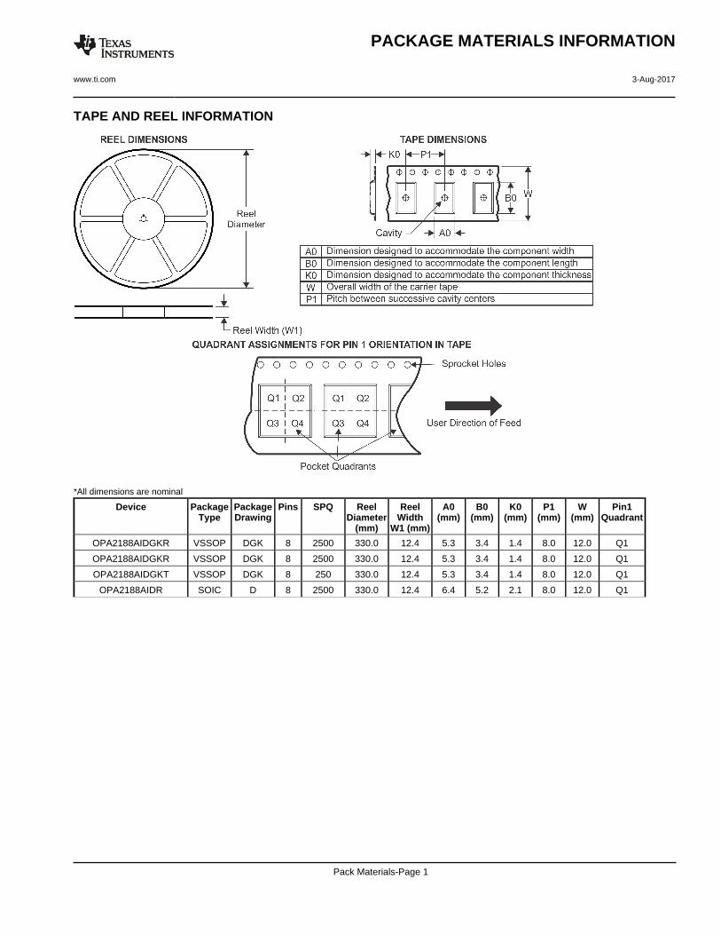
TAPE AND REEL INFORMATION
*All dimensions are nominal
Device PackageType
PackageDrawing
Pins SPQ ReelDiameter
(mm)
ReelWidth
W1 (mm)
A0(mm)
B0(mm)
K0(mm)
P1(mm)
W(mm)
Pin1Quadrant
OPA2188AIDGKR VSSOP DGK 8 2500 330.0 12.4 5.3 3.4 1.4 8.0 12.0 Q1
OPA2188AIDGKR VSSOP DGK 8 2500 330.0 12.4 5.3 3.4 1.4 8.0 12.0 Q1
OPA2188AIDGKT VSSOP DGK 8 250 330.0 12.4 5.3 3.4 1.4 8.0 12.0 Q1
OPA2188AIDR SOIC D 8 2500 330.0 12.4 6.4 5.2 2.1 8.0 12.0 Q1
PACKAGE MATERIALS INFORMATION
www.ti.com 3-Aug-2017
Pack Materials-Page 1
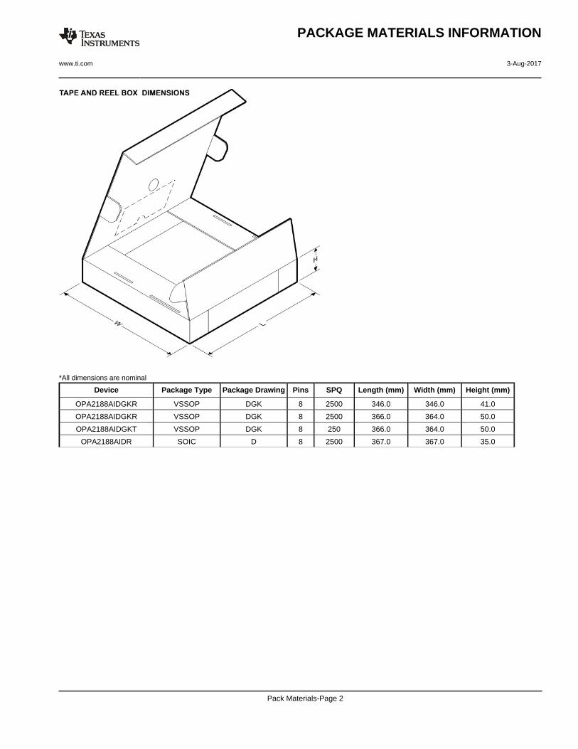
*All dimensions are nominal
Device Package Type Package Drawing Pins SPQ Length (mm) Width (mm) Height (mm)
OPA2188AIDGKR VSSOP DGK 8 2500 346.0 346.0 41.0
OPA2188AIDGKR VSSOP DGK 8 2500 366.0 364.0 50.0
OPA2188AIDGKT VSSOP DGK 8 250 366.0 364.0 50.0
OPA2188AIDR SOIC D 8 2500 367.0 367.0 35.0
PACKAGE MATERIALS INFORMATION
www.ti.com 3-Aug-2017
Pack Materials-Page 2
IMPORTANT NOTICE
Texas Instruments Incorporated (TI) reserves the right to make corrections, enhancements, improvements and other changes to itssemiconductor products and services per JESD46, latest issue, and to discontinue any product or service per JESD48, latest issue. Buyersshould obtain the latest relevant information before placing orders and should verify that such information is current and complete.TI’s published terms of sale for semiconductor products (http://www.ti.com/sc/docs/stdterms.htm) apply to the sale of packaged integratedcircuit products that TI has qualified and released to market. Additional terms may apply to the use or sale of other types of TI products andservices.Reproduction of significant portions of TI information in TI data sheets is permissible only if reproduction is without alteration and isaccompanied by all associated warranties, conditions, limitations, and notices. TI is not responsible or liable for such reproduceddocumentation. Information of third parties may be subject to additional restrictions. Resale of TI products or services with statementsdifferent from or beyond the parameters stated by TI for that product or service voids all express and any implied warranties for theassociated TI product or service and is an unfair and deceptive business practice. TI is not responsible or liable for any such statements.Buyers and others who are developing systems that incorporate TI products (collectively, “Designers”) understand and agree that Designersremain responsible for using their independent analysis, evaluation and judgment in designing their applications and that Designers havefull and exclusive responsibility to assure the safety of Designers' applications and compliance of their applications (and of all TI productsused in or for Designers’ applications) with all applicable regulations, laws and other applicable requirements. Designer represents that, withrespect to their applications, Designer has all the necessary expertise to create and implement safeguards that (1) anticipate dangerousconsequences of failures, (2) monitor failures and their consequences, and (3) lessen the likelihood of failures that might cause harm andtake appropriate actions. Designer agrees that prior to using or distributing any applications that include TI products, Designer willthoroughly test such applications and the functionality of such TI products as used in such applications.TI’s provision of technical, application or other design advice, quality characterization, reliability data or other services or information,including, but not limited to, reference designs and materials relating to evaluation modules, (collectively, “TI Resources”) are intended toassist designers who are developing applications that incorporate TI products; by downloading, accessing or using TI Resources in anyway, Designer (individually or, if Designer is acting on behalf of a company, Designer’s company) agrees to use any particular TI Resourcesolely for this purpose and subject to the terms of this Notice.TI’s provision of TI Resources does not expand or otherwise alter TI’s applicable published warranties or warranty disclaimers for TIproducts, and no additional obligations or liabilities arise from TI providing such TI Resources. TI reserves the right to make corrections,enhancements, improvements and other changes to its TI Resources. TI has not conducted any testing other than that specificallydescribed in the published documentation for a particular TI Resource.Designer is authorized to use, copy and modify any individual TI Resource only in connection with the development of applications thatinclude the TI product(s) identified in such TI Resource. NO OTHER LICENSE, EXPRESS OR IMPLIED, BY ESTOPPEL OR OTHERWISETO ANY OTHER TI INTELLECTUAL PROPERTY RIGHT, AND NO LICENSE TO ANY TECHNOLOGY OR INTELLECTUAL PROPERTYRIGHT OF TI OR ANY THIRD PARTY IS GRANTED HEREIN, including but not limited to any patent right, copyright, mask work right, orother intellectual property right relating to any combination, machine, or process in which TI products or services are used. Informationregarding or referencing third-party products or services does not constitute a license to use such products or services, or a warranty orendorsement thereof. Use of TI Resources may require a license from a third party under the patents or other intellectual property of thethird party, or a license from TI under the patents or other intellectual property of TI.TI RESOURCES ARE PROVIDED “AS IS” AND WITH ALL FAULTS. TI DISCLAIMS ALL OTHER WARRANTIES ORREPRESENTATIONS, EXPRESS OR IMPLIED, REGARDING RESOURCES OR USE THEREOF, INCLUDING BUT NOT LIMITED TOACCURACY OR COMPLETENESS, TITLE, ANY EPIDEMIC FAILURE WARRANTY AND ANY IMPLIED WARRANTIES OFMERCHANTABILITY, FITNESS FOR A PARTICULAR PURPOSE, AND NON-INFRINGEMENT OF ANY THIRD PARTY INTELLECTUALPROPERTY RIGHTS. TI SHALL NOT BE LIABLE FOR AND SHALL NOT DEFEND OR INDEMNIFY DESIGNER AGAINST ANY CLAIM,INCLUDING BUT NOT LIMITED TO ANY INFRINGEMENT CLAIM THAT RELATES TO OR IS BASED ON ANY COMBINATION OFPRODUCTS EVEN IF DESCRIBED IN TI RESOURCES OR OTHERWISE. IN NO EVENT SHALL TI BE LIABLE FOR ANY ACTUAL,DIRECT, SPECIAL, COLLATERAL, INDIRECT, PUNITIVE, INCIDENTAL, CONSEQUENTIAL OR EXEMPLARY DAMAGES INCONNECTION WITH OR ARISING OUT OF TI RESOURCES OR USE THEREOF, AND REGARDLESS OF WHETHER TI HAS BEENADVISED OF THE POSSIBILITY OF SUCH DAMAGES.Unless TI has explicitly designated an individual product as meeting the requirements of a particular industry standard (e.g., ISO/TS 16949and ISO 26262), TI is not responsible for any failure to meet such industry standard requirements.Where TI specifically promotes products as facilitating functional safety or as compliant with industry functional safety standards, suchproducts are intended to help enable customers to design and create their own applications that meet applicable functional safety standardsand requirements. Using products in an application does not by itself establish any safety features in the application. Designers mustensure compliance with safety-related requirements and standards applicable to their applications. Designer may not use any TI products inlife-critical medical equipment unless authorized officers of the parties have executed a special contract specifically governing such use.Life-critical medical equipment is medical equipment where failure of such equipment would cause serious bodily injury or death (e.g., lifesupport, pacemakers, defibrillators, heart pumps, neurostimulators, and implantables). Such equipment includes, without limitation, allmedical devices identified by the U.S. Food and Drug Administration as Class III devices and equivalent classifications outside the U.S.TI may expressly designate certain products as completing a particular qualification (e.g., Q100, Military Grade, or Enhanced Product).Designers agree that it has the necessary expertise to select the product with the appropriate qualification designation for their applicationsand that proper product selection is at Designers’ own risk. Designers are solely responsible for compliance with all legal and regulatoryrequirements in connection with such selection.Designer will fully indemnify TI and its representatives against any damages, costs, losses, and/or liabilities arising out of Designer’s non-compliance with the terms and provisions of this Notice.
Mailing Address: Texas Instruments, Post Office Box 655303, Dallas, Texas 75265Copyright © 2017, Texas Instruments Incorporated