N-channel 800 V, 0.95 typ., 3.6 A MDmesh K5 Power ...July 2017 DocID025551 Rev 2 1/17 This is...
17
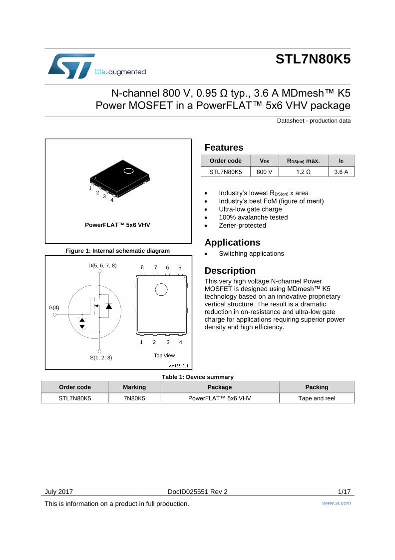
July 2017 DocID025551 Rev 2 1/17 This is information on a product in full production. www.st.com STL7N80K5 N-channel 800 V, 0.95 Ω typ., 3.6 A MDmesh™ K5 Power MOSFET in a PowerFLAT™ 5x6 VHV package Datasheet - production data Figure 1: Internal schematic diagram Features Order code VDS RDS(on) max. ID STL7N80K5 800 V 1.2 Ω 3.6 A Industry’s lowest RDS(on) x area Industry’s best FoM (figure of merit) Ultra-low gate charge 100% avalanche tested Zener-protected Applications Switching applications Description This very high voltage N-channel Power MOSFET is designed using MDmesh™ K5 technology based on an innovative proprietary vertical structure. The result is a dramatic reduction in on-resistance and ultra-low gate charge for applications requiring superior power density and high efficiency. Table 1: Device summary Order code Marking Package Packing STL7N80K5 7N80K5 PowerFLAT™ 5x6 VHV Tape and reel 1 2 3 4 PowerFLAT™ 5x6 VHV 5 6 7 8 1 2 3 4 Top View D(5, 6, 7, 8) G(4) S(1, 2, 3)
Transcript of N-channel 800 V, 0.95 typ., 3.6 A MDmesh K5 Power ...July 2017 DocID025551 Rev 2 1/17 This is...
July 2017 DocID025551 Rev 2 1/17
This is information on a product in full production. www.st.com
STL7N80K5
N-channel 800 V, 0.95 Ω typ., 3.6 A MDmesh™ K5 Power MOSFET in a PowerFLAT™ 5x6 VHV package
Datasheet - production data
Figure 1: Internal schematic diagram
Features
Order code VDS RDS(on) max. ID
STL7N80K5 800 V 1.2 Ω 3.6 A
Industry’s lowest RDS(on) x area
Industry’s best FoM (figure of merit)
Ultra-low gate charge
100% avalanche tested
Zener-protected
Applications Switching applications
Description This very high voltage N-channel Power MOSFET is designed using MDmesh™ K5 technology based on an innovative proprietary vertical structure. The result is a dramatic reduction in on-resistance and ultra-low gate charge for applications requiring superior power density and high efficiency.
Table 1: Device summary
Order code Marking Package Packing
STL7N80K5 7N80K5 PowerFLAT™ 5x6 VHV Tape and reel
12
34
PowerFLAT™ 5x6 VHV
5678
1 2 3 4
Top View
D(5, 6, 7, 8)
G(4)
S(1, 2, 3)
Contents STL7N80K5
2/17 DocID025551 Rev 2
Contents
1 Electrical ratings ............................................................................. 3
2 Electrical characteristics ................................................................ 4
2.1 Electrical characteristics (curves) ...................................................... 6
3 Test circuits ..................................................................................... 9
4 Package information ..................................................................... 10
4.1 PowerFLAT™ 5x6 VHV package information ................................. 11
4.2 PowerFLAT™ 5x6 packing information ........................................... 14
5 Revision history ............................................................................ 16
STL7N80K5 Electrical ratings
DocID025551 Rev 2 3/17
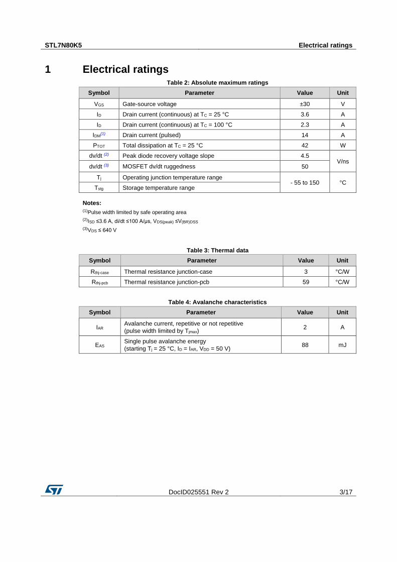
1 Electrical ratings Table 2: Absolute maximum ratings
Symbol Parameter Value Unit
VGS Gate-source voltage ±30 V
ID Drain current (continuous) at TC = 25 °C 3.6 A
ID Drain current (continuous) at TC = 100 °C 2.3 A
IDM(1) Drain current (pulsed) 14 A
PTOT Total dissipation at TC = 25 °C 42 W
dv/dt (2) Peak diode recovery voltage slope 4.5 V/ns
dv/dt (3) MOSFET dv/dt ruggedness 50
Tj Operating junction temperature range - 55 to 150 °C
Tstg Storage temperature range
Notes:
(1)Pulse width limited by safe operating area (2)ISD ≤3.6 A, di/dt ≤100 A/μs, VDS(peak) ≤V(BR)DSS (3)VDS ≤ 640 V
Table 3: Thermal data
Symbol Parameter Value Unit
Rthj-case Thermal resistance junction-case 3 °C/W
Rthj-pcb Thermal resistance junction-pcb 59 °C/W
Table 4: Avalanche characteristics
Symbol Parameter Value Unit
IAR Avalanche current, repetitive or not repetitive
(pulse width limited by Tjmax) 2 A
EAS Single pulse avalanche energy
(starting Tj = 25 °C, ID = IAR, VDD = 50 V) 88 mJ
Electrical characteristics STL7N80K5
4/17 DocID025551 Rev 2
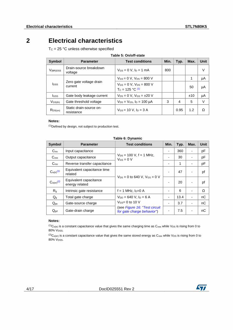
2 Electrical characteristics
TC = 25 °C unless otherwise specified
Table 5: On/off-state
Symbol Parameter Test conditions Min. Typ. Max. Unit
V(BR)DSS Drain-source breakdown
voltage VGS = 0 V, ID = 1 mA 800
V
IDSS Zero gate voltage drain
current
VGS = 0 V, VDS = 800 V
1 µA
VGS = 0 V, VDS = 800 V
TC = 125 °C (1) 50 µA
IGSS Gate body leakage current VDS = 0 V, VGS = ±20 V
±10 µA
VGS(th) Gate threshold voltage VDS = VGS, ID = 100 µA 3 4 5 V
RDS(on) Static drain-source on-
resistance VGS = 10 V, ID = 3 A
0.95 1.2 Ω
Notes:
(1)Defined by design, not subject to production test.
Table 6: Dynamic
Symbol Parameter Test conditions Min. Typ. Max. Unit
Ciss Input capacitance
VDS = 100 V, f = 1 MHz,
VGS = 0 V
- 360 - pF
Coss Output capacitance - 30 - pF
Crss Reverse transfer capacitance - 1 - pF
Co(tr)(1)
Equivalent capacitance time
related VDS = 0 to 640 V, VGS = 0 V
- 47 - pf
Co(er)(2)
Equivalent capacitance
energy related - 20 - pf
Rg Intrinsic gate resistance f = 1 MHz, ID=0 A - 6 - Ω
Qg Total gate charge VDD = 640 V, ID = 6 A
VGS= 0 to 10 V
(see Figure 16: "Test circuit for gate charge behavior")
- 13.4 - nC
Qgs Gate-source charge - 3.7 - nC
Qgd Gate-drain charge - 7.5 - nC
Notes:
(1)Co(tr) is a constant capacitance value that gives the same charging time as Coss while VDS is rising from 0 to
80% VDSS. (2)Co(er) is a constant capacitance value that gives the same stored energy as Coss while VDS is rising from 0 to
80% VDSS.
STL7N80K5 Electrical characteristics
DocID025551 Rev 2 5/17
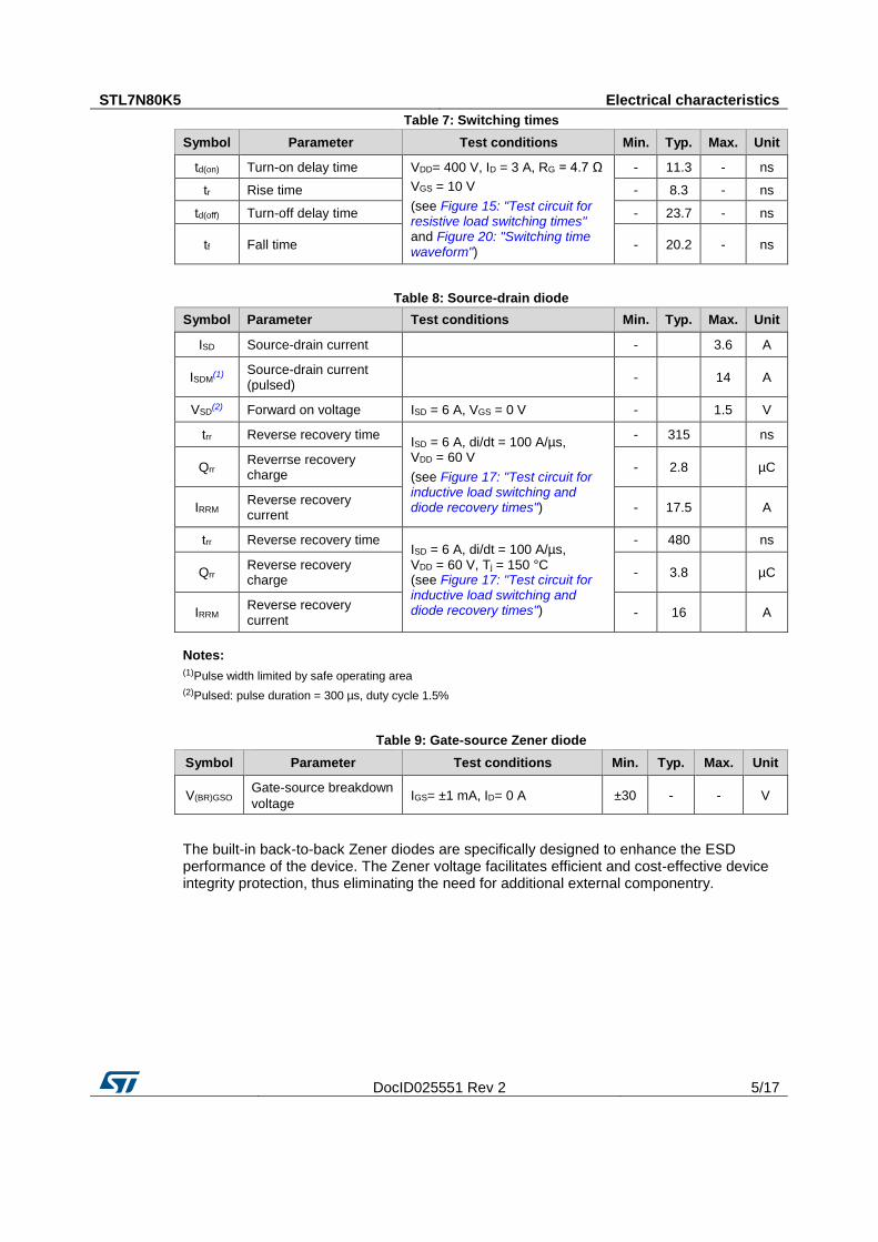
Table 7: Switching times
Symbol Parameter Test conditions Min. Typ. Max. Unit
td(on) Turn-on delay time VDD= 400 V, ID = 3 A, RG = 4.7 Ω
VGS = 10 V
(see Figure 15: "Test circuit for resistive load switching times" and Figure 20: "Switching time waveform")
- 11.3 - ns
tr Rise time - 8.3 - ns
td(off) Turn-off delay time - 23.7 - ns
tf Fall time - 20.2 - ns
Table 8: Source-drain diode
Symbol Parameter Test conditions Min. Typ. Max. Unit
ISD Source-drain current
-
3.6 A
ISDM(1)
Source-drain current (pulsed)
-
14 A
VSD(2) Forward on voltage ISD = 6 A, VGS = 0 V -
1.5 V
trr Reverse recovery time ISD = 6 A, di/dt = 100 A/µs, VDD = 60 V
(see Figure 17: "Test circuit for inductive load switching and diode recovery times")
- 315
ns
Qrr Reverrse recovery charge
- 2.8
µC
IRRM Reverse recovery current
- 17.5
A
trr Reverse recovery time ISD = 6 A, di/dt = 100 A/µs, VDD = 60 V, Tj = 150 °C (see Figure 17: "Test circuit for inductive load switching and diode recovery times")
- 480
ns
Qrr Reverse recovery charge
- 3.8
µC
IRRM Reverse recovery current
- 16
A
Notes:
(1)Pulse width limited by safe operating area (2)Pulsed: pulse duration = 300 µs, duty cycle 1.5%
Table 9: Gate-source Zener diode
Symbol Parameter Test conditions Min. Typ. Max. Unit
V(BR)GSO Gate-source breakdown
voltage IGS= ±1 mA, ID= 0 A ±30 - - V
The built-in back-to-back Zener diodes are specifically designed to enhance the ESD performance of the device. The Zener voltage facilitates efficient and cost-effective device integrity protection, thus eliminating the need for additional external componentry.
Electrical characteristics STL7N80K5
6/17 DocID025551 Rev 2
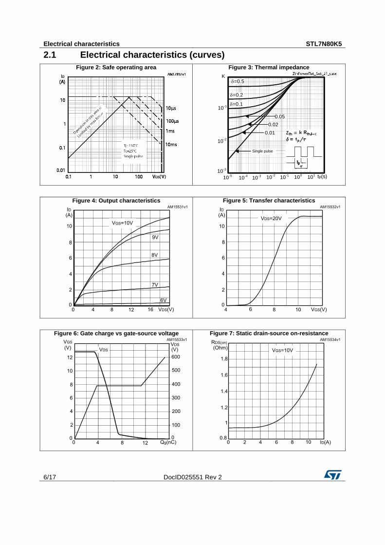
2.1 Electrical characteristics (curves)
Figure 2: Safe operating area
Figure 3: Thermal impedance
Figure 4: Output characteristics
Figure 5: Transfer characteristics
Figure 6: Gate charge vs gate-source voltage
Figure 7: Static drain-source on-resistance
Single pulse
d=0.5
0.05
0.02
0.01
d=0.2
d=0.1
K
10 tp(s)-410
-3
10-2
10-1
10-5
10-3
10-2
10-1 10
0
c
101
STL7N80K5 Electrical characteristics
DocID025551 Rev 2 7/17
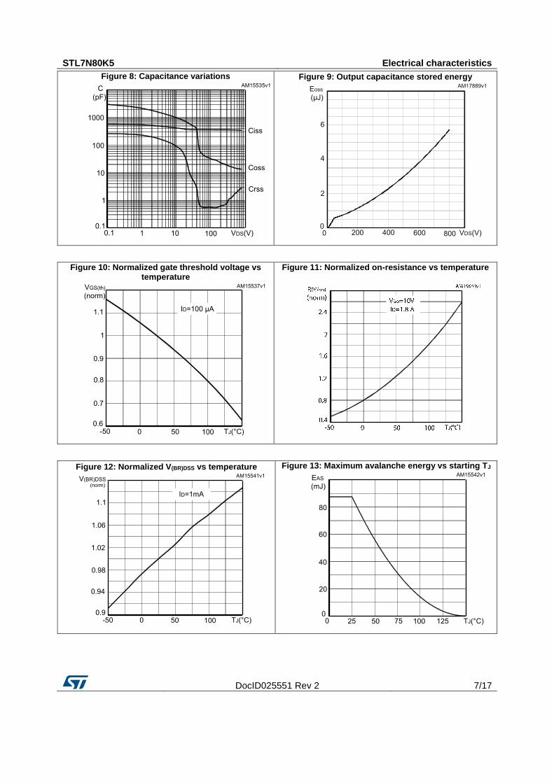
Figure 8: Capacitance variations
Figure 9: Output capacitance stored energy
Figure 10: Normalized gate threshold voltage vs temperature
Figure 11: Normalized on-resistance vs temperature
Figure 12: Normalized V(BR)DSS vs temperature
Figure 13: Maximum avalanche energy vs starting TJ
Electrical characteristics STL7N80K5
8/17 DocID025551 Rev 2
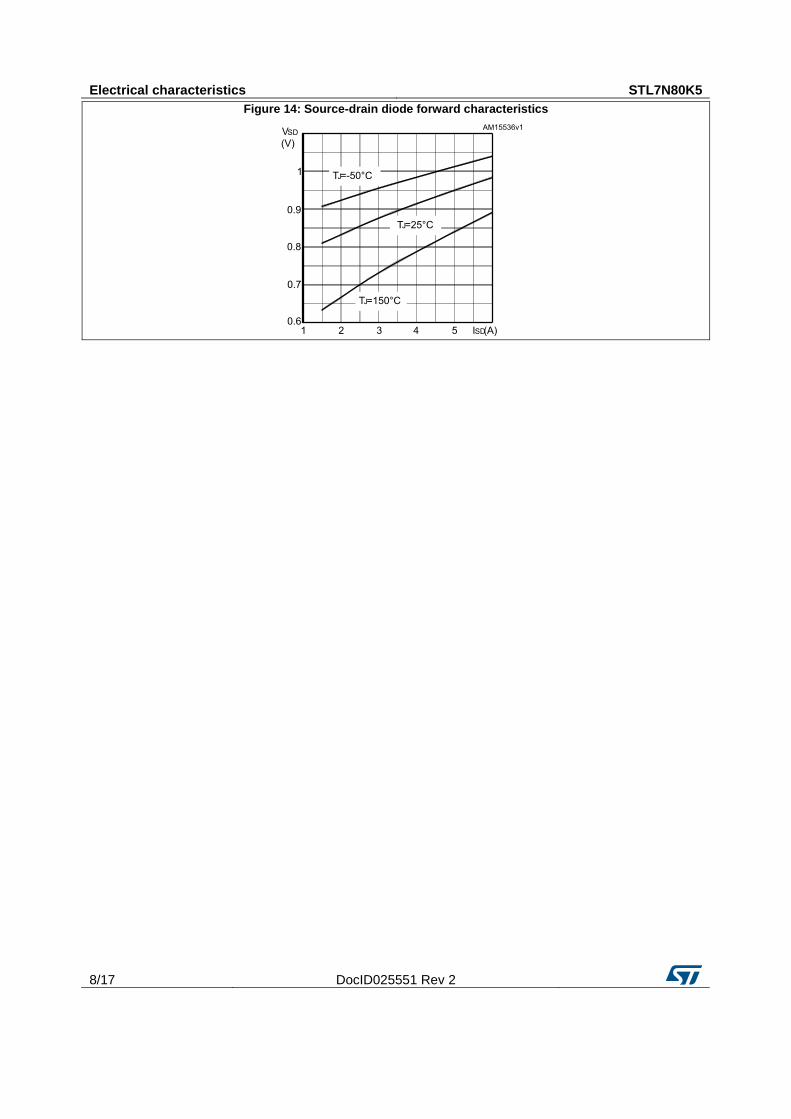
Figure 14: Source-drain diode forward characteristics
STL7N80K5 Test circuits
DocID025551 Rev 2 9/17
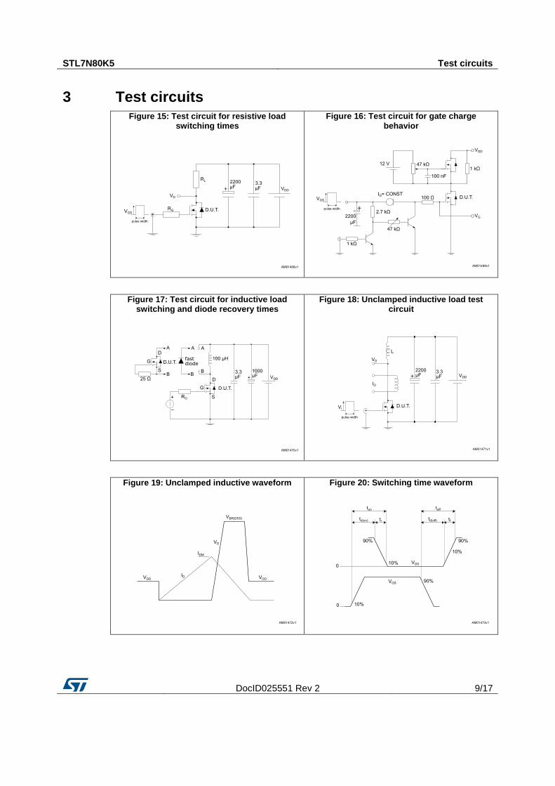
3 Test circuits Figure 15: Test circuit for resistive load
switching times
Figure 16: Test circuit for gate charge behavior
Figure 17: Test circuit for inductive load switching and diode recovery times
Figure 18: Unclamped inductive load test circuit
Figure 19: Unclamped inductive waveform
Figure 20: Switching time waveform
Package information STL7N80K5
10/17 DocID025551 Rev 2
4 Package information
In order to meet environmental requirements, ST offers these devices in different grades of ECOPACK® packages, depending on their level of environmental compliance. ECOPACK® specifications, grade definitions and product status are available at: www.st.com. ECOPACK® is an ST trademark.
STL7N80K5 Package information
DocID025551 Rev 2 11/17
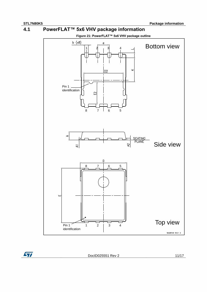
4.1 PowerFLAT™ 5x6 VHV package information
Figure 21: PowerFLAT™ 5x6 VHV package outline
Bottom view
Side view
Top view
1 2 3 4
Pin 1
identification
8 7 6 5
8 7 6 5
1 2 3 4Pin 1
identification
Package information STL7N80K5
12/17 DocID025551 Rev 2
Table 10: PowerFLAT™ 5x6 VHV package mechanical data
Dim. mm
Min. Typ. Max.
A 0.80
1.00
A1 0.02
0.05
A2
0.25
b 0.30
0.50
D 5.00 5.20 5.40
E 5.95 6.15 6.35
D2 4.30 4.40 4.50
E2 2.40 2.50 2.60
e
1.27
L 0.50 0.55 0.60
K 2.60 2.70 2.80
STL7N80K5 Package information
DocID025551 Rev 2 13/17
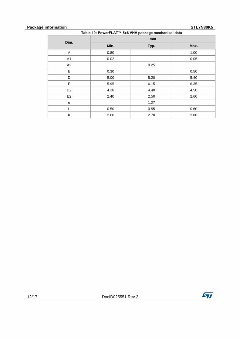
Figure 22: PowerFLAT™ 5x6 VHV recommended footprint (dimensions are in mm)
8368144_REV_3_footprint
Package information STL7N80K5
14/17 DocID025551 Rev 2
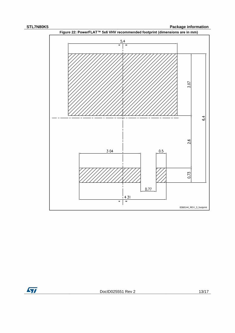
4.2 PowerFLAT™ 5x6 packing information
Figure 23: PowerFLAT™ 5x6 tape (dimensions are in mm)
Figure 24: PowerFLAT™ 5x6 package orientation in carrier tape
(I) Measured from centreline of sprocket hole
to centreline of pocket.
(II) Cumulative tolerance of 10 sprocket
holes is ±0.20.
(III) Measured from centreline of sprocket
hole to centreline of pocket
Base and bulk quantity 3000 pcs
All dimensions are in millimeters
8234350_Tape_rev_C
STL7N80K5 Package information
DocID025551 Rev 2 15/17
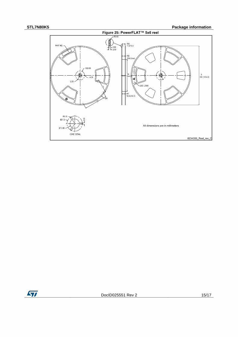
Figure 25: PowerFLAT™ 5x6 reel
Revision history STL7N80K5
16/17 DocID025551 Rev 2
5 Revision history Table 11: Document revision history
Date Revision Changes
19-Nov-2013 1 First release.
07-Jul-2017 2
Modified Table 9: "Gate-source Zener diode"
Modified Figure 3: "Thermal impedance".
Updated Section 4: "Package information".
Minor text changes.
STL7N80K5
DocID025551 Rev 2 17/17
IMPORTANT NOTICE – PLEASE READ CAREFULLY
STMicroelectronics NV and its subsidiaries (“ST”) reserve the right to make changes, corrections, enhancements, modifications , and improvements to ST products and/or to this document at any time without notice. Purchasers should obtain the latest relevant information on ST products before placing orders. ST products are sold pursuant to ST’s terms and conditions of sale in place at the time of order acknowledgement.
Purchasers are solely responsible for the choice, selection, and use of ST products and ST assumes no liability for application assistance or the design of Purchasers’ products.
No license, express or implied, to any intellectual property right is granted by ST herein.
Resale of ST products with provisions different from the information set forth herein shall void any warranty granted by ST for such product.
ST and the ST logo are trademarks of ST. All other product or service names are the property of their respective owners.
Information in this document supersedes and replaces information previously supplied in any prior versions of this document.
© 2017 STMicroelectronics – All rights reserved