MODEL ANALYSIS AND PARAMETER EXTRACTION FOR MOS CAPACITOR ... · Model Analysis and Parameter...
11
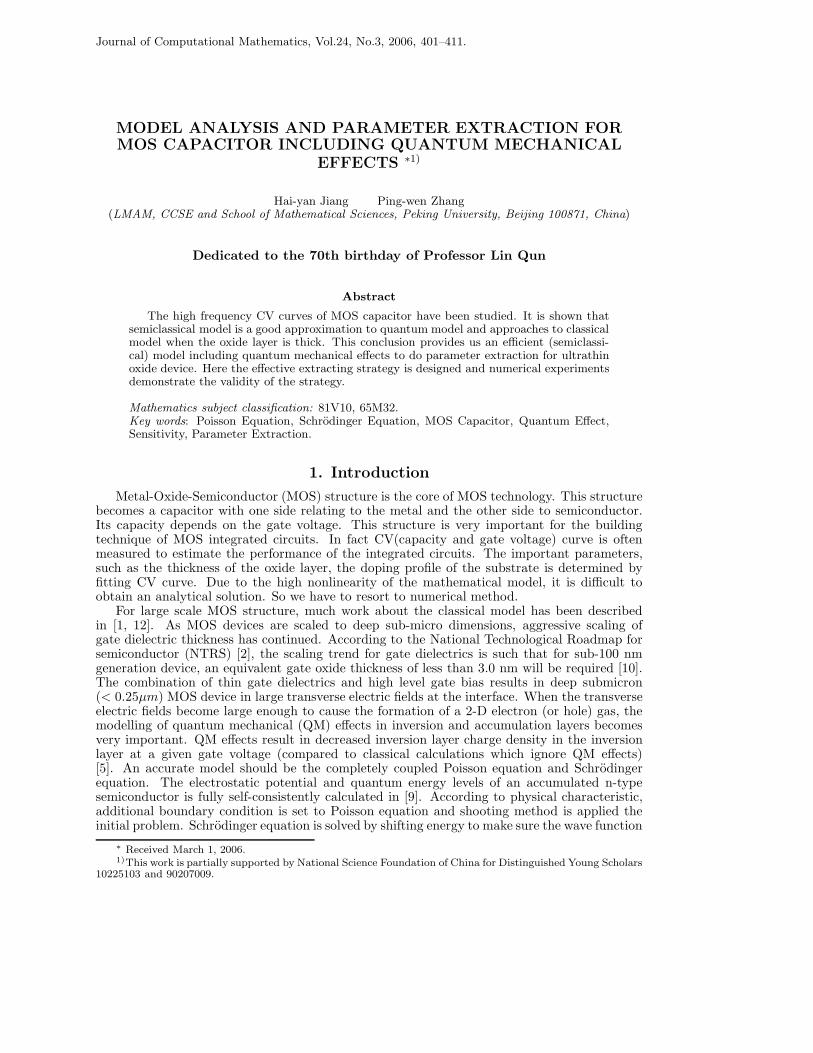
Journal of Computational Mathematics, Vol.24, No.3, 2006, 401–411. MODEL ANALYSIS AND PARAMETER EXTRACTION FOR MOS CAPACITOR INCLUDING QUANTUM MECHANICAL EFFECTS *1) Hai-yan Jiang Ping-wen Zhang (LMAM, CCSE and School of Mathematical Sciences, Peking University, Beijing 100871, China) Dedicated to the 70th birthday of Professor Lin Qun Abstract The high frequency CV curves of MOS capacitor have been studied. It is shown that semiclassical model is a good approximation to quantum model and approaches to classical model when the oxide layer is thick. This conclusion provides us an efficient (semiclassi- cal) model including quantum mechanical effects to do parameter extraction for ultrathin oxide device. Here the effective extracting strategy is designed and numerical experiments demonstrate the validity of the strategy. Mathematics subject classification: 81V10, 65M32. Key words: Poisson Equation, Schr¨odinger Equation, MOS Capacitor, Quantum Effect, Sensitivity, Parameter Extraction. 1. Introduction Metal-Oxide-Semiconductor (MOS) structure is the core of MOS technology. This structure becomes a capacitor with one side relating to the metal and the other side to semiconductor. Its capacity depends on the gate voltage. This structure is very important for the building technique of MOS integrated circuits. In fact CV(capacity and gate voltage) curve is often measured to estimate the performance of the integrated circuits. The important parameters, such as the thickness of the oxide layer, the doping profile of the substrate is determined by fitting CV curve. Due to the high nonlinearity of the mathematical model, it is difficult to obtain an analytical solution. So we have to resort to numerical method. For large scale MOS structure, much work about the classical model has been described in [1, 12]. As MOS devices are scaled to deep sub-micro dimensions, aggressive scaling of gate dielectric thickness has continued. According to the National Technological Roadmap for semiconductor (NTRS) [2], the scaling trend for gate dielectrics is such that for sub-100 nm generation device, an equivalent gate oxide thickness of less than 3.0 nm will be required [10]. The combination of thin gate dielectrics and high level gate bias results in deep submicron (< 0.25μm) MOS device in large transverse electric fields at the interface. When the transverse electric fields become large enough to cause the formation of a 2-D electron (or hole) gas, the modelling of quantum mechanical (QM) effects in inversion and accumulation layers becomes very important. QM effects result in decreased inversion layer charge density in the inversion layer at a given gate voltage (compared to classical calculations which ignore QM effects) [5]. An accurate model should be the completely coupled Poisson equation and Schr¨ odinger equation. The electrostatic potential and quantum energy levels of an accumulated n-type semiconductor is fully self-consistently calculated in [9]. According to physical characteristic, additional boundary condition is set to Poisson equation and shooting method is applied the initial problem. Schr¨ odinger equation is solved by shifting energy to make sure the wave function * Received March 1, 2006. 1) This work is partially supported by National Science Foundation of China for Distinguished Young Scholars 10225103 and 90207009.
Transcript of MODEL ANALYSIS AND PARAMETER EXTRACTION FOR MOS CAPACITOR ... · Model Analysis and Parameter...
Journal of Computational Mathematics, Vol.24, No.3, 2006, 401–411.
MODEL ANALYSIS AND PARAMETER EXTRACTION FORMOS CAPACITOR INCLUDING QUANTUM MECHANICAL
EFFECTS ∗1)
Hai-yan Jiang Ping-wen Zhang(LMAM, CCSE and School of Mathematical Sciences, Peking University, Beijing 100871, China)
Dedicated to the 70th birthday of Professor Lin Qun
Abstract
The high frequency CV curves of MOS capacitor have been studied. It is shown thatsemiclassical model is a good approximation to quantum model and approaches to classicalmodel when the oxide layer is thick. This conclusion provides us an efficient (semiclassi-cal) model including quantum mechanical effects to do parameter extraction for ultrathinoxide device. Here the effective extracting strategy is designed and numerical experimentsdemonstrate the validity of the strategy.
Mathematics subject classification: 81V10, 65M32.Key words: Poisson Equation, Schrodinger Equation, MOS Capacitor, Quantum Effect,Sensitivity, Parameter Extraction.
1. Introduction
Metal-Oxide-Semiconductor (MOS) structure is the core of MOS technology. This structurebecomes a capacitor with one side relating to the metal and the other side to semiconductor.Its capacity depends on the gate voltage. This structure is very important for the buildingtechnique of MOS integrated circuits. In fact CV(capacity and gate voltage) curve is oftenmeasured to estimate the performance of the integrated circuits. The important parameters,such as the thickness of the oxide layer, the doping profile of the substrate is determined byfitting CV curve. Due to the high nonlinearity of the mathematical model, it is difficult toobtain an analytical solution. So we have to resort to numerical method.
For large scale MOS structure, much work about the classical model has been describedin [1, 12]. As MOS devices are scaled to deep sub-micro dimensions, aggressive scaling ofgate dielectric thickness has continued. According to the National Technological Roadmap forsemiconductor (NTRS) [2], the scaling trend for gate dielectrics is such that for sub-100 nmgeneration device, an equivalent gate oxide thickness of less than 3.0 nm will be required [10].The combination of thin gate dielectrics and high level gate bias results in deep submicron(< 0.25µm) MOS device in large transverse electric fields at the interface. When the transverseelectric fields become large enough to cause the formation of a 2-D electron (or hole) gas, themodelling of quantum mechanical (QM) effects in inversion and accumulation layers becomesvery important. QM effects result in decreased inversion layer charge density in the inversionlayer at a given gate voltage (compared to classical calculations which ignore QM effects)[5]. An accurate model should be the completely coupled Poisson equation and Schrodingerequation. The electrostatic potential and quantum energy levels of an accumulated n-typesemiconductor is fully self-consistently calculated in [9]. According to physical characteristic,additional boundary condition is set to Poisson equation and shooting method is applied theinitial problem. Schrodinger equation is solved by shifting energy to make sure the wave function
∗ Received March 1, 2006.1)This work is partially supported by National Science Foundation of China for Distinguished Young Scholars
10225103 and 90207009.
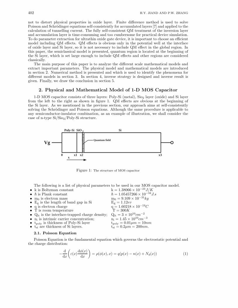
402 H.Y. JIAND AND P.W. ZHANG
not to distort physical properties in oxide layer. Finite difference method is used to solvePoisson and Schrodinger equations self-consistently for accumulated layers [7] and applied to thecalculation of tunnelling current. The fully self-consistent QM treatment of the inversion layerand accumulation layer is time-consuming and too cumbersome for practical device simulation.To do parameter extraction for ultrathin oxide gate device, it is important to choose an efficientmodel including QM effects. QM effects is obvious only in the potential well at the interfaceof oxide layer and Si layer, so it is not necessary to include QM effect in the global region. Inthis paper, the semiclassical model is presented, quantum region is located at the beginning ofthe Si layer, which is set large enough to include QM effects and other regions are consideredclassically.
The main purpose of this paper is to analyze the different scale mathematical models andextract important parameters. The physical model and mathematical models are introducedin section 2. Numerical method is presented and which is used to identify the phenomena fordifferent models in section 3. In section 4, inverse strategy is designed and inverse result isgiven. Finally, we draw the conclusion in section 5.
2. Physical and Mathematical Model of 1-D MOS Capacitor
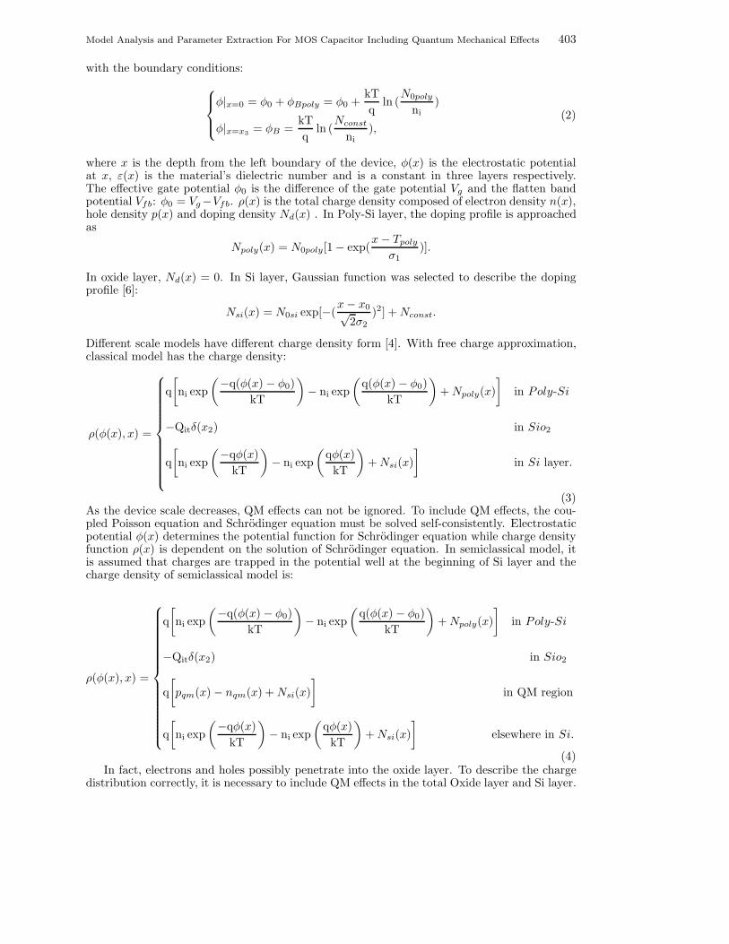
1-D MOS capacitor consists of three layers: Poly-Si (metal), Sio2 layer (oxide) and Si layerfrom the left to the right as shown in figure 1. QM effects are obvious at the beginning ofthe Si layer. As we mentioned in the previous section, our approach aims at self-consistentlysolving the Schrodinger and Poisson equations. Although the same procedure is applicable toany semiconductor-insulator combination, as an example of illustration, we shall consider thecase of n-type Si/Sio2/Poly-Si structure.
Vg
Poly-Si SiO 2 Si
x1 x2 0 x3 x
Quantum field
Figure 1: The structure of MOS capacitor
The following is a list of physical parameters to be used in our MOS capacitor model.• k is Boltzman constant k = 1.38066× 10⁻²³J/K• ~ is Plank constant ~ = 1.05457266× 10⁻³⁴J.s• m0 is electron mass m0 = 9.109 × 10⁻³¹kg• Eg is the length of band gap in Si Eg = 1.12ev• q is electron charge q = 1.60218× 10⁻¹⁹C• T is room temperature T = 300K• Qit is the interface-trapped charge density; Qit = 3 × 1010cm−2
• ni is intrinsic carrier concentration; ni = 1.45 × 1010cm−3
• tpoly is thickness of Poly-Si layer tpoly = 0.01µm = 10nm• tsi are thickness of Si layers. tsi = 0.2µm = 200nm.
2.1. Poisson Equation
Poisson Equation is the fundamental equation which governs the electrostatic potential andthe charge distribution:
− d
dx
(
ε(x)dφ(x)
dx
)
= ρ(φ(x), x) = q(p(x) − n(x) +Nd(x)) (1)
Model Analysis and Parameter Extraction For MOS Capacitor Including Quantum Mechanical Effects 403
with the boundary conditions:
φ|x=0 = φ0 + φBpoly = φ0 +kT
qln (
N0poly
ni)
φ|x=x3= φB =
kT
qln (
Nconst
ni),
(2)
where x is the depth from the left boundary of the device, φ(x) is the electrostatic potentialat x, ε(x) is the material’s dielectric number and is a constant in three layers respectively.The effective gate potential φ0 is the difference of the gate potential Vg and the flatten bandpotential Vfb: φ0 = Vg−Vfb. ρ(x) is the total charge density composed of electron density n(x),hole density p(x) and doping density Nd(x) . In Poly-Si layer, the doping profile is approachedas
Npoly(x) = N0poly[1 − exp(x− Tpoly
σ1)].
In oxide layer, Nd(x) = 0. In Si layer, Gaussian function was selected to describe the dopingprofile [6]:
Nsi(x) = N0si exp[−(x− x0√
2σ2
)2] +Nconst.
Different scale models have different charge density form [4]. With free charge approximation,classical model has the charge density:
ρ(φ(x), x) =
q
[
ni exp
(−q(φ(x) − φ0)
kT
)
− ni exp
(
q(φ(x) − φ0)
kT
)
+Npoly(x)
]
in Poly-Si
−Qitδ(x2) in Sio2
q
[
ni exp
(−qφ(x)
kT
)
− ni exp
(
qφ(x)
kT
)
+Nsi(x)
]
in Si layer.
(3)As the device scale decreases, QM effects can not be ignored. To include QM effects, the cou-pled Poisson equation and Schrodinger equation must be solved self-consistently. Electrostaticpotential φ(x) determines the potential function for Schrodinger equation while charge densityfunction ρ(x) is dependent on the solution of Schrodinger equation. In semiclassical model, itis assumed that charges are trapped in the potential well at the beginning of Si layer and thecharge density of semiclassical model is:
ρ(φ(x), x) =
q
[
ni exp
(−q(φ(x) − φ0)
kT
)
− ni exp
(
q(φ(x) − φ0)
kT
)
+Npoly(x)
]
in Poly-Si
−Qitδ(x2) in Sio2
q
[
pqm(x) − nqm(x) +Nsi(x)
]
in QM region
q
[
ni exp
(−qφ(x)
kT
)
− ni exp
(
qφ(x)
kT
)
+Nsi(x)
]
elsewhere in Si.
(4)In fact, electrons and holes possibly penetrate into the oxide layer. To describe the charge
distribution correctly, it is necessary to include QM effects in the total Oxide layer and Si layer.
404 H.Y. JIAND AND P.W. ZHANG
So the quantum model’s charge density is:
ρ(φ(x), x) =
q
[
ni exp
(−q(φ(x) − φ0)
kT
)
− ni exp
(
q(φ(x) − φ0)
kT
)
+Npoly(x)
]
in Poly-Si
q
[
pqm(x) − nqm(x) +Nd(x)
]
in Sio2 and Si
(5)pqm(x) and nqm(x) are the hole density and electron density of the quantum region with theindex qm to denote quantum effect. Before pqm(x) and nqm(x) are computed, stationarySchrodinger equation must be considered.
2.2. Schrodinger Equation
For semiclassical model, it is assumed that the potential barrier at the interface of oxide layerand Si layer is infinite and charge are trapped in the narrow potential well. So it is reasonableto set zero boundary condition to Schrodinger equation at quantum region boundary:
[
− ~2
2m∗
d2
dx2+ qV ∗(x)
]
ψj(x) = Ejψj(x)
ψj(x2) = 0
ψj(x2 + Lq) = 0
(6)
where Lq is the width of the quantum region. The barrier height is about 3.2ev for electronsand 4.8ev for holes at the interface of oxide layer and Si layer. Electrons and holes possiblypenetrate into oxide layer [8]. Thus, wave functions should penetrate into oxide layer. Completequantum model describes it correctly. The corresponding Schrodinger equation is:
[
− ~2
2m∗(x)
d2
dx2+ qV ∗(x)
]
ψj(x) = Ejψj(x)
ψj(x1) = 0
ψj(x3) = 0
(7)
The wave function and velocity are continuous at the interface of oxide layer and Si layer:
ψ(x−2 ) = ψ(x+2 )
1
mox
∂ψ(x−2 )
∂x=
1
msi
∂ψ(x+2 )
∂x.
m∗ is the effective mass of charge and space dependent (mox = 0.5m0 in oxide layer). V ∗(x) isthe potential function, linear dependent on static potential in oxide layer for quantum model.Index ∗ indicates different value of m∗ and V ∗(x) according to different charge (hole or electron)and different degeneration in Si.For electron,
V ∗(x) = Ve(x) =Eg
2q− (φ(x) − φB) Ve(x
−
2 ) = Ve(x+2 ) + 3.2.
For Hole,
V ∗(x) = Vh(x) =Eg
2q+ (φ(x) − φB) Vh(x−2 ) = Vh(x+
2 ) + 4.8.
The density state of 2-D electron (hole) gas is constant N(E) =m
π~2. Energy occupation is
governed by the Fermi-Dirac distribution f(E,EF , T ):
f(E,EF , T ) = [exp(E − EF
kT) + 1]−1.
Model Analysis and Parameter Extraction For MOS Capacitor Including Quantum Mechanical Effects 405
Thus, the density of charge per unit area is given by
n =
∫
N(E)f(E,EF , T )dE.
After computing Ej and ψj(x) and superposing different degenerations, nqm(x) and pqm(x) canbe deduced [4]:
nqm(x) =kT
π~2
2∑
i=1
geimeDi
∑
j
ln
[
1 + exp
(−EF − Eeij
kT
)]
∣
∣ψeij(x)∣
∣
2, (8)
pqm(x) =kT
π~2
3∑
i=1
ghimhDi
∑
j
ln
[
1 + exp
(
EF − Ehij
kT
)]
∣
∣ψhij(x)∣
∣
2. (9)
where meDi is effective mass of electron’s state density with value meD1 = 0.19m0, meD2 =0.417m0, and mhDi effective mass of hole’s state density with value mhD1 = 0.645m0, mhD2 =0.251m0, mhD3 = 0.29m0. EF is the Fermi energy which is set to −φB.The MOS gate capacitance Cg equals the series combination of the capacitances of Cpoly, Csio2
and Csi [1]:1
Cg
=1
Cpoly
+1
Csio2
+1
Csi
(10)
where
Cpoly =dQpoly
dUpoly
Csio2=
εoxtsio2
Csi =dQsi
dUsi
,
(11)
where Qpoly and Qsi are the electric charge, Upoly,Usi is the potential drop of the Poly-Si layerand Si layer. The stationary capacitance is the ratio of the total charge to the total voltage. Inour case the capacitance of MOS structure is a nonlinear function of voltage, so the definitionof differential capacitance is the ratio of charge difference to potential difference.
We use eight parameters in our mathematical model to characterize the device, which willbe extracted in our inverse method. The following is the standard values for the study.
•p1 : N0poly = 1 × 1021cm−3 •p2 : σ1 = 0.002µm•p3 : Nconst = 0.1 × 1017cm−3 •p4 : N0si = 5.0 × 1017cm−3
•p5 : x0 = 0.0µm •p6 : σ2 = 0.2µm;•p7 : tsio2
= 2.5nm •p8 : Vfb = 0.15v
N0poly, σ1 are the parameters in the doping profileNpoly(x) of the Poly-Si layer, andNconst, N0si,x0, σ2 are the parameters in the doping profile N0si(x) of the Si layer. tsio2
is the thickness ofthe Oxide layer. Vfb is the flatten band potential.
3. Numerical Method and Model Analyzing
3.1. Solution of Poisson Equation
In this paper, finite element method is used to solve Poisson equation and it leads to anonlinear system. Relaxation Newton method is applied to solve the nonlinear problem. Forclassical model, Newton iteration is:
[− d
dx
(
ε(x)d
dx
)
−βq(pn(x)+nn(x))](∆φ) =d
dx
(
ε(x)dφn(x)
dx
)
+q(pn(x)−nn(x)+Nd(x)), (12)
406 H.Y. JIAND AND P.W. ZHANG
where β =kT
q. In quantum region, it is tedious to compute Jacobi matrix and classical form
is taken as an approximation:
[− d
dx
(
ε(x)d
dx
)
−βq(pnqm(x)+nn
qm(x))](∆φ) =d
dx
(
ε(x)dφn(x)
dx
)
+q(pnqm(x)−nn
qm(x)+Nd(x)).
(13)The (n+1)th iteration is computed from the nth iteration using
Φn+1 = Φn + ω∆Φ
0 < ω < 0.1 is empirically chosen to speed up convergence.
3.2. Solution of Schrodinger Equation
Finite volume method is used for solving Schrodinger equation and leads to a formal algebraeigenvalue problem AΨ = EΨ. It is not necessary to compute all the eigenvalues, because chargedensity (8), (9) is exponentially dependent on the eigenvalues and only small eigenvalues areimportant. Small eigenvalues of the Hamiltonian are computed using sturm sequencing andbisection and the eigenvectors are found by performing inverse iteration.
3.3. CV Simulation Process
The calculation starts with an initial guess for the electrostatic potential φ(x) according tothe gate bias Vg and the Schrodinger equation can be solved. Once the eigenenergies and thecorresponding wave functions have been obtained, the charge density throughout the quantumregion is calculated. The Poisson equation is solved to get the electrostatic potential. Thewhole process is repeated until the input and the output potential agree within preestablishedconvergence limits. After attaining the electrostatic potential distribution, electric charge Qpoly
and Qsi can be computed by Qpoly(si) =∫
tpoly(tsi)ρ(φ(x), x)dx. At last, The gate capacitor Vg
is calculated by (10) and (11). The whole process can be formulated by a general form :
Cg = F (Vg , P ), (14)
where P = (p1, p2...) represents the considered parameters.To make sure the solution precise, the quantum region is divided as finely as possible for
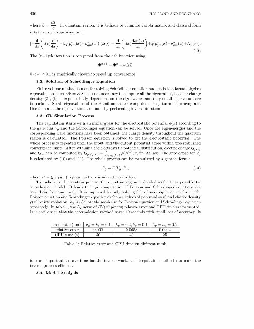
semiclassical model. It leads to large computation if Poisson and Schrodinger equations aresolved on the same mesh. It is improved by only solving Schrodinger equation on fine mesh.Poisson equation and Schrodinger equation exchange values of potential ψ(x) and charge densityρ(x) by interpolation. hp, hs denote the mesh size for Poisson equation and Schrodinger equationseparately. In table 1, the L2 norm of CV(40 points) relative error and CPU time are presented.It is easily seen that the interpolation method saves 10 seconds with small lost of accuracy. It
mesh size (nm) hp = hs = 0.1 hp = 0.2, hs = 0.1 hp = hs = 0.2relative error 0.002 0.0053 0.0094CPU time (s) 50 40 25
Table 1: Relative error and CPU time on different mesh
is more important to save time for the inverse work, so interpolation method can make theinverse process efficient.
3.4. Model Analysis
Model Analysis and Parameter Extraction For MOS Capacitor Including Quantum Mechanical Effects 407
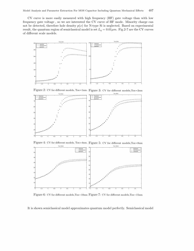
CV curve is more easily measured with high frequency (HF) gate voltage than with lowfrequency gate voltage , so we are interested the CV curve of HF mode. Minority charge cannot be detected, therefore hole density p(x) for N-type Si is neglected. Based on experimentalresult, the quantum region of semiclassical model is set Lq = 0.01µm. Fig.2-7 are the CV curvesof different scale models.
−2 −1.5 −1 −0.5 0 0.5 1 1.5 20
50
100
150
200
250
300Tox=1nm
classicalsemiclassicalquantum
Figure 2: CV for different models, Tox=1nm.
−2 −1.5 −1 −0.5 0 0.5 1 1.5 20
50
100
150Tox=2nm
classicalsemiclassicalquantum
Figure 3: CV for different models,Tox=2nm
−2 −1.5 −1 −0.5 0 0.5 1 1.5 210
20
30
40
50
60
70
80Tox=4nm
ClassicalSemiclassicalQuantum
Figure 4: CV for different models, Tox=4nm.
−2 −1.5 −1 −0.5 0 0.5 1 1.5 210
15
20
25
30
35
40
45Tox=8nm
ClassicalSemiclassicalQuantum
Figure 5: CV for different models,Tox=8nm
−2 −1.5 −1 −0.5 0 0.5 1 1.5 25
10
15
20
25
30
35
40
45Tox=10nm
classicalsemiclassicalquantum
Figure 6: CV for different models,Tox=10nm
−2 −1.5 −1 −0.5 0 0.5 1 1.5 212
14
16
18
20
22
24
26
28
30Tox=15nm
QuantumSemiclassicalClassical
Figure 7: CV for different models,Tox=15nm
It is shown semiclassical model approximates quantum model perfectly. Semiclassical model
408 H.Y. JIAND AND P.W. ZHANG
and quantum model are approaching classical model as oxide layer increases. To compute 40CV points, semiclassical model consumes about 40 seconds while it takes quantum model nearlyhalf hour. Semiclassical model not only saves the computing time greatly, but also includesQM effects correctly, so it is a good model to do the inverse work.
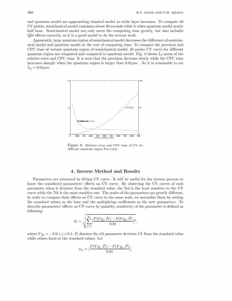
Apparently, large quantum region of semiclassical model decreases the difference of semiclas-sical model and quantum model at the cost of computing time. To compare the precision andCPU time of variant quantum region of semiclassical model, 40 points CV curve for differentquantum region are computed and compared to quantum model. Fig. 8 shows L2 norm of therelative error and CPU time. It is seen that the precision decrease slowly while the CPU timeincreases sharply when the quantum region is larger than 0.01µm . So it is reasonable to setLq = 0.01µm.
0 0.005 0.01 0.015 0.02 0.025 0.03 0.035 0.04 0.045 0.050
0.2
0.4
CPU time(s)
CV relative errorCV relative error L2 normCV relative error
thickness of quantum region 0 0.005 0.01 0.015 0.02 0.025 0.03 0.035 0.04 0.045 0.05
0
500
1000
Figure 8: Relative error and CPU time of CV fordifferent quantum region.Tox=1nm
4. Inverse Method and Results
Parameters are extracted by fitting CV curve. It will be useful for the inverse process toknow the considered parameters’ effects on CV curve. By observing the CV curves of eachparameter when it deviates from the standard value, the 3rd is the least sensitive to the CVcurve while the 7th is the most sensitive one. The scales of the parameters are greatly different.In order to compare their effects on CV curve in the same scale, we normalize them by settingthe standard values as the base and the multiplying coefficients as the new parameters. Todescribe parameters’ effects on CV curve by quantity, sensitivity of the parameter is defined asfollowing:
Si =
√
√
√
√
41∑
j=1
[F (V gj , Pi) − F (V gj, P )
0.01]2,
where V gj = −2.0+ j× 0.1, Pi denotes the ith parameter deviates 1% from the standard valuewhile others fixed at the standard values. Let
aij = [F (V gj , Pi) − F (V gj , P )
0.01],
Model Analysis and Parameter Extraction For MOS Capacitor Including Quantum Mechanical Effects 409
where A = (aij)8×41,M = AA′ and A′ is the transfer matrix of A. Condition number of matrixM reflects the property of the inverse problem. Here the condition number (CN) of M andsensitivity of the parameters are presented in Table 2: It is obvious that P3(Nconst) is the least
S1 S2 S3 S4 S5
0.1548 0.1355 0.0106 0.5065 0.9910S6 S7 S8 CN
0.0467 3.8880 0.4066 1.8717× 10¹²
Table 2: Parameter sensitivities in semiclassical model of HF mode
sensitive parameter. It may cause much trouble in inverse process. CN of HF model reaches1012 which may cause much difficulty to extract the parameters simultaneously. Some techniqueis needed to do the inverse work.
For a group {Cgi}n
i=1 measured at {Vgi}n
i=1 correspondingly, the inverse problem is to confirmP which minimize the difference of {Cgi
}ni=1 to {F (Vgi
, P )}ni=1 at some sense. It is convenient
to use L2 norm for the fitting problem. If the Newton method is used to solve the least squareproblem directly, the large condition number 1012 of Jacobi matrix undoubtedly makes the in-verse problem ill-conditioned. Here we implement the Levenberg-Marquardt (LM) optimizationmethod to overcome this trouble. The object function is:
G(P ) =
n∑
i=1
[Cgi
− F (Vgi, P )
Cgi
]2 + β||P ||2.
Newton method is used to determine P to minimize G(P ) as β → 0. The total error is set tobe :
E(P ) =
n∑
i=1
[Cgi
− F (Vgi, P )
Cgi
]2.
Table 3 gives the considered parameters’ standard values as the exact values and deviate up10% as the initial values for numerical simulation. In Table 4, the inverse results are presentedwhen parameters are extracted simultaneously.
parameter P1 P2 P3 P4
exact value 1.0 0.002 0.1 5.0initial value 1.1 0.0022 0.11 5.5parameter P5 P6 P7 P8
exact value 0.0 0.1 0.0025 0.15initial value 0.1 0.11 0.00275 0.0165
Table 3: The standard values and the initial values
The inverse results verify the correctness of the prediction by the CN analysis. The 3rdparameter Nconst can not come back to its standard value. We should add some technique tothe inverse process. From the sensitivity analysis, the 3rd parameter is the least sensitive one.Our idea is to freeze the 3rd one firstly. After extracting the other parameters to some extent,put the 3rd into the inverse process. This method improves the precision of the inverse resultgreatly. In table 5, the inverse results with this technique are presented.
410 H.Y. JIAND AND P.W. ZHANG
parameter P1 P2 P3 P4
inverse value 0.99811438 0.00199548 0.14281769 4.95687738relative error 0.00188562 0.00226 0.4281769 0.00862456parameter P5 P6 P7 P8
inverse value 0.00005649 0.09944950 0.00250001 0.14999929relative error 0.00005649 0.005505 0.000004 0.000007
Table 4: Inverse results for semiclassical model of HF mode
parameter P1 P2 P3 P4
inverse value 1.00025734 0.00200062 0.10855365 4.99036102relative error 0.00025734 0.00031 0.0855365 0.0019278parameter P5 P6 P7 P8
inverse value 0.00001437 0.09987529 0.0025000 0.14999860relative error 0.00001437 0.0012471 0.000000 0.000009
Table 5: Inverse results with order technique
We did a lot of inverse experiments with different initial cases. If the initial values deviatenot more than 20%, the inverse result is satisfied. It is acceptable for practical device design.
5. Conclusion
This paper mainly analyzes different scale models of 1-D MOS capacitor. Numerical resultsshow that semiclassical model includes QM effect as exactly as quantum model. Semiclassicalmodel is not time-consuming, so it is a good choice to do parameters extraction for ultrathinoxide device. With semiclassical model, the parameters’ effects to the CV curve is firstlyconsidered. It is very helpful for us to propose an efficient inverse strategy. When the initialvalues offset is less than 20%, our strategy can give good inverse results. By a measured CVcurve, we can use simplified model to give a guess value for sensitive parameters which differsnot more than 20% from the exact value. So our strategy is applicable for practical problem.
As the thickness of the oxide layer decreases to sub-2.0nm, the tunnelling current increasesin a nearly exponential manner. This increase in current adversely affects the MOS deviceperformance [3, 10]. Thus, it is important to predict the tunnelling current for the developmentof advanced MOS device. The device decreases equally in each dimension, 2-D model must beconsidered for smaller dimension device. We will consider these in future work.Acknowledgement. The authors are very grateful to Professors Wei Cai and Xiaoyang Liufor their helpful discussions.
References
[1] N. Arora, MOSFET models for VLSI circuit simulation, theory and practice, Wien: Springer–
Verlag, 1993.
[2] Technology roadmap for semiconductors, Semiconductor Industry Assoc., Austin, Tx, 1997.
[3] Chang-Hoon Choi, Jung-Suk Goo, Tae-Young Oh and Zhiping Yu, MOS C-V characterization of
ultrathin gate oxide thickness (1.3-1.8nm), IEEE Electron Device Letters, 20 (1999), 292-294.
[4] J.H. Davies, The physics of low-dimensional semiconductors, an introduction, Cambridge Univer-
sity Press Oxford, 1998.
Model Analysis and Parameter Extraction For MOS Capacitor Including Quantum Mechanical Effects 411
[5] S.A. Harelard, S. Jallepalli and G. Chindalore, A simple model for quantum mechanical effects
in hole inversion layers in silicon PMOS device, IEEE Transactions on electron device, 44 (1997),
1172-1173.
[6] K. Iniewski and C.A.T. Salama , A new approach to CV profiling with sub-Debye-length resolution,
Solid-st. Electron, 34 (1991), 309-314.
[7] F. Rana, S. Tiwari and D.A. Buchanan, Self-consistent modeling of accumulation layers and tun-
nelling currents through very thin oxides, Appl. Phys. Lett., 69 (1996), 1104-1106.
[8] Qiqing Shu, Theory of electron tunelling, Senscice Publisher, 1998.
[9] J. Sune, P. Olivo and B. Rcco, Self-consistent solution of the Poisson and Schrdinger equations in
accumulated semiconductor-insulator interfaces, J. Appl. Phys., 70 (1991), 337-345.
[10] Nian Yang, W.K. Henson, and J. R. Hauser, Modeling study of ultrathin gate tunnelling current
and capacitance-voltage measurments in MOS device, IEEE Transactions on electron Device, 46
(1979), 1464-1471.
[11] T. Yu and W. Cai, FIFA Fast interpolation and filtering algorithm for calculating dyadic Green’s
function in the electromagnetic scattering of multi-layered structures, Commun. Comput. Phys.,
1 (2006), 229-260.
[12] Pingwen Zhang, Yi Sun, Haiyan Jiang and Wei Yao, Multi-scale methods for inverse modeling in
1-D MOS capacitor, Journal of Computational Mathematics, 21 (2003), 85-100.