MAX3949 11.3Gps Lo-Poer AC-Cople Laser Drier · PDF fileand the laser modulator can be...
38
General Description The MAX3949 is a 3.3V, multirate, low-power laser diode driver designed for Ethernet, Fibre Channel, and SONET transmission systems at data rates up to 11.3Gbps. This device is optimized to drive a differential transmit- ter optical subassembly (TOSA) with a 25Ω flex circuit. The unique design of the output stage enables use of unmatched TOSAs. The device receives differential AC-coupled signals with on-chip termination. It can deliver laser modulation cur- rents of up to 85mA at an edge speed of 22ps (20% to 80%) into a 5Ω external differential load. The device is designed to have a high-bandwidth differential signal path with on-chip back termination resistors integrated into its outputs. An input equalization block can be activated to compensate for SFP+ host connector losses. The inte- grated bias circuit provides programmable laser bias cur- rents up to 105mA. Both the laser bias current generator and the laser modulator can be disabled from a single pin. The use of a 3-wire digital interface reduces the pin count while permitting adjustment of input equalization, polar- ity, output deemphasis, and modulation and bias currents without the need for external components. The device is available in a 3mm x 3mm, 16-pin TQFN package, and is specified for the -40°C to +95°C extended temperature range. Benefits and Features ● Low Power Consumption ● Saves Board Space • Small 3mm x 3mm Package ● Flexibility • Programmable Modulation Current Up to 85mA (5Ω Load) • Programmable Bias Current Up to 105mA • Programmable Input Equalization and Output Deemphasis ● Safety • Supports SFF-8431 SFP+ MSA and SFF-8472 Digital Diagnostic • Integrated Eye Safety Features with Maskable Faults • Bias Current Monitor Applications ● 10GBASE-LR SFP+ Optical Transceivers ● 10GBASE-LRM SFP+ Optical Transceivers ● OC192-SR SFP+ SDH/SONET Transceivers Ordering Information appears at end of data sheet. 19-6317; Rev 1; 4/14 MAX3949 11.3Gbps, Low-Power, AC-Coupled Laser Driver EVALUATION KIT AVAILABLE
Transcript of MAX3949 11.3Gps Lo-Poer AC-Cople Laser Drier · PDF fileand the laser modulator can be...
General DescriptionThe MAX3949 is a 3.3V, multirate, low-power laser diode driver designed for Ethernet, Fibre Channel, and SONET transmission systems at data rates up to 11.3Gbps. This device is optimized to drive a differential transmit-ter optical subassembly (TOSA) with a 25Ω flex circuit. The unique design of the output stage enables use of unmatched TOSAs.The device receives differential AC-coupled signals with on-chip termination. It can deliver laser modulation cur-rents of up to 85mA at an edge speed of 22ps (20% to 80%) into a 5Ω external differential load. The device is designed to have a high-bandwidth differential signal path with on-chip back termination resistors integrated into its outputs. An input equalization block can be activated to compensate for SFP+ host connector losses. The inte-grated bias circuit provides programmable laser bias cur-rents up to 105mA. Both the laser bias current generator and the laser modulator can be disabled from a single pin.The use of a 3-wire digital interface reduces the pin count while permitting adjustment of input equalization, polar-ity, output deemphasis, and modulation and bias currents without the need for external components. The device is available in a 3mm x 3mm, 16-pin TQFN package, and is specified for the -40°C to +95°C extended temperature range.
Benefits and Features Low Power Consumption Saves Board Space
• Small 3mm x 3mm Package Flexibility
• Programmable Modulation Current Up to 85mA (5Ω Load)
• Programmable Bias Current Up to 105mA• Programmable Input Equalization and Output
Deemphasis Safety
• Supports SFF-8431 SFP+ MSA and SFF-8472 Digital Diagnostic
• Integrated Eye Safety Features with Maskable Faults
• Bias Current Monitor
Applications 10GBASE-LR SFP+ Optical Transceivers 10GBASE-LRM SFP+ Optical Transceivers OC192-SR SFP+ SDH/SONET Transceivers
Ordering Information appears at end of data sheet.
19-6317; Rev 1; 4/14
MAX3949 11.3Gbps, Low-Power, AC-Coupled Laser Driver
EVALUATION KIT AVAILABLE
VCC, VCCT............................................................-0.3V to +4.0V|VCC - VCCT| .................................................................... < 0.5VVoltage Range at TIN+, TIN-, DISABLE,
SDA, SCL, CSEL, VSEL, FAULT, and BMON .... -0.3V to VCCVoltage Range at
TOUT-, TOUT+ ......................(VCCT - 1.3V) to (VCCT + 1.3V)Current Range into TIN+ and TIN- ................... -20mA to +20mACurrent Range into BIAS ................................... 0mA to +120mA
Voltage Range at BIAS ........................................... 0.4V to 2.5VCurrent into TOUT+ and TOUT- .....................................+150mAContinuous Power Dissipation (TA = +70°C) TQFN (derate 20.8mW/°C above +70°C)...............1666.7mWStorage Temperature Range ............................ -55°C to +150°CDie Attach Temperature ...................................................+400°CLead Temperature (soldering, 10s) .................................+300°CSoldering Temperature (reflow) .......................................+260°C
PACKAGE TYPE: 16-PIN TQFNPackage Code T1633+5Outline Number 21-0136Land Pattern Number 90-0032THERMAL RESISTANCE, FOUR-LAYER BOARDJunction to Ambient (θJA) 48°C/WJunction to Case (θJC) 10°C/W
MAX3949 11.3Gbps, Low-Power, AC-Coupled Laser Driver
www.maximintegrated.com Maxim Integrated 2
Package thermal resistances were obtained using the method described in JEDEC specification JESD51-7, using a four-layer board. For detailed information on package thermal considerations, refer to www.maximintegrated.com/thermal-tutorial.
Absolute Maximum Ratings
Stresses beyond those listed under “Absolute Maximum Ratings” may cause permanent damage to the device. These are stress ratings only, and functional operation of the device at these or any other conditions beyond those indicated in the operational sections of the specifications is not implied. Exposure to absolute maximum rating conditions for extended periods may affect device reliability.
Package Information
For the latest package outline information and land patterns (footprints), go to www.maximintegrated.com/packages. Note that a “+”, “#”, or “-” in the package code indicates RoHS status only. Package drawings may show a different suffix character, but the drawing pertains to the package regardless of RoHS status.
(VCC = VCCT = 2.95V to 3.63V, TA = -40°C to +95°C; typical values are at VCC = VCCT = 3.3V, TA = +25°C, IBIAS = 60mA, LDMOD = 40mA, and 14Ω single-ended electrical output load, unless otherwise noted. See AC Test Setup for electrical setup.) (Note 1)
PARAMETER SYMBOL CONDITIONS MIN TYP MAX UNITS
POWER SUPPLY
Power-Supply Current ICCExcludes output current through the external pullup inductors (Note 2) 55 70 mA
Power-Supply Voltage VCCT, VCC 2.95 3.63 V
POWER-ON RESET
VCC for Enable High 2.55 2.75 V
VCC for Enable Low 2.3 2.45 V
DATA INPUT SPECIFICATION
Input Data Rate 1 10.3 11.3 Gbps
Differential Input Voltage VIN
Launch amplitude into FR4 transmission line ≤ 12in, SET_TXEQ[1:0] = 01b, SET_TXEQ[1:0] = 11b
0.2 0.8
VP-PSET_TXEQ[1:0] = 01b, SET_TXEQ[1:0] = 11b, outside of optimized range
0.15 1.0
SET_TXEQ[1:0] = 00b 0.15 1.0
Common-Mode Input Voltage VCM 2.15 V
Differential Input Resistance RIN 75 100 125 Ω
Differential Input S-Parameters (Note 3)
SCD11 0.1GHz ≤ f ≤ 11.3GHz -30
dBSDD11f ≤ 4.1GHz -19
4.1GHz ≤ f ≤ 11.3GHz -16
SCC11 1GHz ≤ f ≤ 11.3GHz, ZCM_SOURCE = 25Ω -13
BIAS CURRENT GENERATOR (Figure 3)
Maximum BIAS DAC Current IBIASMAX Current into BIAS pin 85 105 mA
Minimum BIAS DAC Current IBIASMIN Current into BIAS pin 5 mA
BIAS-Off Current IBIAS-OFF 0.1 mA
BIAS DAC LSB Size 200 µA
BIAS DAC Integral Nonlinearity INL 5mA ≤ IBIAS ≤ 85mA ±0.5 %FS
BIAS DAC Differential Nonlinearity DNL Guaranteed monotonic at 8-bit resolution,
SET_IBIAS[8:1] ±0.5 LSB
BIAS Current DAC Stability 5mA ≤ IBIAS ≤ 85mA, VBIAS = 1.5V (Notes 4, 5) 1 4 %
BIAS Compliance Voltage 0.9 1.5 2.1 V
MAX3949 11.3Gbps, Low-Power, AC-Coupled Laser Driver
www.maximintegrated.com Maxim Integrated 3
Electrical Characteristics
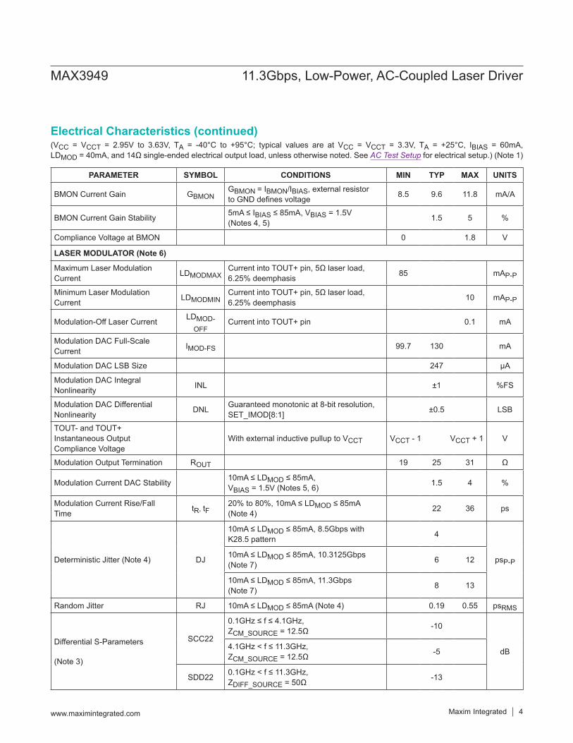
(VCC = VCCT = 2.95V to 3.63V, TA = -40°C to +95°C; typical values are at VCC = VCCT = 3.3V, TA = +25°C, IBIAS = 60mA, LDMOD = 40mA, and 14Ω single-ended electrical output load, unless otherwise noted. See AC Test Setup for electrical setup.) (Note 1)
PARAMETER SYMBOL CONDITIONS MIN TYP MAX UNITS
BMON Current Gain GBMONGBMON = IBMON/IBIAS, external resistor to GND defines voltage 8.5 9.6 11.8 mA/A
BMON Current Gain Stability 5mA ≤ IBIAS ≤ 85mA, VBIAS = 1.5V (Notes 4, 5) 1.5 5 %
Compliance Voltage at BMON 0 1.8 V
LASER MODULATOR (Note 6)
Maximum Laser Modulation Current LDMODMAX
Current into TOUT+ pin, 5Ω laser load, 6.25% deemphasis 85 mAP-P
Minimum Laser Modulation Current LDMODMIN
Current into TOUT+ pin, 5Ω laser load, 6.25% deemphasis 10 mAP-P
Modulation-Off Laser Current LDMOD-OFF
Current into TOUT+ pin 0.1 mA
Modulation DAC Full-Scale Current IMOD-FS 99.7 130 mA
Modulation DAC LSB Size 247 µA
Modulation DAC Integral Nonlinearity INL ±1 %FS
Modulation DAC Differential Nonlinearity DNL Guaranteed monotonic at 8-bit resolution,
SET_IMOD[8:1] ±0.5 LSB
TOUT- and TOUT+ Instantaneous Output Compliance Voltage
With external inductive pullup to VCCT VCCT - 1 VCCT + 1 V
Modulation Output Termination ROUT 19 25 31 Ω
Modulation Current DAC Stability 10mA ≤ LDMOD ≤ 85mA, VBIAS = 1.5V (Notes 5, 6) 1.5 4 %
Modulation Current Rise/Fall Time tR, tF
20% to 80%, 10mA ≤ LDMOD ≤ 85mA (Note 4) 22 36 ps
Deterministic Jitter (Note 4) DJ
10mA ≤ LDMOD ≤ 85mA, 8.5Gbps with K28.5 pattern 4
psP-P10mA ≤ LDMOD ≤ 85mA, 10.3125Gbps (Note 7) 6 12
10mA ≤ LDMOD ≤ 85mA, 11.3Gbps (Note 7) 8 13
Random Jitter RJ 10mA ≤ LDMOD ≤ 85mA (Note 4) 0.19 0.55 psRMS
Differential S-Parameters
(Note 3)
SCC22
0.1GHz ≤ f ≤ 4.1GHz, ZCM_SOURCE = 12.5Ω -10
dB4.1GHz < f ≤ 11.3GHz, ZCM_SOURCE = 12.5Ω -5
SDD22 0.1GHz < f ≤ 11.3GHz, ZDIFF_SOURCE = 50Ω -13
MAX3949 11.3Gbps, Low-Power, AC-Coupled Laser Driver
www.maximintegrated.com Maxim Integrated 4
Electrical Characteristics (continued)
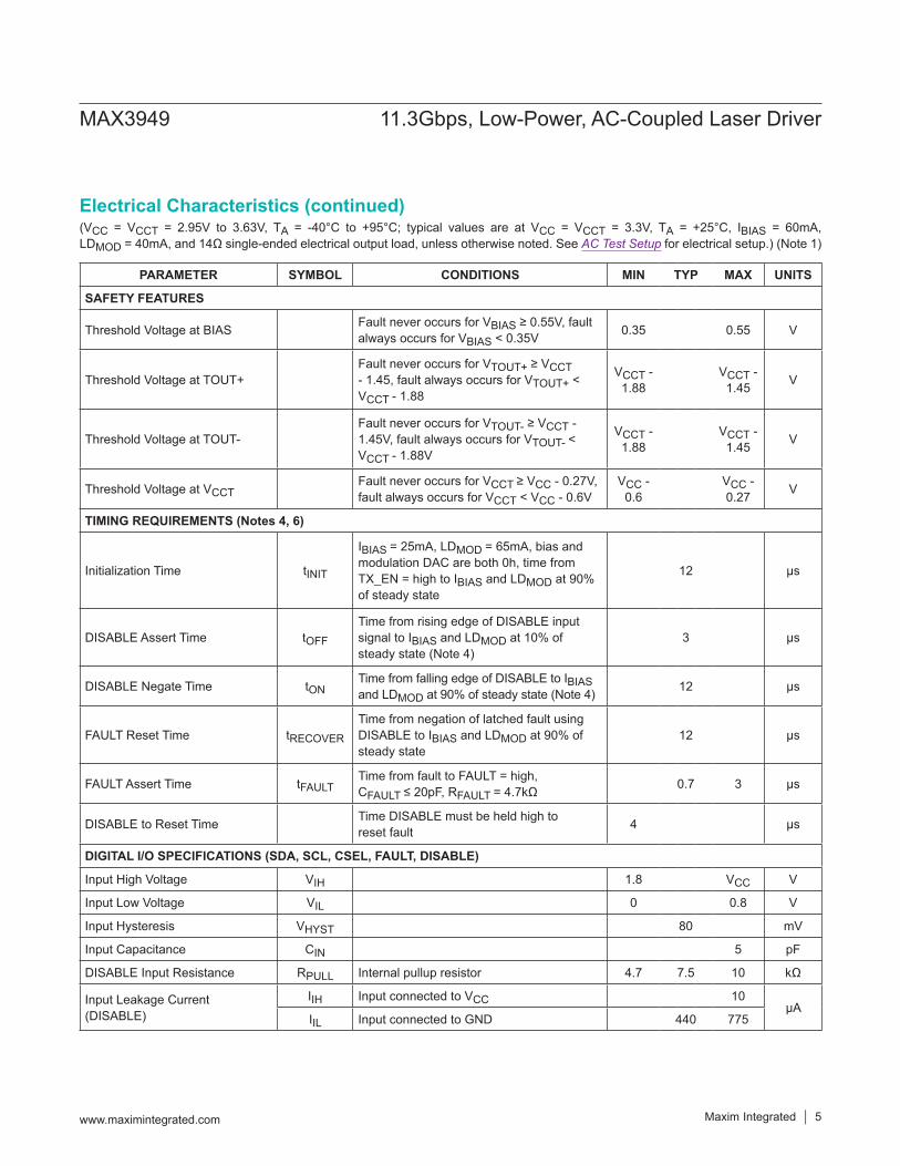
(VCC = VCCT = 2.95V to 3.63V, TA = -40°C to +95°C; typical values are at VCC = VCCT = 3.3V, TA = +25°C, IBIAS = 60mA, LDMOD = 40mA, and 14Ω single-ended electrical output load, unless otherwise noted. See AC Test Setup for electrical setup.) (Note 1)
PARAMETER SYMBOL CONDITIONS MIN TYP MAX UNITS
SAFETY FEATURES
Threshold Voltage at BIAS Fault never occurs for VBIAS ≥ 0.55V, fault always occurs for VBIAS < 0.35V 0.35 0.55 V
Threshold Voltage at TOUT+Fault never occurs for VTOUT+ ≥ VCCT - 1.45, fault always occurs for VTOUT+ < VCCT - 1.88
VCCT - 1.88
VCCT - 1.45 V
Threshold Voltage at TOUT-Fault never occurs for VTOUT- ≥ VCCT - 1.45V, fault always occurs for VTOUT- < VCCT - 1.88V
VCCT - 1.88
VCCT - 1.45 V
Threshold Voltage at VCCTFault never occurs for VCCT ≥ VCC - 0.27V, fault always occurs for VCCT < VCC - 0.6V
VCC - 0.6
VCC - 0.27 V
TIMING REQUIREMENTS (Notes 4, 6)
Initialization Time tINIT
IBIAS = 25mA, LDMOD = 65mA, bias and modulation DAC are both 0h, time from TX_EN = high to IBIAS and LDMOD at 90% of steady state
12 µs
DISABLE Assert Time tOFF
Time from rising edge of DISABLE input signal to IBIAS and LDMOD at 10% of steady state (Note 4)
3 µs
DISABLE Negate Time tONTime from falling edge of DISABLE to IBIAS and LDMOD at 90% of steady state (Note 4) 12 µs
FAULT Reset Time tRECOVER
Time from negation of latched fault using DISABLE to IBIAS and LDMOD at 90% of steady state
12 µs
FAULT Assert Time tFAULTTime from fault to FAULT = high, CFAULT ≤ 20pF, RFAULT = 4.7kΩ 0.7 3 µs
DISABLE to Reset Time Time DISABLE must be held high to reset fault 4 µs
DIGITAL I/O SPECIFICATIONS (SDA, SCL, CSEL, FAULT, DISABLE)
Input High Voltage VIH 1.8 VCC V
Input Low Voltage VIL 0 0.8 V
Input Hysteresis VHYST 80 mV
Input Capacitance CIN 5 pF
DISABLE Input Resistance RPULL Internal pullup resistor 4.7 7.5 10 kΩ
Input Leakage Current (DISABLE)
IIH Input connected to VCC 10µA
IIL Input connected to GND 440 775
MAX3949 11.3Gbps, Low-Power, AC-Coupled Laser Driver
www.maximintegrated.com Maxim Integrated 5
Electrical Characteristics (continued)
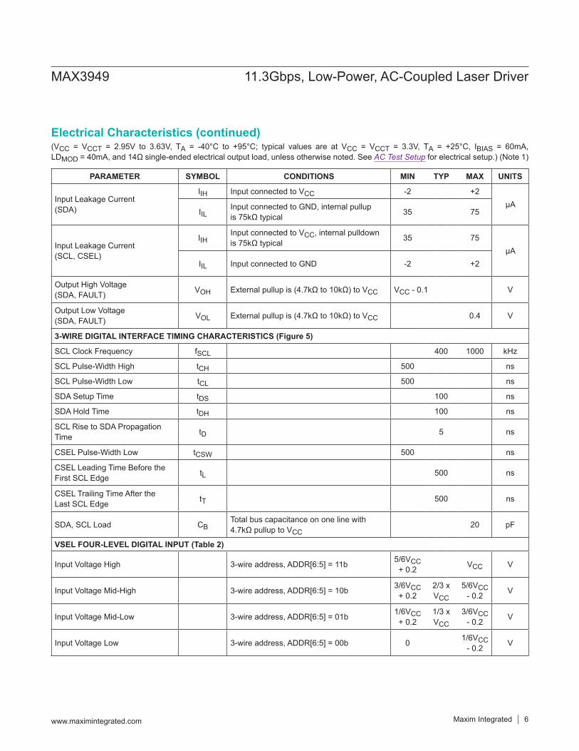
(VCC = VCCT = 2.95V to 3.63V, TA = -40°C to +95°C; typical values are at VCC = VCCT = 3.3V, TA = +25°C, IBIAS = 60mA, LDMOD = 40mA, and 14Ω single-ended electrical output load, unless otherwise noted. See AC Test Setup for electrical setup.) (Note 1)
PARAMETER SYMBOL CONDITIONS MIN TYP MAX UNITS
Input Leakage Current (SDA)
IIH Input connected to VCC -2 +2µA
IILInput connected to GND, internal pullup is 75kΩ typical 35 75
Input Leakage Current (SCL, CSEL)
IIHInput connected to VCC, internal pulldown is 75kΩ typical 35 75
µAIIL Input connected to GND -2 +2
Output High Voltage (SDA, FAULT) VOH External pullup is (4.7kΩ to 10kΩ) to VCC VCC - 0.1 V
Output Low Voltage (SDA, FAULT) VOL External pullup is (4.7kΩ to 10kΩ) to VCC 0.4 V
3-WIRE DIGITAL INTERFACE TIMING CHARACTERISTICS (Figure 5)
SCL Clock Frequency fSCL 400 1000 kHz
SCL Pulse-Width High tCH 500 ns
SCL Pulse-Width Low tCL 500 ns
SDA Setup Time tDS 100 ns
SDA Hold Time tDH 100 ns
SCL Rise to SDA Propagation Time tD 5 ns
CSEL Pulse-Width Low tCSW 500 ns
CSEL Leading Time Before the First SCL Edge tL 500 ns
CSEL Trailing Time After the Last SCL Edge tT 500 ns
SDA, SCL Load CBTotal bus capacitance on one line with 4.7kΩ pullup to VCC
20 pF
VSEL FOUR-LEVEL DIGITAL INPUT (Table 2)
Input Voltage High 3-wire address, ADDR[6:5] = 11b 5/6VCC + 0.2 VCC V
Input Voltage Mid-High 3-wire address, ADDR[6:5] = 10b 3/6VCC + 0.2
2/3 x VCC
5/6VCC - 0.2 V
Input Voltage Mid-Low 3-wire address, ADDR[6:5] = 01b 1/6VCC + 0.2
1/3 x VCC
3/6VCC - 0.2 V
Input Voltage Low 3-wire address, ADDR[6:5] = 00b 0 1/6VCC - 0.2 V
MAX3949 11.3Gbps, Low-Power, AC-Coupled Laser Driver
www.maximintegrated.com Maxim Integrated 6
Electrical Characteristics (continued)

(VCC = VCCT = 2.95V to 3.63V, TA = -40°C to +95°C; typical values are at VCC = VCCT = 3.3V, TA = +25°C, IBIAS = 60mA, LDMOD = 40mA, and 14Ω single-ended electrical output load, unless otherwise noted. See AC Test Setup for electrical setup.) (Note 1)
Note 1: Specifications at TA = -40°C and +95°C are guaranteed by design and characterization.Note 2: BIAS is connected to 1.9V. TOUT- and TOUT+ are connected to VCCT through pullup inductors.Note 3: Measured with Agilent 8720ES + ATN-U112A and series RC (39Ω and 0.3pF) between TOUT+ and TOUT- (AC Test
Setup). Note 4: Guaranteed by design and characterization.Note 5: Stability is defined as [(IMEASURED) - (IREFERENCE)]/(IREFERENCE) over the listed current/temperature range and
VCCT = VCC = VCCREF ±5%, VCCREF = 3.3V. Reference current measured at VCCREF and TREF = +25°C.Note 6: LDMOD = IMOD x (1 - DE) x 50/(50 + R), where LDMOD is the effective laser modulation current, IMOD is the modulation
DAC current, DE is the deemphasis percentage, and R is the differential laser load resistance. Example: For RΩ = 5 and DE = 6.25%, LDMOD = 0.852 x IMOD.
Note 7: Equivalent 223 - 1 PRBS pattern = 27 - 1 PRBS + 72 zeros + 27 - 1 PRBS + 72 ones.
MAX3949 11.3Gbps, Low-Power, AC-Coupled Laser Driver
www.maximintegrated.com Maxim Integrated 7
Electrical Characteristics (continued)
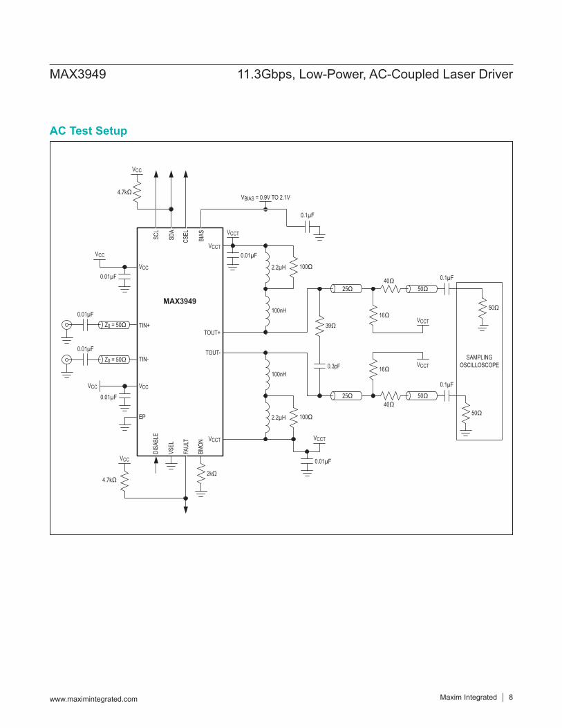
AC Test Setup
MAX3949 11.3Gbps, Low-Power, AC-Coupled Laser Driver
www.maximintegrated.com Maxim Integrated 8
0.01µF
SCL
SDA
CSEL
BIAS
0.01µFTIN+
TOUT+
TOUT-
VCCT
TIN-
4.7kΩ
0.01µF
VCCVCCT
EP
DISA
BLE
FAUL
T
BMON
VCC
VCC
VCC
VCCT
VBIAS = 0.9V TO 2.1V
VCCT
VCC
VCCT
VCC
Z0 = 50Ω
4.7kΩ2kΩ
0.01µFZ0 = 50Ω
0.1µF
0.01µF
100nH
40Ω
40Ω
16Ω
25Ω
25Ω
50Ω
50Ω
0.1µF
SAMPLINGOSCILLOSCOPE
0.1µF
50Ω
50Ω
VCCT
16Ω
100Ω
39Ω
VSEL
0.01µF
0.3pF
MAX3949
100nH
2.2µH
100Ω2.2µH
(Typical values are at VCC = VCCT = 3.3V, TA = +25°C, data pattern = 27 - 1 PRBS + 72 zeros + 27 - 1 PRBS (inverted) + 72 ones, unless otherwise noted.)
MAX3949 11.3Gbps, Low-Power, AC-Coupled Laser Driver
Maxim Integrated 9www.maximintegrated.com
Typical Operating Characteristics
10.3Gbps OPTICAL EYE DIAGRAMMAX3949 toc01
16ps/div
FREQUENCY (Hz)
SCC1
1 (dB
)
10G1G100M 100G
INPUT COMMON-MODE RETURN LOSSvs. FREQUENCY
MAX
3949
toc0
4
-25
-20
-15
-10
-5
0
-30
OUTPUT COMMMON-MODE RETURN LOSSvs. FREQUENCY
MAX
3949
toc0
7
FREQUENCY (Hz)
SCC2
2 (dB
)
10G1G
-30
-25
-20
-15
-10
-5
0
-35100M 100G
10Gbps ELECTRICAL EYE DIAGRAMMAX3949 toc02
20ps/div
FREQUENCY (Hz)
SCD1
1 (dB
)
10G1G100M 100G
INPUT DIFFERENTIAL TO COMMON-MODERETURN LOSS vs. FREQUENCY
MAX
3949
toc0
5
-50
-40
-30
-20
-10
0
-60
RANDOM JITTER vs. MODULATIONCURRENT (AT LOAD)
MAX
3949
toc0
8
MODULATION CURRENT (mAP-P)
RJ (p
s RMS
)
807050 6020 30 4010
0.1
0.2
0.3
0.4
0.5
0.6
0.7
11.3Gbps, 1111 0000 PATTERN
0.8
0.9
1.0
00 90
FREQUENCY (Hz)
SDD1
1 (dB
)
10G1G100M 100G
INPUT DIFFERENTIAL RETURN LOSSvs. FREQUENCY
MAX
3949
toc0
3
-50
-40
-30
-20
-10
0
-60
OUTPUT DIFFERENTIAL RETURN LOSSvs. FREQUENCY
MAX
3949
toc0
6
FREQUENCY (Hz)
SDD2
2 (dB
)
10G1G
-30
-25
-20
-15
-10
-5
0
-35100M 100G
SUPPLY CURRENT vs. TEMPERATURE(IMOD = 40mAP-P, IBIAS = 60mA)
MAX
3949
toc0
9
TEMPERATURE (°C)
SUPP
LY C
URRE
NT (m
A)
9580655035205-10-25
50
60
70
80
40-40
CURRENT INTO VCC AND VCCT PINS EXCLUDING CURRENT THROUGHPULLUP INDUCTORS
(Typical values are at VCC = VCCT = 3.3V, TA = +25°C, data pattern = 27 - 1 PRBS + 72 zeros + 27 - 1 PRBS (inverted) + 72 ones, unless otherwise noted.)
MAX3949 11.3Gbps, Low-Power, AC-Coupled Laser Driver
Maxim Integrated 10www.maximintegrated.com
Typical Operating Characteristics (continued)
TOTAL CURRENT vs. TEMPERATURE(LDMOD AT LOAD = 40mAP-P, IBIAS = 60mA)
MAX
3949
toc1
0
SUPP
LY C
URRE
NT (m
A)
150
160
170
180
190
200
210
220
140
TEMPERATURE (°C)9580655035205-10-25-40
CURRENT INTO VCC AND VCCT PINSPLUS MODULATION AND BIAS CURRENT
25Ω LOAD
5Ω LOAD
MODULATION CURRENT DEEMPHASISvs. MANUAL DEEMPHASIS SETTING
MAX
3949
toc1
3
SET_TXDE[6:0]
DEEM
PHAS
IS (%
)
110907050
1
2
3
4
5
6
7
8
9
030 130
SET_IMOD[8:0] = 354dTXDE_MD[1:0] = 2d
BIAS MONITOR CURRENTvs. TEMPERATURE
MAX
3949
toc1
4
BMON
CUR
RENT
(uA)
TEMPERATURE (°C)9580655035205-10-25-40
100
200
300
400
500
600
700
0
IBIAS = 60mAIBIAS = 30mA
IBIAS = 10mA
EDGE SPEEDvs. MODULATION CURRENT
MAX
3949
toc1
5
IMOD (mA)
EDGE
SPE
ED (p
s)
806020 40
15
20
25
30
40
35
45
50
100 100
10Gbps, 11111 00000 PATTERN20% TO 80%
EDGE SPEEDvs. DEEMPHASIS SETTING
MAX
3949
toc1
6
SET_TXDE[6:0]
EDGE
SPE
ED (p
s)
1109050 70
15
20
25
30
40
35
45
50
1030 130
SET_IMOD[8:0] = 354d20% TO 80%10Gbps, 11111 00000 PATTERN
FALL TIME
RISE TIME
BIAS CURRENT vs. DAC SETTING
MAX
3949
toc1
1
SET_IBIAS[8:0]
BIAS
CUR
RENT
(mA)
500400300200100
20
40
60
80
100
120
00 600
MODULATION CURRENT (AT LOAD)vs. DAC SETTING
MAX
3949
toc1
2
SET_IMOD[8:0]
MODU
LATI
ON C
URRE
NT (m
A P-P
)
500400300200100
10
20
30
40
50
60
70
80
90
100
00 600
25Ω DIFFERENTIAL LOAD
10Ω DIFFERENTIAL LOAD
5Ω DIFFERENTIAL LOAD
(Typical values are at VCC = VCCT = 3.3V, TA = +25°C, data pattern = 27 - 1 PRBS + 72 zeros + 27 - 1 PRBS (inverted) + 72 ones, unless otherwise noted.)
MAX3949 11.3Gbps, Low-Power, AC-Coupled Laser Driver
Maxim Integrated 11www.maximintegrated.com
RESPONSE TO FAULTMAX3949 toc19
2µs/div
EXTERNAL FAULT
HIGHLOW
VOUT
FAULT
DISABLE
OUTPUT
FAULT RECOVERYMAX3949 toc20
4µs/div
EXTERNAL FAULTREMOVED
HIGH
HIGH
LOW
LOW
VOUT
FAULT
DISABLE
OUTPUT
FREQUENT ASSERTION OF DISABLEMAX3949 toc21
4µs/div
EXTERNAL FAULT
HIGH
LOW
LOW
VOUT
FAULT
DISABLE
OUTPUTHIGH
MAX3949 3-WIRE ADDRESSvs. VSEL VOLTAGE
MAX
3949
toc2
2
VSEL
VOL
TAGE
(FRA
CTIO
N OF
VCC
)
VCC/3
2VCC/3
VCC
GNDADDR[6:5] = 00
ADDR[6:5] = 01
ADDR[6:5] = 10
ADDR[6:5] = 11
INDETERMINATE5/6 x VCC±200mV
INDETERMINATE3/6 x VCC ±200mV
INDETERMINATE1/6 x VCC ±200mV
TRANSMITTER DISABLEMAX3949 toc17
1µs/div
3.3V
HIGHLOW
VCC
FAULT
DISABLE
OPTICALOUTPUT
TRANSMITTER ENABLEMAX3949 toc18
4µs/div
3.3V
HIGHLOW
VCC
FAULT
DISABLE
OPTICALOUTPUT
Typical Operating Characteristics (continued)
PIN NAME FUNCTION EQUIVALENT CIRCUIT
1 DISABLE
Disable Input, CMOS. Set to logic-low for normal operation. Logic-high or open disables both the modulation current and the bias current. Internally pulled up by a 7.5kΩ resistor to VCC.
7.5kΩ
VCCVCC
ESDPROTECTION
VCC
DISABLE
2 VSEL
4-Level Input for SPI Device Address Detection. Connecting to VCC sets ADDR[6:5] to 11b, connecting to VCC x 2/3 sets ADDR[6:5] to 10b, connecting to VCC/3 sets ADDR[6:5] to 01b, and connecting to GND sets ADDR[6:5] to 00b.
VSEL
VCC
MAX3949 11.3Gbps, Low-Power, AC-Coupled Laser Driver
www.maximintegrated.com
Pin Description
Pin Configuration
15
16
14
13
5
6
7
FAUL
T
BMON
8
DISA
BLE
CSEL
BIAS
SCL
1 3
TIN+
4
12 10 9
TIN-
EP*
*EXPOSED PAD MUST BE CONNECTED TO GROUND.
VCC
VCCT
TOUT+
TOUT-
VCCTVS
ELSD
A2
11
VCC
TQFN
TOP VIEW
+
MAX3949
PIN NAME FUNCTION EQUIVALENT CIRCUIT
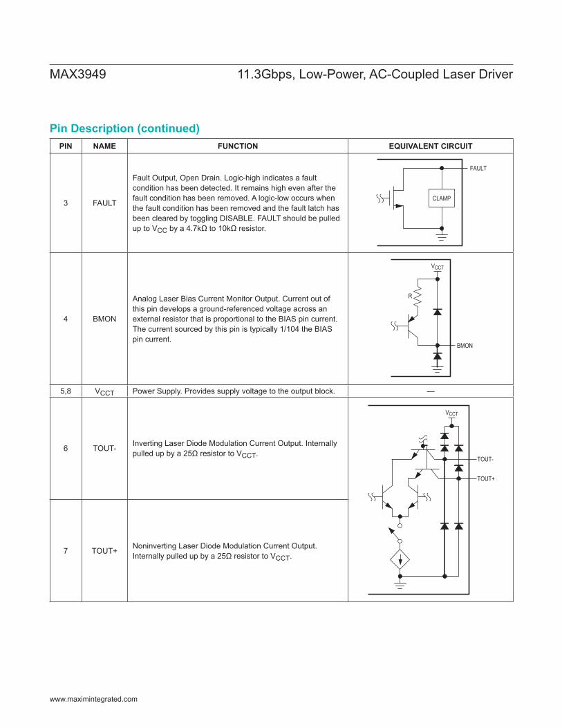
3 FAULT
Fault Output, Open Drain. Logic-high indicates a fault condition has been detected. It remains high even after the fault condition has been removed. A logic-low occurs when the fault condition has been removed and the fault latch has been cleared by toggling DISABLE. FAULT should be pulled up to VCC by a 4.7kΩ to 10kΩ resistor.
FAULT
CLAMP
4 BMON
Analog Laser Bias Current Monitor Output. Current out of this pin develops a ground-referenced voltage across an external resistor that is proportional to the BIAS pin current. The current sourced by this pin is typically 1/104 the BIAS pin current.
BMON
R
VCCT
5,8 VCCT Power Supply. Provides supply voltage to the output block. —
6 TOUT- Inverting Laser Diode Modulation Current Output. Internally pulled up by a 25Ω resistor to VCCT.
VCCT
TOUT-
TOUT+
7 TOUT+ Noninverting Laser Diode Modulation Current Output. Internally pulled up by a 25Ω resistor to VCCT.
MAX3949 11.3Gbps, Low-Power, AC-Coupled Laser Driver
www.maximintegrated.com
Pin Description (continued)
PIN NAME FUNCTION EQUIVALENT CIRCUIT
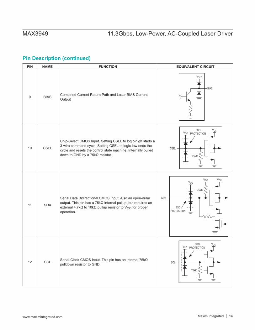
9 BIAS Combined Current Return Path and Laser BIAS Current Output
BIAS
VCCT
10 CSEL
Chip-Select CMOS Input. Setting CSEL to logic-high starts a 3-wire command cycle. Setting CSEL to logic-low ends the cycle and resets the control state machine. Internally pulled down to GND by a 75kΩ resistor. 75kΩ
VCCVCCESD
PROTECTION
CSEL
11 SDA
Serial Data Bidirectional CMOS Input. Also an open-drain output. This pin has a 75kΩ internal pullup, but requires an external 4.7kΩ to 10kΩ pullup resistor to VCC for proper operation.
75kΩ
VCCVCC
ESDPROTECTION
VCC
SDA
12 SCL Serial-Clock CMOS Input. This pin has an internal 75kΩ pulldown resistor to GND.
75kΩ
VCCVCCESD
PROTECTION
SCL
MAX3949 11.3Gbps, Low-Power, AC-Coupled Laser Driver
www.maximintegrated.com Maxim Integrated 14
Pin Description (continued)
PIN NAME FUNCTION EQUIVALENT CIRCUIT
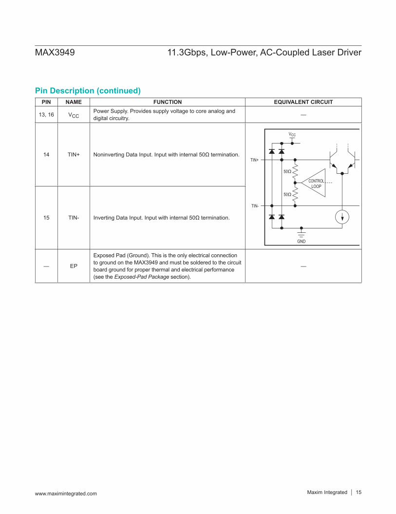
13, 16 VCCPower Supply. Provides supply voltage to core analog and digital circuitry. —
14 TIN+ Noninverting Data Input. Input with internal 50Ω termination.
50Ω
50Ω
VCC
GND
TIN+
TIN-
CONTROLLOOP
15 TIN- Inverting Data Input. Input with internal 50Ω termination.
— EP
Exposed Pad (Ground). This is the only electrical connection to ground on the MAX3949 and must be soldered to the circuit board ground for proper thermal and electrical performance (see the Exposed-Pad Package section).
—
MAX3949 11.3Gbps, Low-Power, AC-Coupled Laser Driver
www.maximintegrated.com Maxim Integrated 15
Pin Description (continued)
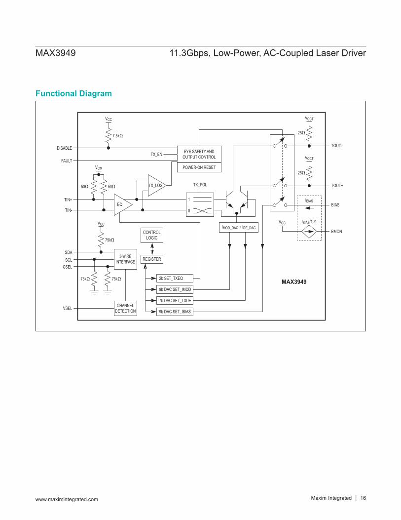
Functional Diagram
MAX3949 11.3Gbps, Low-Power, AC-Coupled Laser Driver
www.maximintegrated.com Maxim Integrated 16
EYE SAFETY ANDOUTPUT CONTROL
TOUT-
TOUT+
BIAS
BMON
TX_EN
TX_POL50Ω50Ω
FAULT
TIN+
TIN-
SDASCL
CSEL
DISABLE
POWER-ON RESET
VCC VCCT
VCCT
7.5kΩ
VCC
VCM
75kΩ
1
0
25Ω
25Ω
EQ
TX_LOS
IMOD_DAC + IDE_DAC
IBIAS
VCC IBIAS/104
VSEL
3-WIREINTERFACE REGISTER
CONTROLLOGIC
CHANNELDETECTION
2b SET_TXEQ
9b DAC SET_IMOD
75kΩ 75kΩ
7b DAC SET_TXDE
9b DAC SET_IBIAS
MAX3949
Detailed DescriptionThe MAX3949 SFP+/QSFP+ laser driver is designed to drive 5Ω to 10Ω TOSAs from 1Gbps to 11.3Gbps. It contains an input buffer with programmable equalization, bias and modulation current DACs, an output driver with adjustable deemphasis, power-on-reset circuitry, bias current monitor, programmable 3-wire address, and eye safety circuitry with maskable fault monitors. A 3-wire digital interface is used to control these functions.
Input Buffer with Programmable EqualizationThe input is internally biased and terminated with 50Ω to a common-mode voltage. The first amplifier stage fea-tures a programmable equalizer for high-frequency losses including a SFP+/QSFP+ host connector. Equalization is controlled by the SET_TXEQ register (Table 1). The TX_POL bit in the TXCTRL register controls the polarity of TOUT- and TOUT+ vs. TIN+ and TIN-. A status indica-tor bit (TXSTAT1 bit 5) monitors the presence of an AC input signal.
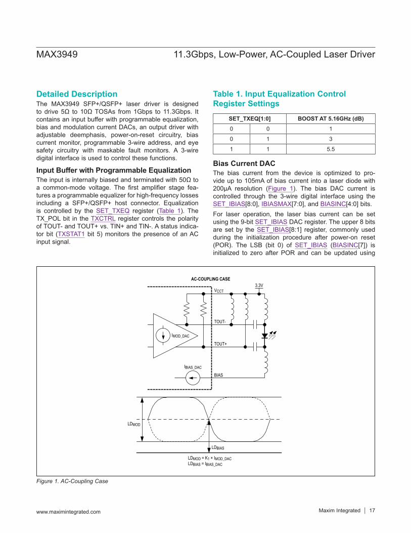
Bias Current DACThe bias current from the device is optimized to pro-vide up to 105mA of bias current into a laser diode with 200µA resolution (Figure 1). The bias DAC current is controlled through the 3-wire digital interface using the SET_IBIAS[8:0], IBIASMAX[7:0], and BIASINC[4:0] bits.For laser operation, the laser bias current can be set using the 9-bit SET_IBIAS DAC register. The upper 8 bits are set by the SET_IBIAS[8:1] register, commonly used during the initialization procedure after power-on reset (POR). The LSB (bit 0) of SET_IBIAS (BIASINC[7]) is initialized to zero after POR and can be updated using
Table 1. Input Equalization Control Register Settings
SET_TXEQ[1:0] BOOST AT 5.16GHz (dB)0 0 1
0 1 3
1 1 5.5
Figure 1. AC-Coupling Case
MAX3949 11.3Gbps, Low-Power, AC-Coupled Laser Driver
www.maximintegrated.com Maxim Integrated 17
AC-COUPLING CASE
VCCT
TOUT-
3.3V
TOUT+
BIAS
IMOD_DAC
IBIAS_DAC
LDMOD
LDBIAS
LDMOD = K1 × IMOD_DACLDBIAS = IBIAS_DAC
the BIASINC register. The IBIASMAX register limits the maximum SET_IBIAS[8:1] DAC code.After initialization the value of the SET_IBIAS DAC register should be updated using the BIASINC register to optimize cycle time and enhance laser safety. The BIASINC register is an 8-bit register. The first 5 bits of BIASINC contain the increment information in two’s com-plement format. Increment values range from -16 to +15 LSBs. If the updated value of SET_IBIAS[8:1] exceeds IBIASMAX[7:0], the IBIASERR warning flag is set and SET_IBIAS[8:1] is set to IBIASMAX[7:0].
Modulation Current DACThe modulation current from the MAX3949 is optimized to provide up to 85mA of modulation current into a 5Ω laser load with 210µA resolution. The modulation current is controlled through the 3-wire digital interface using the SET_IMOD[8:1], IMODMAX[7:0], MODINC[7:0], and SET_TXDE registers.For laser operation, the laser modulation current can be set using the 9-bit SET_IMOD DAC. The upper 8 bits are programmed through the SET_IMOD[8:1] register, com-monly used during the initialization procedure after POR. The LSB (bit 0) of SET_IMOD MODINC[7])is initialized to zero after POR and can be updated using the MODINC register. The IMODMAX register limits the maximum SET_IMOD[8:1] DAC code.After initialization the value of the SET_IMOD DAC register should be updated using the MODINC[4:0] bits to optimize cycle time and enhance laser safety. The MODINC register is an 8-bit register. The first 5 bits of MODINC contain the increment information in two’s com-plement format. Increment values range from -16 to +15 LSBs. If the updated value of SET_IMOD[8:1] exceeds IMODMAX[7:0], the IMODERR warning flag is set and SET_IMOD[8:1] is set to IMODMAX[7:0].Effective modulation current seen by the laser is actu-ally the combination of the DAC current generated by the SET_IMOD[8:0] register (IMOD), deemphasis setting (DE), and differential laser load (R). It is calculated by the following formula:
LDMOD = IMOD x 50 x (1 - DE)/(50 + R)
Output DriverThis device is optimized to drive a differential TOSA with a 25Ω flex circuit. The unique design of the output stage
enables DC-coupling to unmatched TOSAs with laser diode impedances ranging from 5Ω to 10Ω. The output stage also features programmable deemphasis that can be set as a percentage of the modulation current. The deemphasis function is controlled by the TXCTRL[4:3] and the SET_TXDE registers.
Power-On Reset (POR)Power-on reset ensures that the laser is off until the supply voltage has reached a specified threshold (2.75V). After power-on reset, TX_EN is 0 and bias current and modula-tion current DACs default to small codes. In the case of a POR, all registers are reset to their default values.
BMON FunctionThe current out of the BMON pin is typically 1/104th the value of the current into the BIAS pin. The total resistance to ground at BMON sets the voltage.
VSEL FunctionThe VSEL pin is an analog input that sets the 3-wire address for the MAX3949. The pin can be set to either VCC, VCC x 2/3, VCC/3, or to GND (Table 2). This allows up to four MAX3949s to be operated on a single 3-wire bus, each with their own address.
Eye Safety and Output Control CircuitryThe safety and output control circuitry includes the dis-able pin (DISABLE) and enable bit (TX_EN), along with a FAULT indicator and fault detectors (Figure 2). A fault condition triggers the FAULT pin to go high and a corre-sponding bit is set in the TXSTAT1 register. The MAX3949 has two types of faults: hard faults and soft faults. Hard faults are maskable, trigger the FAULT pin (transitions high), disable the outputs and are stored in the TXSTAT1 register. Soft faults serve as warnings, do not disable the outputs, and are stored in the TXSTAT2 register.
Table 2. 3-Wire Address Selection
VSEL ADDR[6:5]
VCC 11b
VCC x 2/3 10b
VCC/3 01b
GND 00b
MAX3949 11.3Gbps, Low-Power, AC-Coupled Laser Driver
www.maximintegrated.com Maxim Integrated 18
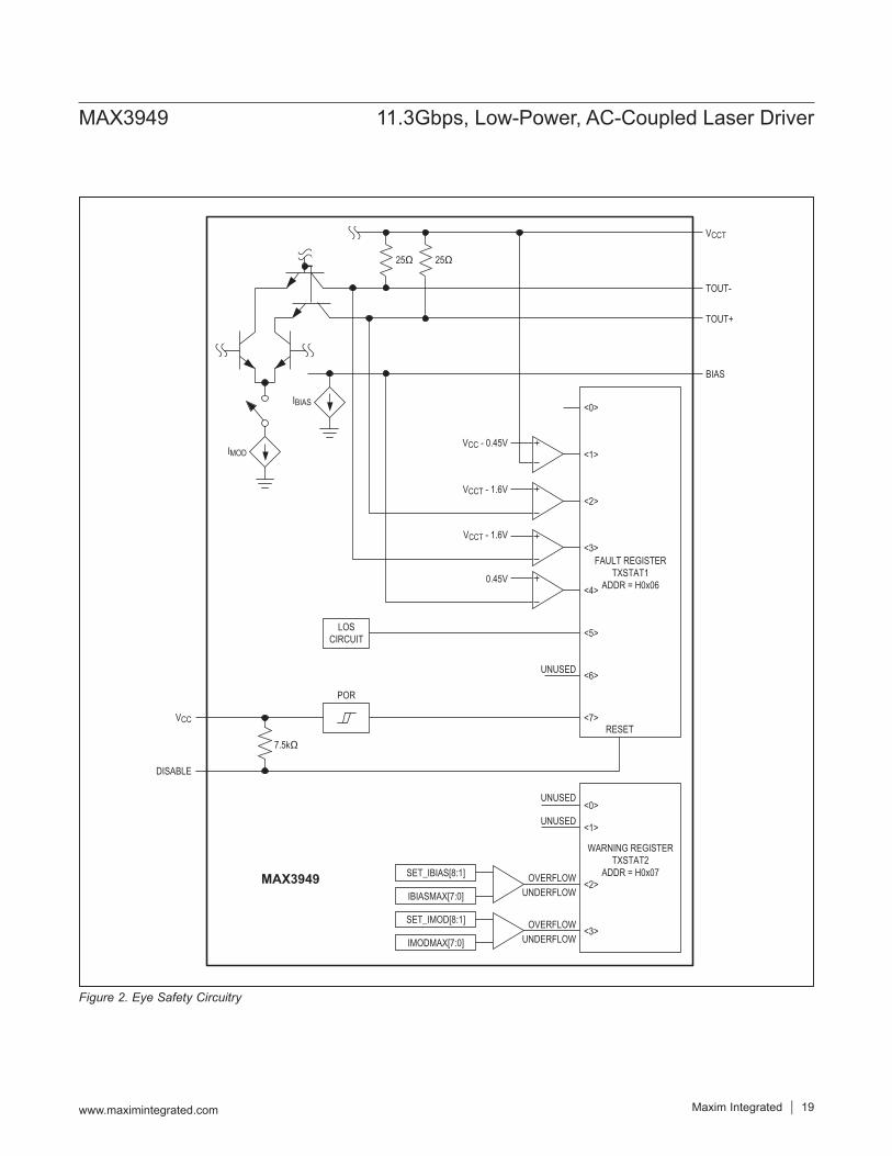
Figure 2. Eye Safety Circuitry
MAX3949 11.3Gbps, Low-Power, AC-Coupled Laser Driver
www.maximintegrated.com Maxim Integrated 19
<0>
<1>VCC - 0.45V
IMOD
IBIAS
<2>VCCT - 1.6V
<3>
<4>
<6>
<7>
0.45V
<5>
VCCT - 1.6V
UNUSED
FAULT REGISTERTXSTAT1
ADDR = H0x06
<1>
<0>UNUSED
UNUSED
OVERFLOWUNDERFLOW
SET_IBIAS[8:1]
IBIASMAX[7:0]
SET_IMOD[8:1]
IMODMAX[7:0]
LOSCIRCUIT
OVERFLOWUNDERFLOW
<2>
<3>
WARNING REGISTERTXSTAT2
ADDR = H0x07
VCCT
TOUT-
VCC
DISABLE
7.5kΩRESET
POR
25Ω
TOUT+
BIAS
MAX3949
25Ω
Note 1: Normal operation—Does not affect the laser power.Note 2: Pin functionality might be affected, which could affect laser power/performance.Note 3: Supply-shorted current is assumed to be primarily on the circuit board (outside this device) and the main supply is collapsed
by the short.Note 4: Normal in functionality, but performance could be affected.Warning: Shorted to VCC or shorted to ground on some pins can violate the Absolute Maximum Ratings.
The FAULT pin is a latched output that can be cleared by toggling the DISABLE pin. Toggling the DISABLE pin also clears the TXSTAT1 and TXSTAT2 registers. A single-point
failure can be a short to VCC or GND. Table 3 shows the circuit response to various single-point failures.
Table 3. Circuit Response to Single-Point Failure
PIN NAME SHORT TO VCC SHORT TO GND OPEN
1 DISABLE Disabled Normal (Note 1). Can only be disabled by other means. Disabled
2 VSEL Normal (Note 2) Normal (Note 2) Normal (Note 2)
3 FAULT Normal (Note 2) Normal (Note 1) Normal (Note 2)
4 BMON Normal (Note 2) Normal (Note 2) Normal (Note 2)
5, 8 VCCT Normal Disabled—Fault (external supply shorted) (Note 3) Redundant path (Note 4)
6 TOUT- Laser modulation current is reduced Disabled (hard fault) Laser modulation current is
reduced or disabled (hard fault)
7 TOUT+ Laser modulation current is reduced or off Disabled (hard fault) Laser modulation current is
reduced or disabled (hard fault)
9 BIAS IBIAS is on, but not delivered to the laser; no fault Disabled (hard fault) Disabled (hard fault)
10 CSEL Normal (Note 2) Normal (Note 2) Normal (Note 2)
11 SDA Normal (Note 2) Normal (Note 2) Normal (Note 2)
12 SCL Normal (Note 2) Normal (Note 2) Normal (Note 2)
13, 16 VCC Normal Disabled—Hard fault (external supply shorted) (Note 3) Redundant path (Note 4)
14 TIN+ Disabled (hard fault) Disabled (hard fault) Normal (Note 2) or disabled (hard fault)
15 TIN- Disabled (hard fault) Disabled (hard fault) Normal (Note 2) or disabled (hard fault)
MAX3949 11.3Gbps, Low-Power, AC-Coupled Laser Driver
www.maximintegrated.com Maxim Integrated 20
3-Wire InterfaceThe MAX3949 implements a proprietary 3-wire digital interface. An external controller generates the clock. The 3-wire interface consists of an SDA bidirectional data line, a SCL clock signal input, and a CSEL chip-select input (active high). The external master initiates a data transfer by asserting the CSEL pin. The master starts to generate a clock signal after the CSEL pin has been set to a logic-high. All data transfers are most significant bit (MSB) first.
ProtocolEach operation consists of 16-bit transfers (15-bit address/data, 1-bit RWN). The bus master generates 16 clock cycles to SCL. All operations transfer 8 bits to the MAX3949. The RWN bit determines if the cycle is read or write (Table 5).
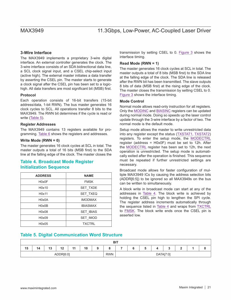
Register AddressesThe MAX3949 contains 13 registers available for pro-gramming. Table 6 shows the registers and addresses.
Write Mode (RWN = 0)The master generates 16 clock cycles at SCL in total. The master outputs a total of 16 bits (MSB first) to the SDA line at the falling edge of the clock. The master closes the
transmission by setting CSEL to 0. Figure 3 shows the interface timing.
Read Mode (RWN = 1)The master generates 16 clock cycles at SCL in total. The master outputs a total of 8 bits (MSB first) to the SDA line at the falling edge of the clock. The SDA line is released after the RWN bit has been transmitted. The slave outputs 8 bits of data (MSB first) at the rising edge of the clock. The master closes the transmission by setting CSEL to 0. Figure 3 shows the interface timing.
Mode ControlNormal mode allows read-only instruction for all registers. Only the MODINC and BIASINC registers can be updated during normal mode. Doing so speeds up the laser control update through the 3-wire interface by a factor of two. The normal mode is the default mode.Setup mode allows the master to write unrestricted data into any register except the status (TXSTAT1, TXSTAT2) registers. To enter the setup mode, the MODECTRL register (address = H0x0F) must be set to 12h. After the MODECTRL register has been set to 12h, the next operation is unrestricted. The setup mode is automati-cally exited after the operation is finished. This sequence must be repeated if further unrestricted settings are necessary.Broadcast mode allows for faster configuration of mul-tiple MAX3949 ICs by causing the address selection bits (ADDR[6:5]) to be ignored so all MAX3949s on the bus can be written to simultaneously.A block write in broadcast mode can start at any of the addresses in Table 4. The block write is achieved by holding the CSEL pin high to lengthen the SPI cycle. The register address increments automatically through the sequence listed in Table 4 and wraps from TXCTRL to FMSK. The block write ends once the CSEL pin is asserted low.
Table 5. Digital Communication Word Structure
Table 4. Broadcast Mode Register Initialization Sequence
ADDRESS NAME
H0x0F FMSK
H0x10 SET_TXDE
H0x11 SET_TXEQ
H0x0A IMODMAX
H0x0B IBIASMAX
H0x08 SET_IBIAS
H0x09 SET_IMOD
H0x05 TXCTRL
BIT
15 14 13 12 11 10 9 8 7 6 5 4 3 2 1 0
ADDR[6:0] RWN DATA[7:0]
MAX3949 11.3Gbps, Low-Power, AC-Coupled Laser Driver
www.maximintegrated.com Maxim Integrated 21
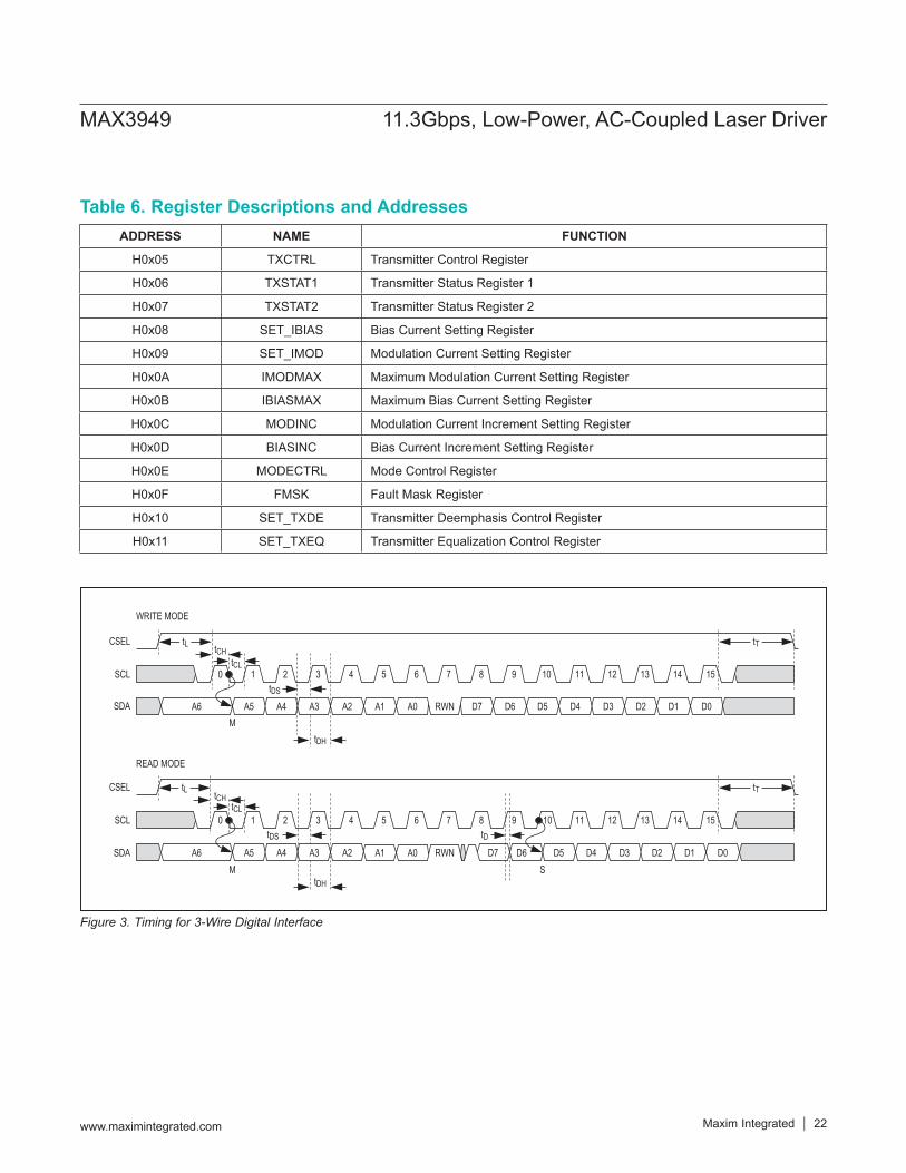
Table 6. Register Descriptions and Addresses
Figure 3. Timing for 3-Wire Digital Interface
ADDRESS NAME FUNCTION
H0x05 TXCTRL Transmitter Control Register
H0x06 TXSTAT1 Transmitter Status Register 1
H0x07 TXSTAT2 Transmitter Status Register 2
H0x08 SET_IBIAS Bias Current Setting Register
H0x09 SET_IMOD Modulation Current Setting Register
H0x0A IMODMAX Maximum Modulation Current Setting Register
H0x0B IBIASMAX Maximum Bias Current Setting Register
H0x0C MODINC Modulation Current Increment Setting Register
H0x0D BIASINC Bias Current Increment Setting Register
H0x0E MODECTRL Mode Control Register
H0x0F FMSK Fault Mask Register
H0x10 SET_TXDE Transmitter Deemphasis Control Register
H0x11 SET_TXEQ Transmitter Equalization Control Register
MAX3949 11.3Gbps, Low-Power, AC-Coupled Laser Driver
www.maximintegrated.com Maxim Integrated 22
CSEL
SCL
SDA
CSEL
SCL
SDA
1 2 3 4 5 6 7 8
A6
9 10 11 12 13 14 150
1 2 3 4 5 6 7 8 9 10 11 12 13 14 150
A5 A4 A3 A2 A1 RWN D7 D6 D5 D4 D3 D2 D1 D0
D7 D6 D5 D4 D3 D2 D1 D0RWN
WRITE MODE
READ MODE
A0
A6 A5 A4 A3 A2 A1 A0
tL
tL
tCHtCL
tDS
tDH
M
tCHtCL
tDS tD
tDH
tT
tT
M S
Register DescriptionsTransmitter Control Register (TXCTRL), Address: H0x05
Bit D7 D6 D5 D4 D3 D2 D1 D0
Bit Name RESERVED RESERVED RESERVED TXDE_MD[1] TXDE_MD[0] SOFTRES TX_POL TX_EN
Read/Write R/W R/W R/W R/W R/W R/W R/W R/W
POR State 0 0 0 0 0 0 1 0
The TXCTRL register sets the device’s operation.
BIT NAME DESCRIPTION
D[7:5] RESERVED Reserved Bits. The default state for these bits is 0 and they must be kept 0 when the register is accessed for a write operation.
D[4:3] TXDE_MD
Controls the mode of the transmit output deemphasis circuitry. 00 = Deemphasis is fixed at 6% of the modulation amplitude 01 = Deemphasis is fixed at 3% of the modulation amplitude 10 = Deemphasis is programmed by SET_TXDE register setting (3% to 9%) 11 = Deemphasis is at its maximum of ~9%
D2 SOFTRES
Resets all registers to their default values (TXCTRL[1:0] must be = 10b during the write to SOFTRES for the registers to be set to their default values). 0 = Normal operation 1 = Reset
D1 TX_POLControls the polarity of the transmit signal path. 0 = Inverse 1 = Normal operation
D0 TX_ENEnables or disables the transmit circuitry. 0 = Disabled 1 = Enabled
MAX3949 11.3Gbps, Low-Power, AC-Coupled Laser Driver
www.maximintegrated.com Maxim Integrated 23
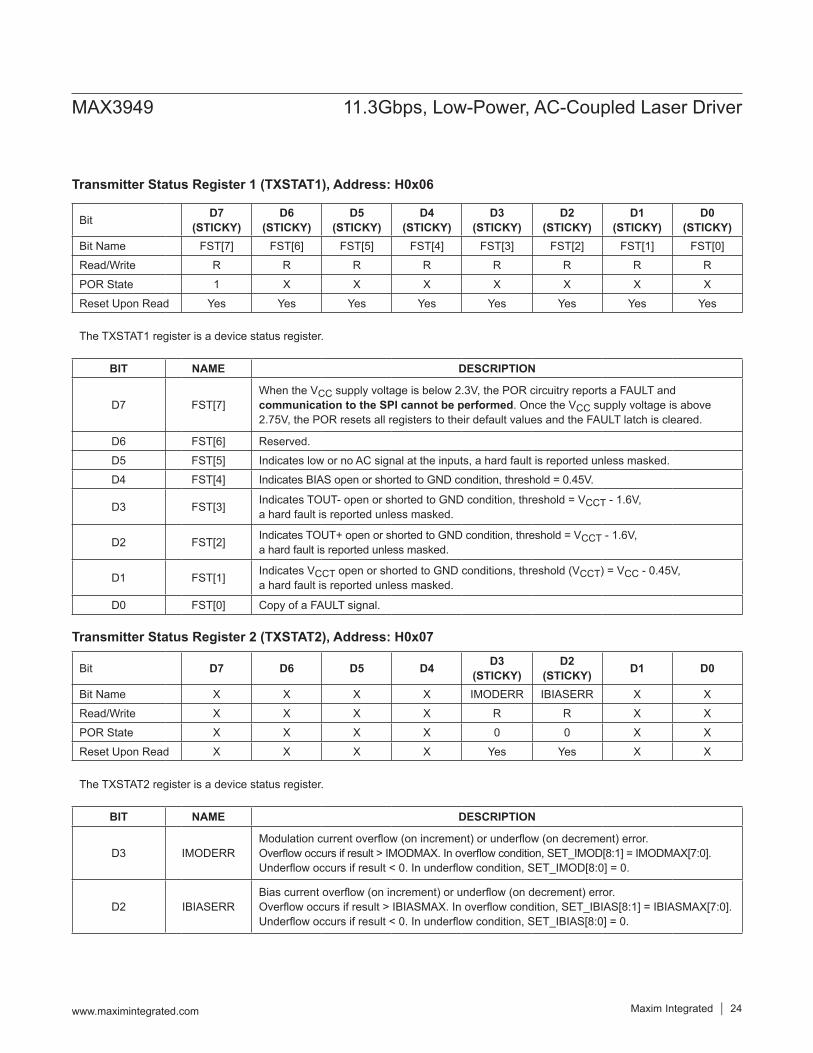
Transmitter Status Register 1 (TXSTAT1), Address: H0x06
Transmitter Status Register 2 (TXSTAT2), Address: H0x07
Bit D7 (STICKY)
D6 (STICKY)
D5 (STICKY)
D4 (STICKY)
D3 (STICKY)
D2 (STICKY)
D1 (STICKY)
D0 (STICKY)
Bit Name FST[7] FST[6] FST[5] FST[4] FST[3] FST[2] FST[1] FST[0]Read/Write R R R R R R R RPOR State 1 X X X X X X XReset Upon Read Yes Yes Yes Yes Yes Yes Yes Yes
The TXSTAT1 register is a device status register.
BIT NAME DESCRIPTION
D7 FST[7]When the VCC supply voltage is below 2.3V, the POR circuitry reports a FAULT and communication to the SPI cannot be performed. Once the VCC supply voltage is above 2.75V, the POR resets all registers to their default values and the FAULT latch is cleared.
D6 FST[6] Reserved.D5 FST[5] Indicates low or no AC signal at the inputs, a hard fault is reported unless masked.D4 FST[4] Indicates BIAS open or shorted to GND condition, threshold = 0.45V.
D3 FST[3] Indicates TOUT- open or shorted to GND condition, threshold = VCCT - 1.6V, a hard fault is reported unless masked.
D2 FST[2] Indicates TOUT+ open or shorted to GND condition, threshold = VCCT - 1.6V, a hard fault is reported unless masked.
D1 FST[1] Indicates VCCT open or shorted to GND conditions, threshold (VCCT) = VCC - 0.45V, a hard fault is reported unless masked.
D0 FST[0] Copy of a FAULT signal.
Bit D7 D6 D5 D4 D3 (STICKY)
D2 (STICKY) D1 D0
Bit Name X X X X IMODERR IBIASERR X XRead/Write X X X X R R X XPOR State X X X X 0 0 X XReset Upon Read X X X X Yes Yes X X
The TXSTAT2 register is a device status register.
BIT NAME DESCRIPTION
D3 IMODERRModulation current overflow (on increment) or underflow (on decrement) error. Overflow occurs if result > IMODMAX. In overflow condition, SET_IMOD[8:1] = IMODMAX[7:0]. Underflow occurs if result < 0. In underflow condition, SET_IMOD[8:0] = 0.
D2 IBIASERRBias current overflow (on increment) or underflow (on decrement) error. Overflow occurs if result > IBIASMAX. In overflow condition, SET_IBIAS[8:1] = IBIASMAX[7:0]. Underflow occurs if result < 0. In underflow condition, SET_IBIAS[8:0] = 0.
MAX3949 11.3Gbps, Low-Power, AC-Coupled Laser Driver
www.maximintegrated.com Maxim Integrated 24
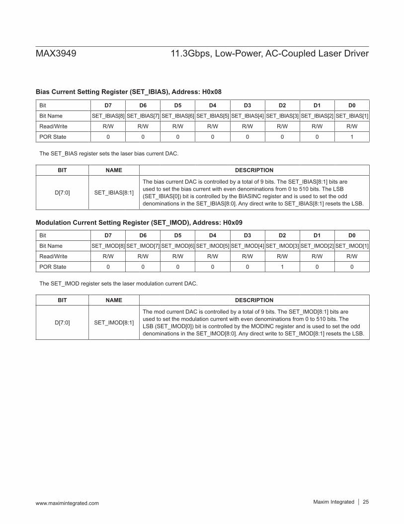
Bias Current Setting Register (SET_IBIAS), Address: H0x08
Modulation Current Setting Register (SET_IMOD), Address: H0x09
Bit D7 D6 D5 D4 D3 D2 D1 D0
Bit Name SET_IBIAS[8] SET_IBIAS[7] SET_IBIAS[6] SET_IBIAS[5] SET_IBIAS[4] SET_IBIAS[3] SET_IBIAS[2] SET_IBIAS[1]
Read/Write R/W R/W R/W R/W R/W R/W R/W R/W
POR State 0 0 0 0 0 0 0 1
The SET_BIAS register sets the laser bias current DAC.
BIT NAME DESCRIPTION
D[7:0] SET_IBIAS[8:1]
The bias current DAC is controlled by a total of 9 bits. The SET_IBIAS[8:1] bits are used to set the bias current with even denominations from 0 to 510 bits. The LSB (SET_IBIAS[0]) bit is controlled by the BIASINC register and is used to set the odd denominations in the SET_IBIAS[8:0]. Any direct write to SET_IBIAS[8:1] resets the LSB.
Bit D7 D6 D5 D4 D3 D2 D1 D0
Bit Name SET_IMOD[8] SET_IMOD[7] SET_IMOD[6] SET_IMOD[5] SET_IMOD[4] SET_IMOD[3] SET_IMOD[2] SET_IMOD[1]
Read/Write R/W R/W R/W R/W R/W R/W R/W R/W
POR State 0 0 0 0 0 1 0 0
The SET_IMOD register sets the laser modulation current DAC.
BIT NAME DESCRIPTION
D[7:0] SET_IMOD[8:1]
The mod current DAC is controlled by a total of 9 bits. The SET_IMOD[8:1] bits are used to set the modulation current with even denominations from 0 to 510 bits. The LSB (SET_IMOD[0]) bit is controlled by the MODINC register and is used to set the odd denominations in the SET_IMOD[8:0]. Any direct write to SET_IMOD[8:1] resets the LSB.
MAX3949 11.3Gbps, Low-Power, AC-Coupled Laser Driver
www.maximintegrated.com Maxim Integrated 25
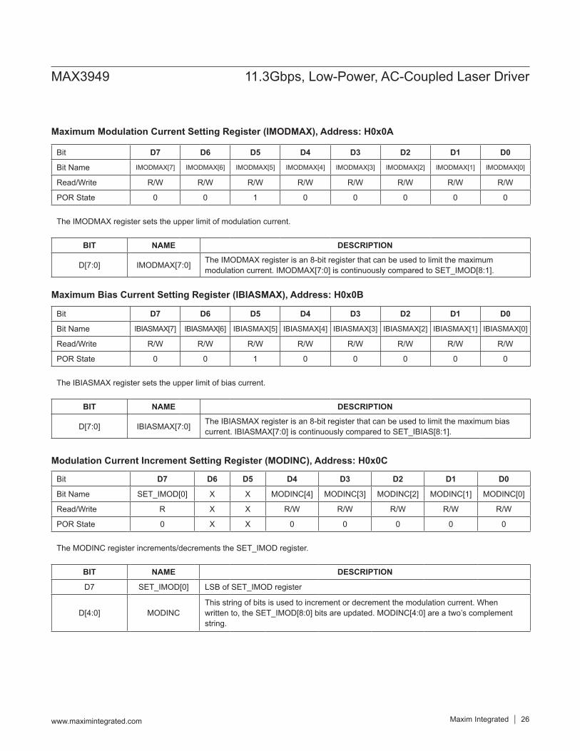
Maximum Modulation Current Setting Register (IMODMAX), Address: H0x0A
Maximum Bias Current Setting Register (IBIASMAX), Address: H0x0B
Modulation Current Increment Setting Register (MODINC), Address: H0x0C
Bit D7 D6 D5 D4 D3 D2 D1 D0
Bit Name IMODMAX[7] IMODMAX[6] IMODMAX[5] IMODMAX[4] IMODMAX[3] IMODMAX[2] IMODMAX[1] IMODMAX[0]
Read/Write R/W R/W R/W R/W R/W R/W R/W R/W
POR State 0 0 1 0 0 0 0 0
The IMODMAX register sets the upper limit of modulation current.
BIT NAME DESCRIPTION
D[7:0] IMODMAX[7:0] The IMODMAX register is an 8-bit register that can be used to limit the maximum modulation current. IMODMAX[7:0] is continuously compared to SET_IMOD[8:1].
Bit D7 D6 D5 D4 D3 D2 D1 D0
Bit Name IBIASMAX[7] IBIASMAX[6] IBIASMAX[5] IBIASMAX[4] IBIASMAX[3] IBIASMAX[2] IBIASMAX[1] IBIASMAX[0]
Read/Write R/W R/W R/W R/W R/W R/W R/W R/W
POR State 0 0 1 0 0 0 0 0
The IBIASMAX register sets the upper limit of bias current.
BIT NAME DESCRIPTION
D[7:0] IBIASMAX[7:0] The IBIASMAX register is an 8-bit register that can be used to limit the maximum bias current. IBIASMAX[7:0] is continuously compared to SET_IBIAS[8:1].
Bit D7 D6 D5 D4 D3 D2 D1 D0
Bit Name SET_IMOD[0] X X MODINC[4] MODINC[3] MODINC[2] MODINC[1] MODINC[0]
Read/Write R X X R/W R/W R/W R/W R/W
POR State 0 X X 0 0 0 0 0
The MODINC register increments/decrements the SET_IMOD register.
BIT NAME DESCRIPTION
D7 SET_IMOD[0] LSB of SET_IMOD register
D[4:0] MODINCThis string of bits is used to increment or decrement the modulation current. When written to, the SET_IMOD[8:0] bits are updated. MODINC[4:0] are a two’s complement string.
MAX3949 11.3Gbps, Low-Power, AC-Coupled Laser Driver
www.maximintegrated.com Maxim Integrated 26
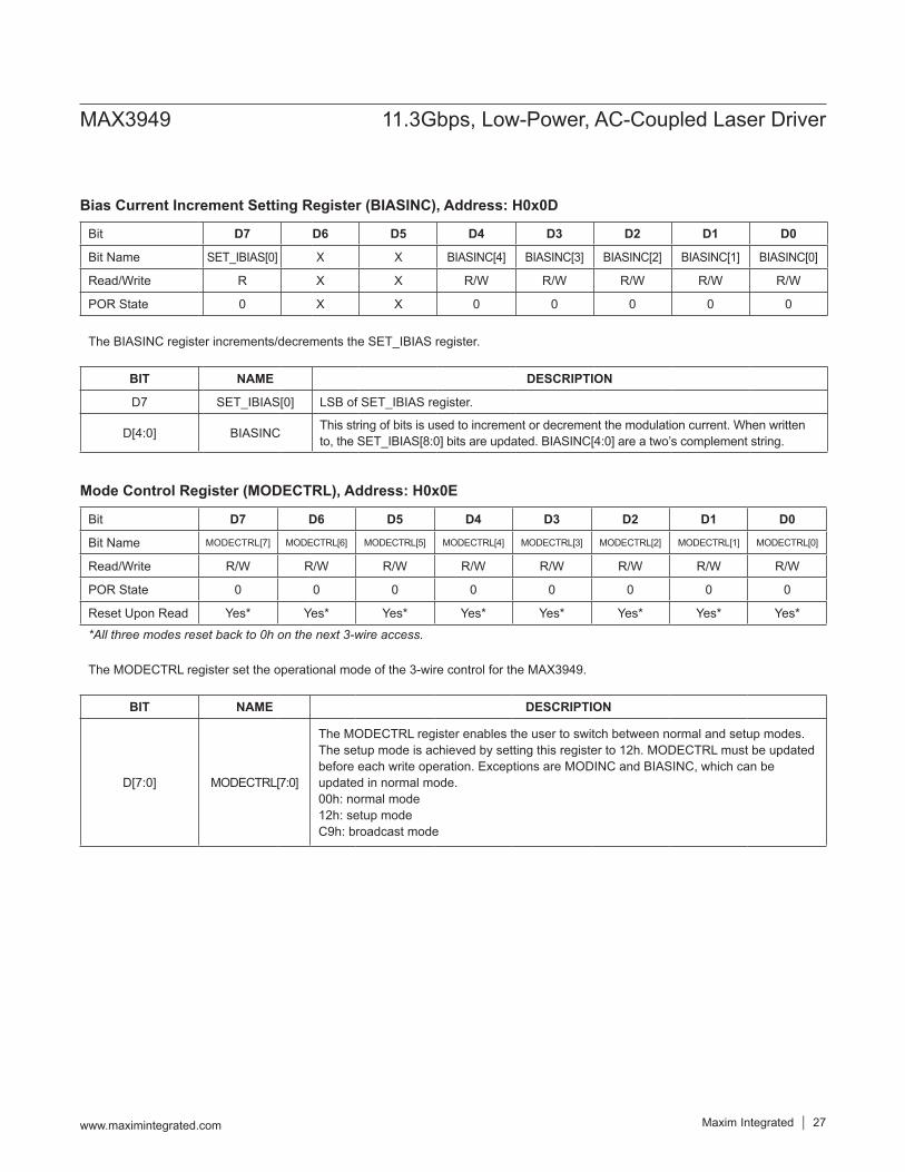
Bias Current Increment Setting Register (BIASINC), Address: H0x0D
Mode Control Register (MODECTRL), Address: H0x0E
Bit D7 D6 D5 D4 D3 D2 D1 D0
Bit Name SET_IBIAS[0] X X BIASINC[4] BIASINC[3] BIASINC[2] BIASINC[1] BIASINC[0]
Read/Write R X X R/W R/W R/W R/W R/W
POR State 0 X X 0 0 0 0 0
The BIASINC register increments/decrements the SET_IBIAS register.
BIT NAME DESCRIPTION
D7 SET_IBIAS[0] LSB of SET_IBIAS register.
D[4:0] BIASINC This string of bits is used to increment or decrement the modulation current. When written to, the SET_IBIAS[8:0] bits are updated. BIASINC[4:0] are a two’s complement string.
Bit D7 D6 D5 D4 D3 D2 D1 D0
Bit Name MODECTRL[7] MODECTRL[6] MODECTRL[5] MODECTRL[4] MODECTRL[3] MODECTRL[2] MODECTRL[1] MODECTRL[0]
Read/Write R/W R/W R/W R/W R/W R/W R/W R/W
POR State 0 0 0 0 0 0 0 0
Reset Upon Read Yes* Yes* Yes* Yes* Yes* Yes* Yes* Yes*
*All three modes reset back to 0h on the next 3-wire access.
The MODECTRL register set the operational mode of the 3-wire control for the MAX3949.
BIT NAME DESCRIPTION
D[7:0] MODECTRL[7:0]
The MODECTRL register enables the user to switch between normal and setup modes. The setup mode is achieved by setting this register to 12h. MODECTRL must be updated before each write operation. Exceptions are MODINC and BIASINC, which can be updated in normal mode. 00h: normal mode 12h: setup mode C9h: broadcast mode
MAX3949 11.3Gbps, Low-Power, AC-Coupled Laser Driver
www.maximintegrated.com Maxim Integrated 27
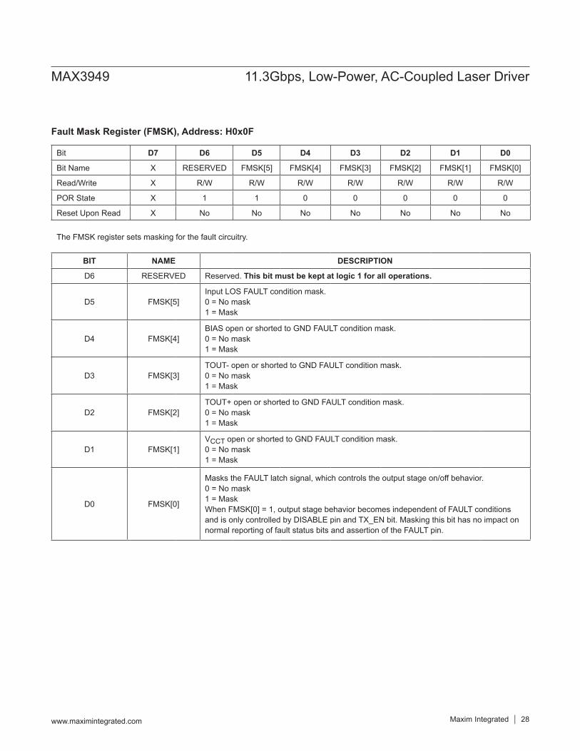
Fault Mask Register (FMSK), Address: H0x0F
Bit D7 D6 D5 D4 D3 D2 D1 D0
Bit Name X RESERVED FMSK[5] FMSK[4] FMSK[3] FMSK[2] FMSK[1] FMSK[0]
Read/Write X R/W R/W R/W R/W R/W R/W R/W
POR State X 1 1 0 0 0 0 0
Reset Upon Read X No No No No No No No
The FMSK register sets masking for the fault circuitry.
BIT NAME DESCRIPTION
D6 RESERVED Reserved. This bit must be kept at logic 1 for all operations.
D5 FMSK[5]Input LOS FAULT condition mask. 0 = No mask 1 = Mask
D4 FMSK[4]BIAS open or shorted to GND FAULT condition mask. 0 = No mask 1 = Mask
D3 FMSK[3]TOUT- open or shorted to GND FAULT condition mask. 0 = No mask 1 = Mask
D2 FMSK[2]TOUT+ open or shorted to GND FAULT condition mask. 0 = No mask 1 = Mask
D1 FMSK[1]VCCT open or shorted to GND FAULT condition mask. 0 = No mask 1 = Mask
D0 FMSK[0]
Masks the FAULT latch signal, which controls the output stage on/off behavior. 0 = No mask 1 = Mask When FMSK[0] = 1, output stage behavior becomes independent of FAULT conditions and is only controlled by DISABLE pin and TX_EN bit. Masking this bit has no impact on normal reporting of fault status bits and assertion of the FAULT pin.
MAX3949 11.3Gbps, Low-Power, AC-Coupled Laser Driver
www.maximintegrated.com Maxim Integrated 28
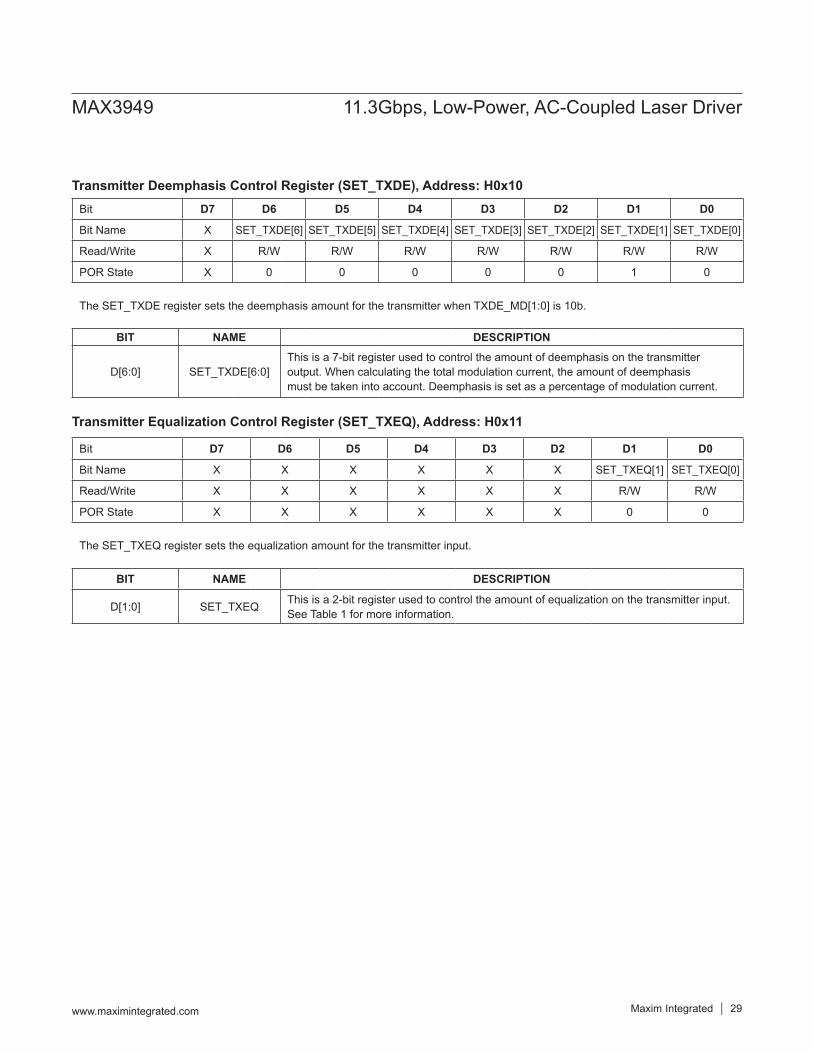
Transmitter Deemphasis Control Register (SET_TXDE), Address: H0x10
Transmitter Equalization Control Register (SET_TXEQ), Address: H0x11
Bit D7 D6 D5 D4 D3 D2 D1 D0
Bit Name X SET_TXDE[6] SET_TXDE[5] SET_TXDE[4] SET_TXDE[3] SET_TXDE[2] SET_TXDE[1] SET_TXDE[0]
Read/Write X R/W R/W R/W R/W R/W R/W R/W
POR State X 0 0 0 0 0 1 0
The SET_TXDE register sets the deemphasis amount for the transmitter when TXDE_MD[1:0] is 10b.
BIT NAME DESCRIPTION
D[6:0] SET_TXDE[6:0]This is a 7-bit register used to control the amount of deemphasis on the transmitter output. When calculating the total modulation current, the amount of deemphasis must be taken into account. Deemphasis is set as a percentage of modulation current.
Bit D7 D6 D5 D4 D3 D2 D1 D0
Bit Name X X X X X X SET_TXEQ[1] SET_TXEQ[0]
Read/Write X X X X X X R/W R/W
POR State X X X X X X 0 0
The SET_TXEQ register sets the equalization amount for the transmitter input.
BIT NAME DESCRIPTION
D[1:0] SET_TXEQ This is a 2-bit register used to control the amount of equalization on the transmitter input. See Table 1 for more information.
MAX3949 11.3Gbps, Low-Power, AC-Coupled Laser Driver
www.maximintegrated.com Maxim Integrated 29
Design ProcedureProgramming Modulation Current1) IMODMAX[7:0] = Maximum_Modulation_Current_
Value2) SET_IMODn[8:0] = Present_Modulation_Current_
Value Note: SET_IMOD[8:1] are the bits that can be manu-
ally written. SET_IMOD[0] can only be updated using the MODINC register.
When implementing modulation current temperature compensation, it is recommended to use the MODINC register, which guarantees the fastest modulation cur-rent update.
3) MODINCn[4:0] = New_Increment_Value The device performs the following operation when
MODINCn[4:0] is written to:If (SET_IMODn[8:1] ≤ IMODMAX[7:0]), then(SET_IMODn[8:0] = SET_IMODn-1[8:0] + MODINCn[4:0])else (SET_IMODn[8:1] = IMODMAX[7:0])
The modulation DAC current can be calculated using the following equation:
IMOD DAC Current = IMOD = (16 + SET_IMOD[8:0]) x 247µA
The net modulation current (P-P) seen at the laser when driven differentially is calculated using the fol-lowing equation:
LDMOD = IMOD x (1 - DE) x 50/(50 + R) where R is the differential load impedance of the laser
plus any added series resistance, and DE is the deem-phasis factor controlled by the TX_DEMD[1:0] bits.
4) TXCTRL[4:3] = 00, DE = 0.0625 (~ 6% deemphasis case). In this mode, the device calculates and sets SET_TXDE[6:0] = SET_IMOD[8:2]. SET_TXDE is not accessible for external write.
5) TXCTRL[4:3] = 00, DE = 0.03125 (~ 3% deemphasis case). In this mode, the device calculates and sets SET_TXDE[6:0] = SET_IMOD[8:3]. SET_TXDE is not accessible for external write.
6) TXCTRL[4:3] = 00, SET_TXDE can be externally set to any value ≥ SET_IMOD[8:3]:
IDE = (2 + SET_TXDE[6:0]) x 61.8µA In this case DE = IDE/IMOD. The value of the DE factor
starts close to 0.03 and can go up to 0.09 as the value of SET_TXDE[6:0] is increased. Once the DE ratio is close to 0.09, the IDE saturates and a further increase in SET_TXDE[6:0] value does not change IDE much.
7) TXCTRL[4:3] = 11, DE = 0.09 (~ 9% deemphasis case). In this mode, the device calculates and sets the SET_TXDE[6:0] = 127. SET_TXDE is not accessible for external write.
Programming Bias Current1) IBIASMAX[7:0] = Maximum_Bias_Current_Value2) SET_IBIASn[8:0] = Present_ Bias_Current_Value Note: SET_IBIAS[8:1] are the bits that can be
manually written. SET_IBIAS[0] can only be updated using the BIASINC register.
When implementing laser bias current temperature compensation, it is recommended to use the BIASINC register, which guarantees the fastest modulation current update.
3) BIASINCn[4:0] = New_Increment_Value The device performs the following operation when
BIASINCn[4:0] is written to:If (SET_IBIASn[8:1] ≤ IBIASMAX[7:0]), then(SET_IBIASn[8:0] = SET_IBIASn-1[8:0] + BIASINCn[4:0])else (SET_IBIASn[8:1] = IBIASMAX[7:0])
The bias DAC current can be calculated using the following equation:
BIAS DAC Current = IBIAS = (16 + SET_IBIAS[8:0]) x 200µA
MAX3949 11.3Gbps, Low-Power, AC-Coupled Laser Driver
www.maximintegrated.com Maxim Integrated 30
Applications InformationLaser Safety and IEC 825Using the MAX3949 laser driver alone does not ensure that a transmitter design is compliant with IEC 825. The entire transmitter circuit and component selections must be considered. Each user must determine the level of
fault tolerance required by the application, recognizing that Maxim products are neither designed nor authorized for use as components in systems intended for surgical implant into the body, for applications intended to support or sustain life, or for any other application in which the failure of a Maxim product could create a situation where personal injury or death could occur.
Table 7. Register SummaryREGISTER FUNCTION/ ADDRESS
REGISTER NAME
NORMAL MODE
SETUP MODE
BIT NUMBER/
TYPEBIT NAME DEFAULT
VALUE NOTES
Transmitter Control Register Address = H0x05
TXCTRL
R R/W 7 Reserved 0 Must be kept at 0
R R/W 6 Reserved 0 Must be kept at 0
R R/W 5 Reserved 0 Must be kept at 0
R R/W 4 TXDE_MD[1] 0 Tx deemphasis control
R R/W 3 TXDE_MD[0] 0 Tx deemphasis control
R R/W 2 SOFTRES 0 Global digital reset
R R/W 1 TX_POL 1 Tx polarity 0: inverse, 1: normal
R R/W 0 TX_EN 0 Tx control 0: disable, 1: enable
Transmitter Status Register 1 Address = H0x06
TXSTAT1
R R 7 (sticky) FST[7] 1 PORàVCC low-limit violation
R R 6 (sticky) FST[6] X Reserved
R R 5 (sticky) FST[5] X Low or no AC signal at input
R R 4 (sticky) FST[4] X BIAS open or shorted to GND
R R 3 (sticky) FST[3] X TOUT- open or shorted to GND
R R 2 (sticky) FST[2] X TOUT+ open or shorted to GND
R R 1 (sticky) FST[1] X VCCT open or shorted to GND
R R 0 (sticky) FST[0] X Copy of FAULT signal
MAX3949 11.3Gbps, Low-Power, AC-Coupled Laser Driver
www.maximintegrated.com Maxim Integrated 31
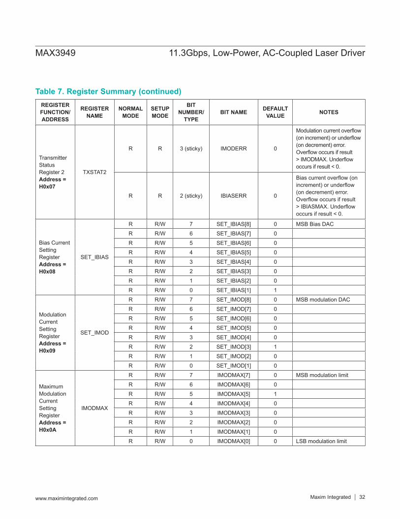
Table 7. Register Summary (continued)REGISTER FUNCTION/ ADDRESS
REGISTER NAME
NORMAL MODE
SETUP MODE
BIT NUMBER/
TYPEBIT NAME DEFAULT
VALUE NOTES
Transmitter Status Register 2 Address = H0x07
TXSTAT2
R R 3 (sticky) IMODERR 0
Modulation current overflow (on increment) or underflow (on decrement) error. Overflow occurs if result > IMODMAX. Underflow occurs if result < 0.
R R 2 (sticky) IBIASERR 0
Bias current overflow (on increment) or underflow (on decrement) error. Overflow occurs if result > IBIASMAX. Underflow occurs if result < 0.
Bias Current Setting Register Address = H0x08
SET_IBIAS
R R/W 7 SET_IBIAS[8] 0 MSB Bias DACR R/W 6 SET_IBIAS[7] 0R R/W 5 SET_IBIAS[6] 0R R/W 4 SET_IBIAS[5] 0R R/W 3 SET_IBIAS[4] 0R R/W 2 SET_IBIAS[3] 0R R/W 1 SET_IBIAS[2] 0R R/W 0 SET_IBIAS[1] 1
Modulation Current Setting Register Address = H0x09
SET_IMOD
R R/W 7 SET_IMOD[8] 0 MSB modulation DACR R/W 6 SET_IMOD[7] 0R R/W 5 SET_IMOD[6] 0R R/W 4 SET_IMOD[5] 0R R/W 3 SET_IMOD[4] 0R R/W 2 SET_IMOD[3] 1R R/W 1 SET_IMOD[2] 0R R/W 0 SET_IMOD[1] 0
Maximum Modulation Current Setting Register Address = H0x0A
IMODMAX
R R/W 7 IMODMAX[7] 0 MSB modulation limitR R/W 6 IMODMAX[6] 0R R/W 5 IMODMAX[5] 1R R/W 4 IMODMAX[4] 0R R/W 3 IMODMAX[3] 0R R/W 2 IMODMAX[2] 0R R/W 1 IMODMAX[1] 0R R/W 0 IMODMAX[0] 0 LSB modulation limit
MAX3949 11.3Gbps, Low-Power, AC-Coupled Laser Driver
www.maximintegrated.com Maxim Integrated 32
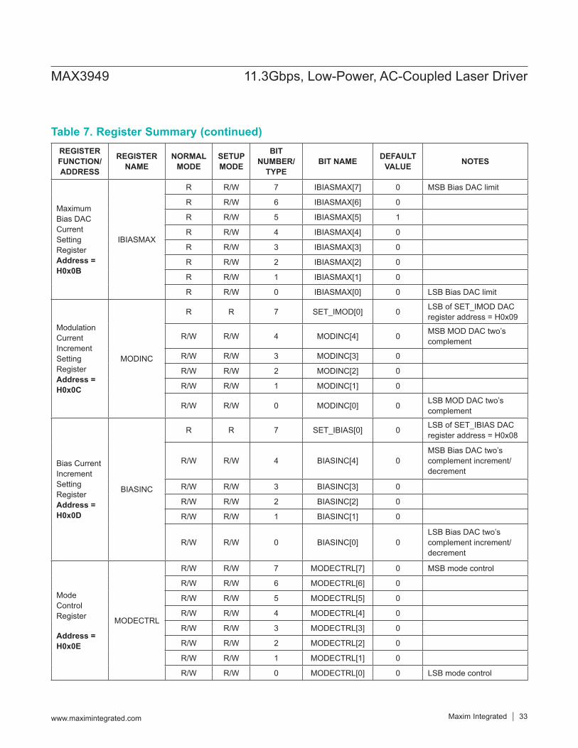
Table 7. Register Summary (continued)REGISTER FUNCTION/ ADDRESS
REGISTER NAME
NORMAL MODE
SETUP MODE
BIT NUMBER/
TYPEBIT NAME DEFAULT
VALUE NOTES
Maximum Bias DAC Current Setting Register Address = H0x0B
IBIASMAX
R R/W 7 IBIASMAX[7] 0 MSB Bias DAC limit
R R/W 6 IBIASMAX[6] 0
R R/W 5 IBIASMAX[5] 1
R R/W 4 IBIASMAX[4] 0
R R/W 3 IBIASMAX[3] 0
R R/W 2 IBIASMAX[2] 0
R R/W 1 IBIASMAX[1] 0
R R/W 0 IBIASMAX[0] 0 LSB Bias DAC limit
Modulation Current Increment Setting Register Address = H0x0C
MODINC
R R 7 SET_IMOD[0] 0 LSB of SET_IMOD DAC register address = H0x09
R/W R/W 4 MODINC[4] 0 MSB MOD DAC two’s complement
R/W R/W 3 MODINC[3] 0
R/W R/W 2 MODINC[2] 0
R/W R/W 1 MODINC[1] 0
R/W R/W 0 MODINC[0] 0 LSB MOD DAC two’s complement
Bias Current Increment Setting Register Address = H0x0D
BIASINC
R R 7 SET_IBIAS[0] 0 LSB of SET_IBIAS DAC register address = H0x08
R/W R/W 4 BIASINC[4] 0MSB Bias DAC two’s complement increment/decrement
R/W R/W 3 BIASINC[3] 0
R/W R/W 2 BIASINC[2] 0
R/W R/W 1 BIASINC[1] 0
R/W R/W 0 BIASINC[0] 0LSB Bias DAC two’s complement increment/decrement
Mode Control Register
Address = H0x0E
MODECTRL
R/W R/W 7 MODECTRL[7] 0 MSB mode control
R/W R/W 6 MODECTRL[6] 0
R/W R/W 5 MODECTRL[5] 0
R/W R/W 4 MODECTRL[4] 0
R/W R/W 3 MODECTRL[3] 0
R/W R/W 2 MODECTRL[2] 0
R/W R/W 1 MODECTRL[1] 0
R/W R/W 0 MODECTRL[0] 0 LSB mode control
MAX3949 11.3Gbps, Low-Power, AC-Coupled Laser Driver
www.maximintegrated.com Maxim Integrated 33
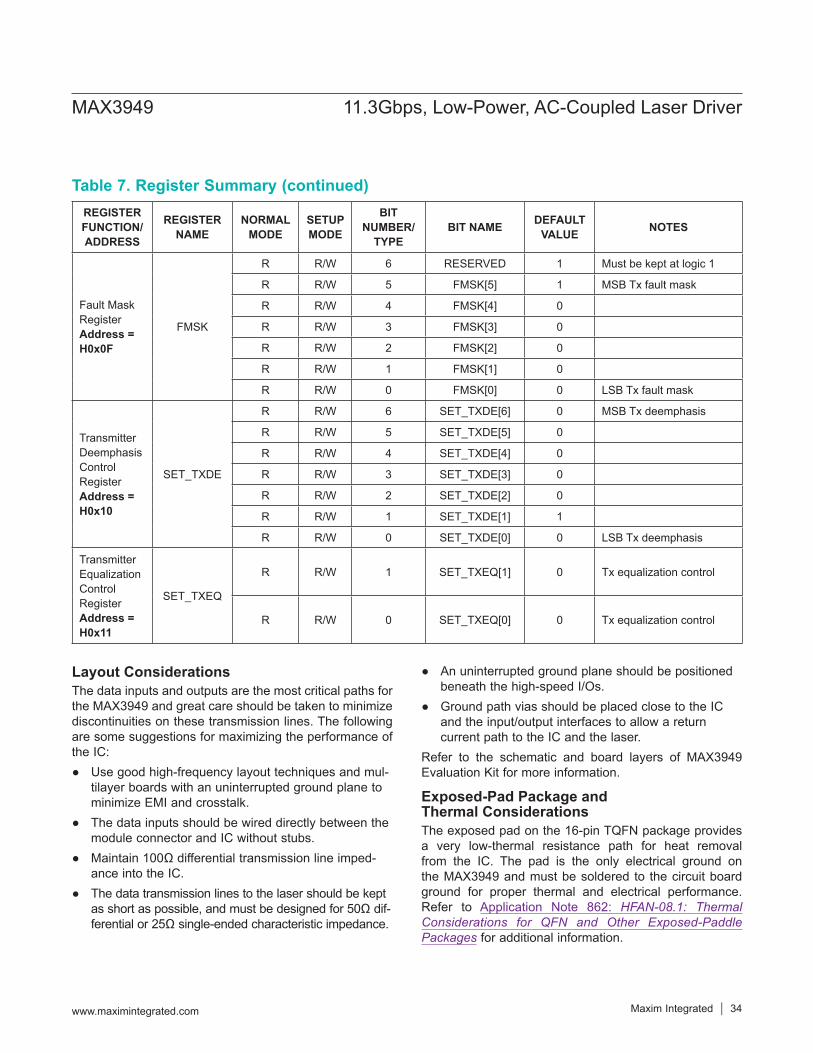
Layout ConsiderationsThe data inputs and outputs are the most critical paths for the MAX3949 and great care should be taken to minimize discontinuities on these transmission lines. The following are some suggestions for maximizing the performance of the IC:
Use good high-frequency layout techniques and mul-tilayer boards with an uninterrupted ground plane to minimize EMI and crosstalk.
The data inputs should be wired directly between the module connector and IC without stubs.
Maintain 100Ω differential transmission line imped-ance into the IC.
The data transmission lines to the laser should be kept as short as possible, and must be designed for 50Ω dif-ferential or 25Ω single-ended characteristic impedance.
An uninterrupted ground plane should be positioned beneath the high-speed I/Os.
Ground path vias should be placed close to the IC and the input/output interfaces to allow a return current path to the IC and the laser.
Refer to the schematic and board layers of MAX3949 Evaluation Kit for more information.
Exposed-Pad Package and Thermal ConsiderationsThe exposed pad on the 16-pin TQFN package provides a very low-thermal resistance path for heat removal from the IC. The pad is the only electrical ground on the MAX3949 and must be soldered to the circuit board ground for proper thermal and electrical performance. Refer to Application Note 862: HFAN-08.1: Thermal Considerations for QFN and Other Exposed-Paddle Packages for additional information.
Table 7. Register Summary (continued)REGISTER FUNCTION/ ADDRESS
REGISTER NAME
NORMAL MODE
SETUP MODE
BIT NUMBER/
TYPEBIT NAME DEFAULT
VALUE NOTES
Fault Mask Register Address = H0x0F
FMSK
R R/W 6 RESERVED 1 Must be kept at logic 1
R R/W 5 FMSK[5] 1 MSB Tx fault mask
R R/W 4 FMSK[4] 0
R R/W 3 FMSK[3] 0
R R/W 2 FMSK[2] 0
R R/W 1 FMSK[1] 0
R R/W 0 FMSK[0] 0 LSB Tx fault mask
Transmitter Deemphasis Control Register Address = H0x10
SET_TXDE
R R/W 6 SET_TXDE[6] 0 MSB Tx deemphasis
R R/W 5 SET_TXDE[5] 0
R R/W 4 SET_TXDE[4] 0
R R/W 3 SET_TXDE[3] 0
R R/W 2 SET_TXDE[2] 0
R R/W 1 SET_TXDE[1] 1
R R/W 0 SET_TXDE[0] 0 LSB Tx deemphasis
Transmitter Equalization Control Register Address = H0x11
SET_TXEQ
R R/W 1 SET_TXEQ[1] 0 Tx equalization control
R R/W 0 SET_TXEQ[0] 0 Tx equalization control
MAX3949 11.3Gbps, Low-Power, AC-Coupled Laser Driver
www.maximintegrated.com Maxim Integrated 34
MAX3949 11.3Gbps, Low-Power, AC-Coupled Laser Driver
www.maximintegrated.com Maxim Integrated 35
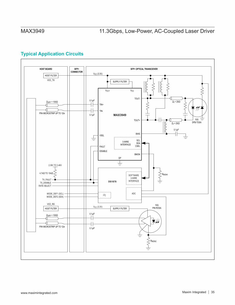
Typical Application Circuits
HOST FILTER
VCC_TX
ZDIFF = 100Ω 0.1µF
0.1µFFR4 MICROSTRIP UP TO 12in
SUPPLY FILTER
VCC (3.3V)
TIN+
TIN-
VSEL
FAULT
DISABLEBMON
TOUT+
BIAS
TOUT-
SCLSDA
CSEL
3-WIREINTERFACE
EP
VCCT VCC
HOST FILTER
VCC_RX
SUPPLY FILTER10G
PIN ROSA
10GDFB-TOSA
SFP+ OPTICAL TRANSCEIVERSFP+CONNECTOR
HOST BOARD
RMON1
RMON2
Z0 = 25Ω
Z0 = 25Ω
ZDIFF = 100Ω 0.1µF
0.1µFFR4 MICROSTRIP UP TO 12in
MAX3949
DS1878
2.38V TO 3.46V
TX_FAULTTX_DISABLE
RATE SELECT
MODE_DEF1 (SCL)
SOFTWARE3-WIRE
INTERFACE
ADCMODE_DEF2 (SDA) I2C
VCC (3.3V)
4.7kΩ TO 10kΩ
0.1µF
MAX3949 11.3Gbps, Low-Power, AC-Coupled Laser Driver
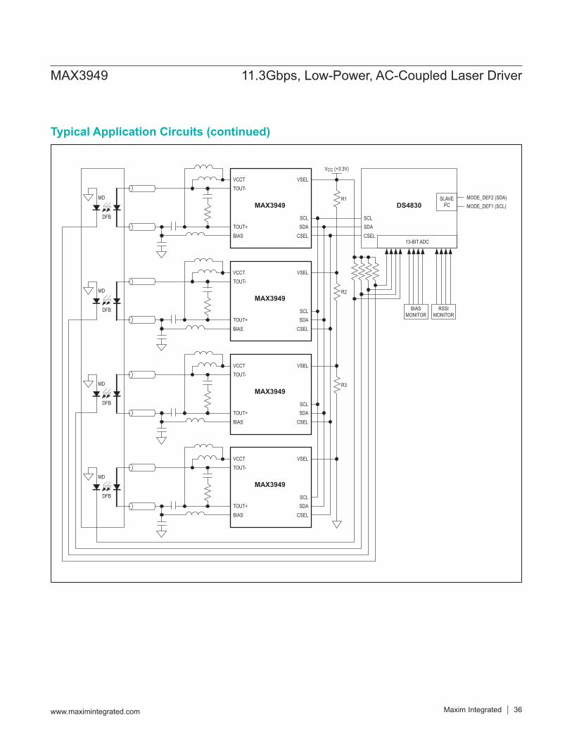
www.maximintegrated.com Maxim Integrated 36
VCCT VSEL
R1
TOUT-
TOUT+BIAS
SDASCL
CSELSDASCL
CSEL13-BIT ADC
SLAVEI2C
BIASMONITOR
MD
DFB
MAX3949 DS4830 MODE_DEF1 (SCL)MODE_DEF2 (SDA)
VCCT VSEL
R2
TOUT-
TOUT+BIAS
SDASCL
CSEL
MD
DFB
MAX3949
VCCT VSEL
R3
TOUT-
TOUT+BIAS
SDASCL
CSEL
MD
DFB
MAX3949
VCCT VSELTOUT-
TOUT+BIAS
SDASCL
CSEL
MD
DFB
MAX3949
VCC (+3.3V)
RSSIMONITOR
Typical Application Circuits (continued)
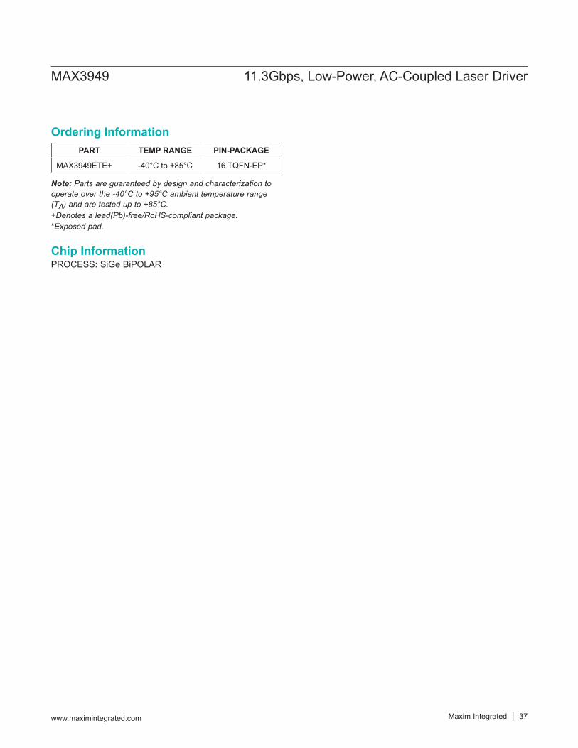
Note: Parts are guaranteed by design and characterization to operate over the -40°C to +95°C ambient temperature range (TA) and are tested up to +85°C.+Denotes a lead(Pb)-free/RoHS-compliant package.*Exposed pad.
PART TEMP RANGE PIN-PACKAGE
MAX3949ETE+ -40°C to +85°C 16 TQFN-EP*
MAX3949 11.3Gbps, Low-Power, AC-Coupled Laser Driver
www.maximintegrated.com Maxim Integrated 37
Chip InformationPROCESS: SiGe BiPOLAR
Ordering Information
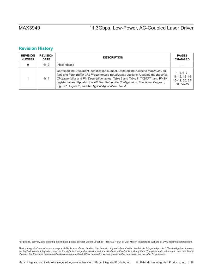
REVISION NUMBER
REVISION DATE DESCRIPTION PAGES
CHANGED
0 6/12 Initial release —
1 4/14
Corrected the Document Identification number. Updated the Absolute Maximum Rat-ings and Input Buffer with Progammable Equalization sections. Updated the Electrical Characteristics and Pin Description tables, Table 3 and Table 7, TXSTAT1 and FMSK register tables. Updated the AC Test Setup, Pin Configuration, Functional Diagram, Figure 1, Figure 2, and the Typical Application Circuit.
1–4, 6–7, 11–12, 15–16 18–19, 23, 27
30, 34–35
Maxim Integrated cannot assume responsibility for use of any circuitry other than circuitry entirely embodied in a Maxim Integrated product. No circuit patent licenses are implied. Maxim Integrated reserves the right to change the circuitry and specifications without notice at any time. The parametric values (min and max limits) shown in the Electrical Characteristics table are guaranteed. Other parametric values quoted in this data sheet are provided for guidance.
Maxim Integrated and the Maxim Integrated logo are trademarks of Maxim Integrated Products, Inc.
MAX3949 11.3Gbps, Low-Power, AC-Coupled Laser Driver
© 2014 Maxim Integrated Products, Inc. 38
Revision History
For pricing, delivery, and ordering information, please contact Maxim Direct at 1-888-629-4642, or visit Maxim Integrated’s website at www.maximintegrated.com.