LT3688 - Dual 800mA Step-Down Switching Regulator with ...€¦ · Watchdog Timer The LT ... n...
28
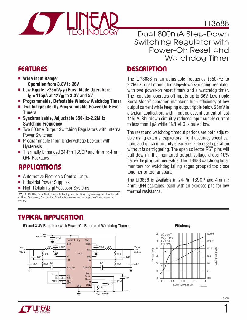
LT3688 1 3688f TYPICAL APPLICATION FEATURES APPLICATIONS DESCRIPTION Dual 800mA Step-Down Switching Regulator with Power-On Reset and Watchdog Timer The LT ® 3688 is an adjustable frequency (350kHz to 2.2MHz) dual monolithic step-down switching regulator with two power-on reset timers and a watchdog timer. The regulator operates off inputs up to 36V. Low ripple Burst Mode ® operation maintains high efficiency at low output current while keeping output ripple below 25mV in a typical application, with input quiescent current of just 115μA. Shutdown circuitry reduces input supply current to less than 1μA while EN/UVLO is pulled low. The reset and watchdog timeout periods are both adjust- able using external capacitors. Tight accuracy specifica- tions and glitch immunity ensure reliable reset operation without false triggering. The open collector RST pins will pull down if the monitored output voltage drops 10% below the programmed value. The LT3688 watchdog timer monitors for watchdog falling edges grouped too close together or too far apart. The LT3688 is available in 24-Pin TSSOP and 4mm × 4mm QFN packages, each with an exposed pad for low thermal resistance. 5V and 3.3V Regulator with Power-On Reset and Watchdog Timers n Wide Input Range: Operation from 3.8V to 36V n Low Ripple (<25mV P-P ) Burst Mode Operation: I Q = 115μA at 12V IN to 3.3V and 5V n Programmable, Defeatable Window Watchdog Timer n Two Independently Programmable Power-On-Reset Timers n Synchronizable, Adjustable 350kHz-2.2MHz Switching Frequency n Two 800mA Output Switching Regulators with Internal Power Switches n Programmable Input Undervoltage Lockout with Hysteresis n Thermally Enhanced 24-Pin TSSOP and 4mm × 4mm QFN Packages n Automotive Electronic Control Units n Industrial Power Supplies n High-Reliability μProcessor Systems EN/UVLO V IN LT3688 GND BIAS BST1 0.22μF 4.7μF V OUT1 5V 800mA V IN 6V TO 36V 22μF 22pF 18μH 12μH 523k 100k 316k 100k 1nF 1nF μP 0.22μF SW1 DA1 BST2 SW2 DA2 FB1 RUN/SS1 WDI WDO RST1 RST2 I/O I/O RESET FB2 RUN/SS2 C WDT C POR1 C POR2 RT SYNC 22μF 1nF 3688 TA01a 4.7nF 4.7nF 110k f SW = 500kHz V OUT2 3.3V 800mA 22pF Efficiency 3688 TA01b 0.0001 1 0.001 0.01 0.1 LOAD CURRENT (A) EFFICIENCY (%) 60 70 80 50 30 40 90 POWER LOSS (mW) 10.0 100.0 1000.0 1.0 0.01 0.1 10000.0 V IN = 12V V OUT = 3.3V L = 4.7μH f = 800kHz L, LT, LTC, LTM, Burst Mode, Linear Technology and the Linear logo are registered trademarks of Linear Technology Corporation. All other trademarks are the property of their respective owners.
-
Upload
nguyenmien -
Category
Documents
-
view
214 -
download
0
Transcript of LT3688 - Dual 800mA Step-Down Switching Regulator with ...€¦ · Watchdog Timer The LT ... n...
LT3688
13688f
TYPICAL APPLICATION
FEATURES
APPLICATIONS
DESCRIPTION
Dual 800mA Step-Down Switching Regulator with
Power-On Reset and Watchdog Timer
The LT®3688 is an adjustable frequency (350kHz to 2.2MHz) dual monolithic step-down switching regulator with two power-on reset timers and a watchdog timer. The regulator operates off inputs up to 36V. Low ripple Burst Mode® operation maintains high effi ciency at low output current while keeping output ripple below 25mV in a typical application, with input quiescent current of just 115μA. Shutdown circuitry reduces input supply current to less than 1μA while EN/UVLO is pulled low.
The reset and watchdog timeout periods are both adjust-able using external capacitors. Tight accuracy specifi ca-tions and glitch immunity ensure reliable reset operation without false triggering. The open collector RST pins will pull down if the monitored output voltage drops 10% below the programmed value. The LT3688 watchdog timer monitors for watchdog falling edges grouped too close together or too far apart.
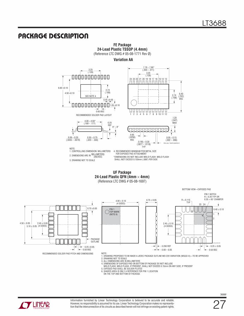
The LT3688 is available in 24-Pin TSSOP and 4mm × 4mm QFN packages, each with an exposed pad for low thermal resistance.
5V and 3.3V Regulator with Power-On Reset and Watchdog Timers
n Wide Input Range: Operation from 3.8V to 36Vn Low Ripple (<25mVP-P ) Burst Mode Operation:
IQ = 115μA at 12VIN to 3.3V and 5Vn Programmable, Defeatable Window Watchdog Timern Two Independently Programmable Power-On-Reset
Timersn Synchronizable, Adjustable 350kHz-2.2MHz
Switching Frequencyn Two 800mA Output Switching Regulators with Internal
Power Switchesn Programmable Input Undervoltage Lockout with
Hysteresisn Thermally Enhanced 24-Pin TSSOP and 4mm × 4mm
QFN Packages
n Automotive Electronic Control Unitsn Industrial Power Suppliesn High-Reliability μProcessor Systems
EN/UVLO VIN
LT3688
GND
BIAS
BST10.22μF
4.7μF
VOUT15V
800mA
VIN6V TO 36V
22μF
22pF
18μH 12μH
523k
100k
316k
100k1nF 1nF
μP
0.22μF
SW1
DA1
BST2
SW2
DA2
FB1
RUN/SS1
WDIWDO
RST1
RST2
I/OI/O
RESET
FB2
RUN/SS2
CWDT
CPOR1
CPOR2
RTSYNC
22μF
1nF
3688 TA01a
4.7nF
4.7nF
110k
fSW = 500kHz
VOUT23.3V800mA
22pF
Effi ciency
3688 TA01b
0.0001 10.001 0.01 0.1
LOAD CURRENT (A)
EFF
ICIE
NC
Y (
%)
60
70
80
50
30
40
90
PO
WE
R L
OS
S (m
W)
10.0
100.0
1000.0
1.0
0.01
0.1
10000.0VIN = 12VVOUT = 3.3VL = 4.7μHf = 800kHz
L, LT, LTC, LTM, Burst Mode, Linear Technology and the Linear logo are registered trademarks of Linear Technology Corporation. All other trademarks are the property of their respective owners.
LT3688
23688f
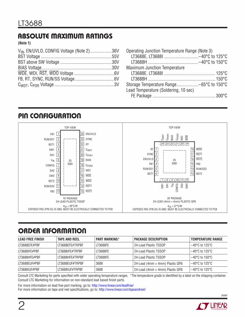
ABSOLUTE MAXIMUM RATINGS
VIN, EN/UVLO, CONFIG Voltage (Note 2) ...................36VBST Voltage ..............................................................55VBST above SW Voltage .............................................30VBIAS Voltage .............................................................30VWDE, WDI, RST, WDO Voltage ...................................6VFB, RT , SYNC, RUN/SS Voltage ..................................6VCWDT , CPOR Voltage ....................................................3V
1
2
3
4
5
6
7
8
9
10
11
12
TOP VIEW
FE PACKAGE24-LEAD PLASTIC TSSOP
24
23
22
21
20
19
18
17
16
15
14
13
FB1
RUN/SS1
BST1
SW1
DA1
VIN
CONFIG
DA2
SW2
BST2
RUN/SS2
FB2
EN/UVLO
SYNC
RT
CWDT
CPOR1
BIAS
CPOR2
WDI
WDE
WDO
RST1
RST2
25GND
θJA = 38°C/WEXPOSED PAD (PIN 25) IS GND, MUST BE ELECTRICALLY CONNECTED TO PCB
24 23 22 21 20 19
7 8 9
TOP VIEW
UF PACKAGE24-LEAD (4mm × 4mm) PLASTIC QFN
10 11 12
6
5
4
3
2
1
13
14
15
16
17
18RT
SYNC
EN/UVLO
FB1
RUN/SS1
BST1
WDO
RST1
RST2
FB2
RUN/SS2
BST2
CW
DT
CP
OR
1
BIA
S
CP
OR
2
WD
I
WD
E
SW
1
DA
1
VIN
CO
NFI
G
DA
2
SW
2
25
GND
θJA = 37°C/WEXPOSED PAD (PIN 25) IS GND, MUST BE ELECTRICALLY CONNECTED TO PCB
PIN CONFIGURATION
ORDER INFORMATIONLEAD FREE FINISH TAPE AND REEL PART MARKING* PACKAGE DESCRIPTION TEMPERATURE RANGE
LT3688EFE#PBF LT3688EFE#TRPBF LT3688FE 24-Lead Plastic TSSOP –40°C to 125°C
LT3688IFE#PBF LT3688IFE#TRPBF LT3688FE 24-Lead Plastic TSSOP –40°C to 125°C
LT3688HFE#PBF LT3688HFE#TRPBF LT3688FE 24-Lead Plastic TSSOP –40°C to 150°C
LT3688EUF#PBF LT3688EUF#TRPBF 3688 24-Lead (4mm × 4mm) Plastic QFN –40°C to 125°C
LT3688IUF#PBF LT3688IUF#TRPBF 3688 24-Lead (4mm × 4mm) Plastic QFN –40°C to 125°C
Consult LTC Marketing for parts specifi ed with wider operating temperature ranges. *The temperature grade is identifi ed by a label on the shipping container.
Consult LTC Marketing for information on non-standard lead based fi nish parts.
For more information on lead free part marking, go to: http://www.linear.com/leadfree/ For more information on tape and reel specifi cations, go to: http://www.linear.com/tapeandreel/
(Note 1)
Operating Junction Temperature Range (Note 3) LT3688E, LT3688I ..............................–40°C to 125°C LT3688H ............................................–40°C to 150°CMaximum Junction Temperature LT3688E, LT3688I ............................................. 125°C LT3688H ........................................................... 150°CStorage Temperature Range ...................–65°C to 150°CLead Temperature (Soldering, 10 sec) FE Package ....................................................... 300°C
LT3688
33688f
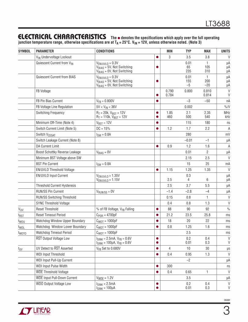
The l denotes the specifi cations which apply over the full operating junction temperature range, otherwise specifi cations are at TA = 25°C. VIN = 12V, unless otherwise noted. (Note 3) ELECTRICAL CHARACTERISTICS
SYMBOL PARAMETER CONDITIONS MIN TYP MAX UNITS
VIN Undervoltage Lockout l 3 3.5 3.8 V
Quiescent Current from VIN VEN/UVLO = 0.3VVBIAS = 5V, Not SwitchingVBIAS = 0V, Not Switching
l
0.0165
235
1105310
μAμAμA
Quiescent Current from BIAS VEN/UVLO = 0.3VVBIAS = 5V, Not SwitchingVBIAS = 0V, Not Switching
l
0.01155–5
1200–20
μAμAμA
FB Voltage l
0.7900.784
0.800 0.8100.814
VV
FB Pin Bias Current VFB = 0.800V l –3 –50 nA
FB Voltage Line Regulation 5V < VIN < 36V 0.002 %/V
Switching Frequency RT = 20k, VBST = 12VRT = 110k, VBST = 12V
l
l
1.85460
2.1500
2.35540
MHzkHz
Minimum Off-Time (Note 4) VBST = 12V l 115 180 ns
Switch Current Limit (Note 5) DC = 15% l 1.2 1.7 2.2 A
Switch VCESAT ISW = 0.8A 280 mV
Switch Leakage Current (Note 8) –0.01 –1 μA
DA Current Limit l 0.9 1.2 1.6 A
Boost Schottky Reverse Leakage VBIAS = 0V 0.01 2 μA
Minimum BST Voltage above SW 2.15 2.5 V
BST Pin Current ISW = 0.8A 15 25 mA
EN/UVLO Threshold Voltage l 1.15 1.25 1.35 V
EN/UVLO Input Current VEN/UVLO = 1.35VVEN/UVLO = 1.15V 2.5
0.34 6
μAμA
Threshold Current Hysteresis 2.5 3.7 5.5 μA
RUN/SS Pin Current VRUN/SS = 0V –1.4 –2.8 –4 μA
RUN/SS Switching Threshold 0.15 0.8 1 V
SYNC Threshold Voltage 0.4 0.8 1.3 V
VUV Reset Threshold % of FB Voltage, VFB Falling l 88 90 92 %
tRST Reset Timeout Period CPOR = 4700pF l 21.2 23.5 25.8 ms
tWDU Watchdog Window Upper Boundary CWDT = 1000pF l 18 20 22 ms
tWDL Watchdog Window Lower Boundary CWDT = 1000pF l 0.8 1.25 1.6 ms
tWDTO Watchdog Timeout Period CWDT = 1000pF 2.5 ms
RST Output Voltage Low ISINK = 2.5mA, VFB = 0.6VISINK = 100μA, VFB = 0.6V
l
l
0.20.01
0.40.3
VV
tUV UV Detect to RST Asserted VFB Set to 0.680V l 4 10 30 μs
WDI Input Threshold l 0.4 0.95 1.3 V
WDI Input Pull-Up Current –2 μA
WDI Input Pulse Width l 300 ns
WDE Threshold Voltage l 0.4 0.65 1 V
WDE Input Pull-Down Current VWDE = 1.2V 3.5 μA
WDO Output Voltage Low ISINK = 2.5mAISINK = 100μA
l
l
0.20.01
0.40.3
VV
LT3688
43688f
The l denotes the specifi cations which apply over the full operating junction temperature range, otherwise specifi cations are at TA = 25°C. VIN = 12V, unless otherwise noted. (Note 3)
SYMBOL PARAMETER CONDITIONS MIN TYP MAX UNITS
RST Pull-Up Current (Note 6) –1.5 –2.5 μA
WDO Pull-Up Current (Note 6) –1.5 –2.5 μA
CONFIG Low Level Input Voltage l 0.2 V
CONFIG High Level Input Voltage l 1.4 V
CONFIG Pin Voltage When Open 0.64 V
Maximum CONFIG Input Current in Open State
l ±1 μA
CONFIG Pin Bias Current VCONFIG = 0V, VIN l ±20 μA
ELECTRICAL CHARACTERISTICS
Note 1: Stresses beyond those listed under Absolute Maximum Ratings
may cause permanent damage to the device. Exposure to any Absolute
Maximum Rating condition for extended periods may affect device
reliability and lifetime.
Note 2: Absolute Maximum Voltage at the VIN, CONFIG and EN/UVLO pins
is 36V for continuous operation.
Note 3: The LT3688 is tested under pulsed load conditions such that
TJ = TA. The LT3688E is guaranteed to meet performance specifi cations
from 0°C to 125°C junction temperature. Specifi cations over the –40°C
to 125°C operating junction temperature range are assured by design,
characterization and correlation with statistical process controls. The
LT3688I is guaranteed over the full –40°C to 125°C operating junction
temperature range. The LT3688H is guaranteed over the full –40°C to
150°C operating junction temperature range. High junction temperatures
degrade operating lifetimes. Operating lifetime is derated at junction
temperatures greater than 125°C. The junction temperature (TJ, in °C) is
calculated from the ambient temperature (TA, in °C) and power dissipation
(PD, in Watts) according to the formula:
TJ = TA + (PD θJA), where θJA (in °C/W) is the package thermal
impedance.
Note 4: The LT3688 contains circuitry that extends the maximum duty
cycle if the BST voltage is 2V greater than the SW voltage. See the
Applications Information section for more details.
Note 5: Current limit is guaranteed by design and/or correlation to static
test. Slope compensation reduces current limit at higher duty cycles.
Note 6: The outputs of RST and WDO have a weak pull-up to VBIAS of
typically 2.5μA. However, external pull-up resistors may be used when
faster rise times are required or for VOH higher than VBIAS.
Note 7: This IC includes overtemperature protection that is intended
to protect the device during momentary overload conditions. Junction
temperature will exceed the maximum operating junction temperature
when over-temperature protection is active. Continuous operation above
the specifi ed maximum operating junction temperature may impair device
reliability.
Note 8: All currents into pins are positive; all voltages are referenced to
GND unless otherwise specifi ed.
TYPICAL PERFORMANCE CHARACTERISTICSEffi ciency, VOUT = 5V Effi ciency, VOUT = 3.3V Effi ciency, VOUT = 1.8V
TA = 25°C unless otherwise noted.
LOAD CURRENT (A)
0 0.2 0.4 0.6 0.8 165
EFF
ICIE
NC
Y (
%) 85
90
80
70
75
95
3688 G01
fSW = 1MHzVIN = 12V
LOAD CURRENT (A)
0 0.2 0.4 0.6 0.8 160
EFF
ICIE
NC
Y (
%) 80
85
75
65
70
90
3688 G02
fSW = 1MHzVIN = 12V
LOAD CURRENT (A)
0 0.2 0.4 0.6 0.8 155
EFF
ICIE
NC
Y (
%) 75
80
70
60
65
85
3688 G03
fSW = 500kHzVIN = 12V
LT3688
53688f
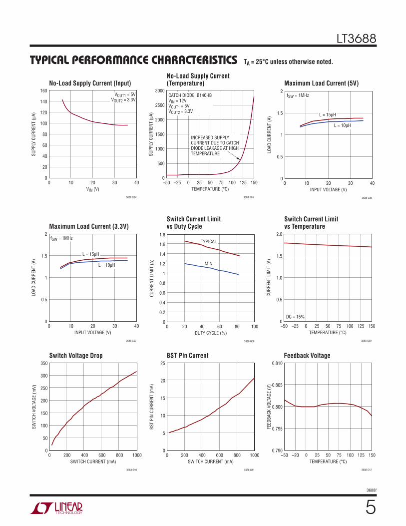
TYPICAL PERFORMANCE CHARACTERISTICS
No-Load Supply Current (Input)No-Load Supply Current (Temperature) Maximum Load Current (5V)
Maximum Load Current (3.3V)Switch Current Limit vs Duty Cycle
Switch Current Limit vs Temperature
TA = 25°C unless otherwise noted.
VIN (V)
0 10 20 30 400
SU
PP
LY C
UR
REN
T (
μA
) 120
140
100
40
60
20
80
160
3688 G04
VOUT1 = 5VVOUT2 = 3.3V
INPUT VOLTAGE (V)
0 10 20 30 400
LO
AD
CU
RR
EN
T (
A)
1.5
0.5
1
2
3688 G06
L = 15μH
L = 10μH
fSW = 1MHz
INPUT VOLTAGE (V)
fSW = 1MHz
0 10 20 30 400
LO
AD
CU
RR
EN
T (
A)
1.5
0.5
1
2
3688 G07
L = 15μH
L = 10μH
DUTY CYCLE (%)
0 20 40 60 80 1000
CU
RR
EN
T L
IMIT
(A
)
1.4
0.2
0.4
0.6
1
1.2
1.6
0.8
1.8
3688 G08
TYPICAL
MIN
TEMPERATURE (°C)
–50 –25 0 50 7525 100 125 1500
CU
RR
EN
T L
IMIT
(A
)
0.5
1.0
1.5
2.0
3688 G09
DC = 15%
Switch Voltage Drop BST Pin Current Feedback Voltage
SWITCH CURRENT (mA)
0 200 400 800600 10000
SW
ITC
H V
OLT
AG
E (
mV
)
50
100
150
250
300
200
350
3688 G10
SWITCH CURRENT (mA)
0 200 400 800600 10000
BS
T P
IN C
UR
REN
T (
mA
)
5
15
20
10
25
3688 G11
TEMPERATURE (°C)
–50 –20 25 500 100 12575 1500.790
FEED
BA
CK
VO
LTA
GE (
V)
0.795
0.805
0.800
0.810
3688 G12
TEMPERATURE (°C)
–50 –25 0 25 50 75 100 125 1500
SU
PP
LY C
UR
REN
T (
μA
)
2500
1000
1500
500
2000
3000
3688 G05
CATCH DIODE: B140HBVIN = 12VVOUT1 = 5VVOUT2 = 3.3V
INCREASED SUPPLY CURRENT DUE TO CATCH DIODE LEAKAGE AT HIGH TEMPERATURE
LT3688
63688f
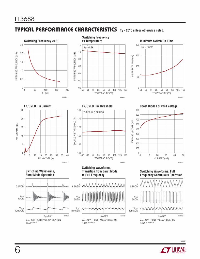
TYPICAL PERFORMANCE CHARACTERISTICS
Switching Frequency vs RT
Switching Frequency vs Temperature Minimum Switch On-Time
EN/UVLO Pin Current EN/UVLO Pin Threshold Boost Diode Forward Voltage
Switching Waveforms, Burst Mode Operation
Switching Waveforms, Transition from Burst Mode to Full Frequency
Switching Waveforms, Full Frequency Continuous Operation
TA = 25°C unless otherwise noted.
TEMPERATURE (°C)
RT = 49.9k
–50 –25 25 500 100 12575 1500.0
SW
ITC
HIN
G F
REQ
UEN
CY
(M
Hz)
0.2
0.8
0.6
0.4
1.2
1.0
3688 G14
TEMPERATURE (°C)
ISW = 700mA
–50 –20 25 500 100 12575 1500
MIN
IMU
M O
N T
IME (
ns)
50
150
100
200
3688 G16
PIN VOLTAGE (V)
0 5 15 2010 30 3525 400
PIN
CU
RR
EN
T (
μA
)
5
15
20
10
25
3688 G17
TEMPERATURE (°C)
THRESHOLD FALLING
–50 –25 25 500 100 12575 1501.00
EN
/UV
LO
PIN
TH
RES
HO
LD
(V
)
1.10
1.30
1.40
1.20
1.50
3688 G18
CURRENT (mA)
0 10 20 30 40 500
FOR
WA
RD
VO
LTA
GE (
mV
)
100
500
600
700
800
200
300
400
900
3688 G19
IL0.2A/DIV
VIN = 12V; FRONT PAGE APPLICATIONILOAD = 40mA
VSW5V/DIV
VOUT10mV/DIV
5μs/DIV 3688 G21
IL0.2A/DIV
VIN = 12V; FRONT PAGE APPLICATIONILOAD = 160mA
VSW5V/DIV
VOUT10mV/DIV
5μs/DIV 3688 G22
RT (kΩ)
0 10050 150 2000
SW
ITC
HIN
G F
REQ
UEN
CY
(M
Hz)
0.5
1.5
2.0
1.0
2.5
3688 G13
IL0.2A/DIV
VIN = 12V; FRONT PAGE APPLICATIONILOAD = 7mA
VSW5V/DIV
VOUT10mV/DIV
5μs/DIV 3688 G20
LT3688
73688f
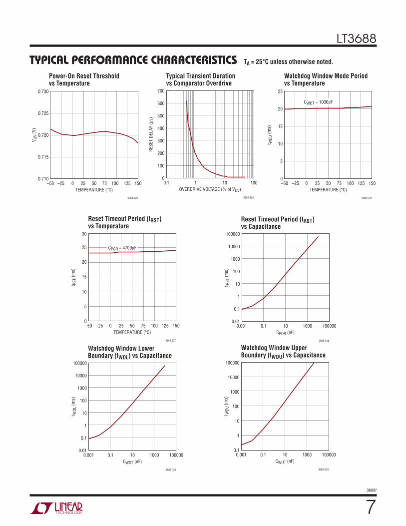
TYPICAL PERFORMANCE CHARACTERISTICSPower-On Reset Threshold vs Temperature
Typical Transient Duration vs Comparator Overdrive
Watchdog Window Mode Period vs Temperature
Reset Timeout Period (tRST)vs Temperature
TA = 25°C unless otherwise noted.
TEMPERATURE (°C)
–50 –25 0 25 50 75 100 125 1500.710
VU
V (
V)
0.725
0.715
0.720
0.730
3688 G23
OVERDRIVE VOLTAGE (% of VUV)
0.1 1 10 1000
RES
ET D
ELA
Y (
μs)
600
100
200
300
400
500
700
3688 G24
TEMPERATURE (°C)
CWDT = 1000pF
–50 –25 0 25 50 75 100 125 1500
t WD
U (
ms)
5
10
15
20
25
3688 G26
TEMPERATURE (°C)
CPOR = 4700pF
–50 –25 0 25 50 75 100 125 1500
t RS
T (
ms)
5
10
15
20
25
30
3688 G27
Reset Timeout Period (tRST) vs Capacitance
CPOR (nF)
0.001 0.1 10 1000 1000000.01
t RS
T (
ms)
0.1
10
100
1000
10000
1
100000
3688 G28
Watchdog Window Lower Boundary (tWDL) vs Capacitance
Watchdog Window Upper Boundary (tWDU) vs Capacitance
CWDT (nF)
0.001 0.1 10 1000 1000000.01
t WD
L (
ms)
0.1
10
100
1000
10000
1
100000
3688 G29
CWDT (nF)
0.001 0.1 10 1000 1000000.1
t WD
U (
ms)
1
10
100
1000
10000
100000
3688 G30
LT3688
83688f
RT (Pin 1/Pin 22): The RT pin is used to set the internal oscillator frequency. Tie a resistor from RT to GND to set the switching frequency.
SYNC (Pin 2/Pin 23): Drive the SYNC pin with a logic-level signal with positive and negative pulse widths of at least 150ns. Do not fl oat this pin. Tie to GND if the SYNC feature is not used.
EN/UVLO (Pin 3/Pin 24): The EN/UVLO pin is used to put the LT3688 in shutdown mode. Pull the pin below 0.3V to shut down the LT3688. The 1.25V threshold can function as an accurate undervoltage lockout (UVLO), preventing the regulator from operating until the input voltage has reached the programmed level.
FB1, FB2 (Pins 4, 15/Pins 1, 12): The LT3688 regulates the feedback pins to 0.800V. Connect the feedback resistor divider taps to this pin.
RUN/SS1, RUN/SS2 (Pins 5, 14/Pins 2, 11): Place a capacitor from RUN/SS to GND to program the soft start period. Use a 1000pF or larger capacitor at these pins. To ensure the SS capacitors are discharged, internal circuitry pulls the RUN/SS pins low and disables switching during startup before initiating the soft-start sequence. Once the RUN/SS pins fall below 0.2V, the pull down turns off, the SS capacitors start charging again, and switching is enabled. Do not drive these pins directly. Use an open drain or collector to pull them low, if necessary.
BST1, BST2 (Pins 6, 13/Pins 3, 10): The BST pins are used to provide drive voltage, higher than the input volt-age, to the internal NPN power switches.
SW1, SW2 (Pins 7, 12/Pins 4, 9): The SW pins are the outputs of the internal power switches. Connect these pins to the inductors, catch diodes and boost capacitors.
DA1, DA2 (Pins 8, 11/Pins 5, 8): Tie the DA pin to the anode of the external catch Schottky diode. If the DA pin current exceeds 1.2A, which could occur in an overload or short-circuit condition, switching is disabled until the DA pin current falls below 1.2A.
VIN (Pin 9/Pin 6): The VIN pin supplies current to the LT3688’s internal circuitry and to the internal power switches and must be locally bypassed.
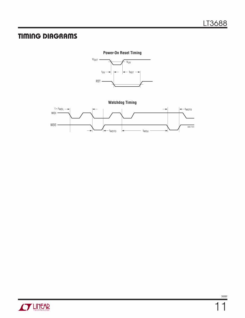
PIN FUNCTIONSCONFIG (Pin 10/Pin 7): The CONFIG pin programs the start-up sequence of the two voltage regulators and the behavior of the power-on reset and watchdog timers. To select one of three confi guration options, tie the CONFIG pin to VIN, tie the CONFIG pin to GND or leave the CONFIG pin fl oating. With the CONFIG pin tied to VIN, each reset output depends on its respective FB pin. Channel 2 only starts when FB1 rises above 0.72V, and the watchdog timer only starts when both RST pins go high. With the CONFIG pin tied to GND, both RST pins pull low until both FB pins rise above 0.72V and the POR timer programmed by CPOR1 expires. Again, channel 2 only starts when FB1 rises above 0.72V, and the watchdog timer only starts when both RST pins go high. Tie CPOR2 to GND if the CONFIG pin is tied low. With the CONFIG pin fl oating, both channels start coincidentally, each reset output depends on its respective FB pin, and the watchdog timer starts when RST1 goes high.
RST1, RST2 (Pins 17, 16/Pins 14, 13): The RST pins are active low, open-drain logic outputs with a weak pull-up to BIAS. After VFB rises above 0.72V, the reset remains asserted for the period set by the capacitor on the CPOR pin. Tie the RST pins to BIAS with a 100k resistor for a stronger pull-up.
WDO (Pin 18/Pin 15): WDO will go low if the micropro-cessor fails to drive the WDI pin of the LT3688 with the appropriate signal. Tie the WDO pin to BIAS with a 100k resistor for a stronger pull-up. Keep capacitive loading on this pin below 1000pF.
WDE (Pin 19/Pin 16): The watchdog timer enable pin disables the watchdog timer if the WDE voltage exceeds 1V. Float this pin or tie to ground for normal operation.
WDI (Pin 20/Pin 17): The watchdog timer input pin receives the watchdog signal from the microprocessor. If two or more negative edges occur on WDI before the programmed fast timer period or no negative edge occurs within the slow timer period, the part will pulse WDO low with a pulse width of 1/8th of the slow timer period. Drive the WDI pin with a pulse width of at least 300ns.
BIAS (Pin 22/Pin 19): The BIAS pin supplies current to the internal circuitry when BIAS is above 3V, helping reduce input quiescent current. The internal Schottky diodes are connected from BIAS to BST, providing the charging path for the boost capacitors.
(QFN/TSSOP)
LT3688
93688f
PIN FUNCTIONS (QFN/TSSOP)
CPOR1, CPOR2 (Pins 23, 21/Pins 20, 18): Place a capacitor between this pin and ground to set the power-on-reset timeout period.
CWDT (Pin 24/Pin 21): Place a capacitor between this pin and ground to set the fast and slow watchdog timer periods.
Exposed Pad (Pin 25/Pin 25): Ground. Tie the exposed pad directly to the ground plane. The exposed pad metal of the package provides both electrical contact to ground and good thermal contact to the printed circuit board. The device must be soldered to the circuit board for proper operation.
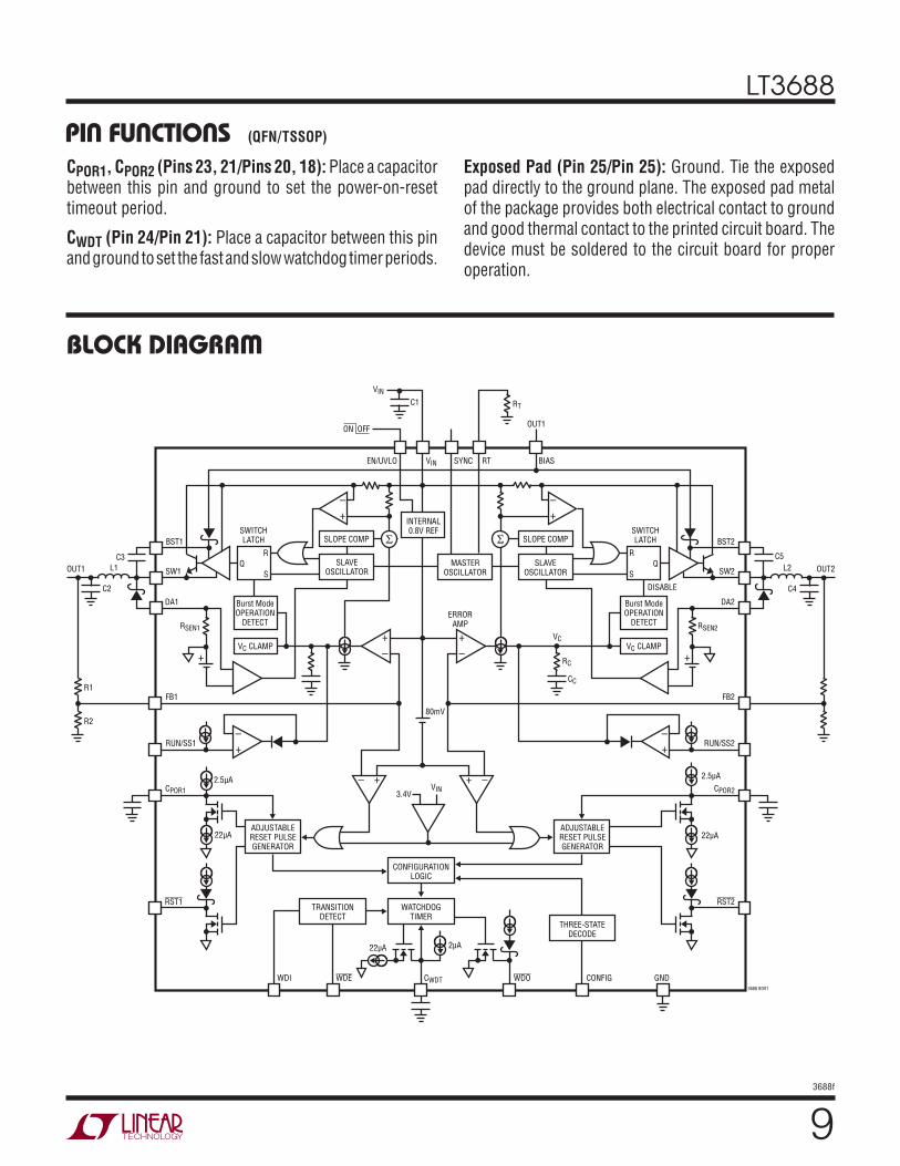
BLOCK DIAGRAM
+
–
+ –
+
– +
BST2
SW2
DA2
RSEN2
DISABLE
Q
S
R
RT
RT
SLAVEOSCILLATOR
MASTEROSCILLATOR
INTERNAL0.8V REF
ERRORAMP
SLOPE COMPSWITCHLATCH
Burst ModeOPERATION
DETECT
ADJUSTABLERESET PULSEGENERATOR
VC CLAMP
C5
CC
VIN3.4V
RC
VC
C4
OUT2L2
FB2
RUN/SS2
CPOR2
2.5μA
22μA
3688 BD01
RST2
BIAS
OUT1
SYNCVIN
VIN
EN/UVLO
ON OFF
+
–
+–
+
–+
BST1
SW1
DA1
RSEN1
Q
S
RSLAVE
OSCILLATOR
CONFIGURATIONLOGIC
WATCHDOGTIMER
TRANSITIONDETECT
SLOPE COMPSWITCHLATCH
Burst ModeOPERATION
DETECT
ADJUSTABLERESET PULSEGENERATOR
VC CLAMP
OUT1
FB1
R2
R1
C2
C3
L1
RUN/SS1
CPOR1
2.5μA
2μA22μA
22μA
RST1
CWDTWDEWDI WDO CONFIG GND
THREE-STATEDECODE
+
–
+
–
80mV
C1
LT3688
103688f
OPERATIONThe LT3688 is a constant-frequency, current mode step-down regulator with two reset timers and a watchdog timer that perform microprocessor supervisory functions. Operation can be best understood by referring to the Block Diagram. Keeping the EN/UVLO pin at ground completely shuts off the part drawing minimal current from the VIN source. To turn on the internal bandgap and the rest of the logic circuitry, raise the EN/UVLO pin above the accurate threshold of 1.25V. Also, VIN needs to be higher than 3.5V for the part to start switching.
Switching Regulator Operation
An oscillator, with frequency set by RT, enables an RS fl ip fl op, turning on the internal power switch. An amplifi er and comparator monitor the current fl owing between the VIN and SW pins, turning the switch off when this cur-rent reaches a level determined by the voltage at VC. An error amplifi er measures the output voltage through an external resistor divider tied to the FB pin and servos the VC voltage. If the error amplifi er’s output increases, more current is delivered to the output; if it decreases, less current is delivered. An active clamp on the VC voltage provides current limit. The VC voltage is also controlled by the internal soft-start circuit during start-up or after a fault condition takes place.
An internal regulator provides power to the control cir-cuitry. The internal regulator normally draws current from the VIN pin, but if the BIAS pin is connected to an external voltage higher than 3V, bias current will be drawn from the external source (typically the regulated output voltage). This improves effi ciency. The BIAS pin also provides a current path to the internal boost diode that charges up the boost capacitor. The switch driver operates either from the VIN or from the BST pin. An external capacitor is used to generate a voltage at the BST pin that is higher than the VIN supply. This allows the driver to fully saturate the internal NPN power switch for effi cient operation. To further
optimize effi ciency, the LT3688 automatically switches to Burst Mode operation in light load situations. Between bursts, all circuitry associated with controlling the output switch is shut down, reducing the input supply current to 115μA in a typical application.
A comparator monitors the current fl owing through the catch diode via the DA pin. This comparator delays switch-ing if the diode current goes higher than 1.2A (typical) during a fault condition such as a shorted output with high input voltage. Switching will only resume once the diode current has fallen below the 1.2A limit. This way the DA comparator regulates the valley current of the inductor to 1.2A during short circuit. This will ensure that the part will survive a short-circuit event.
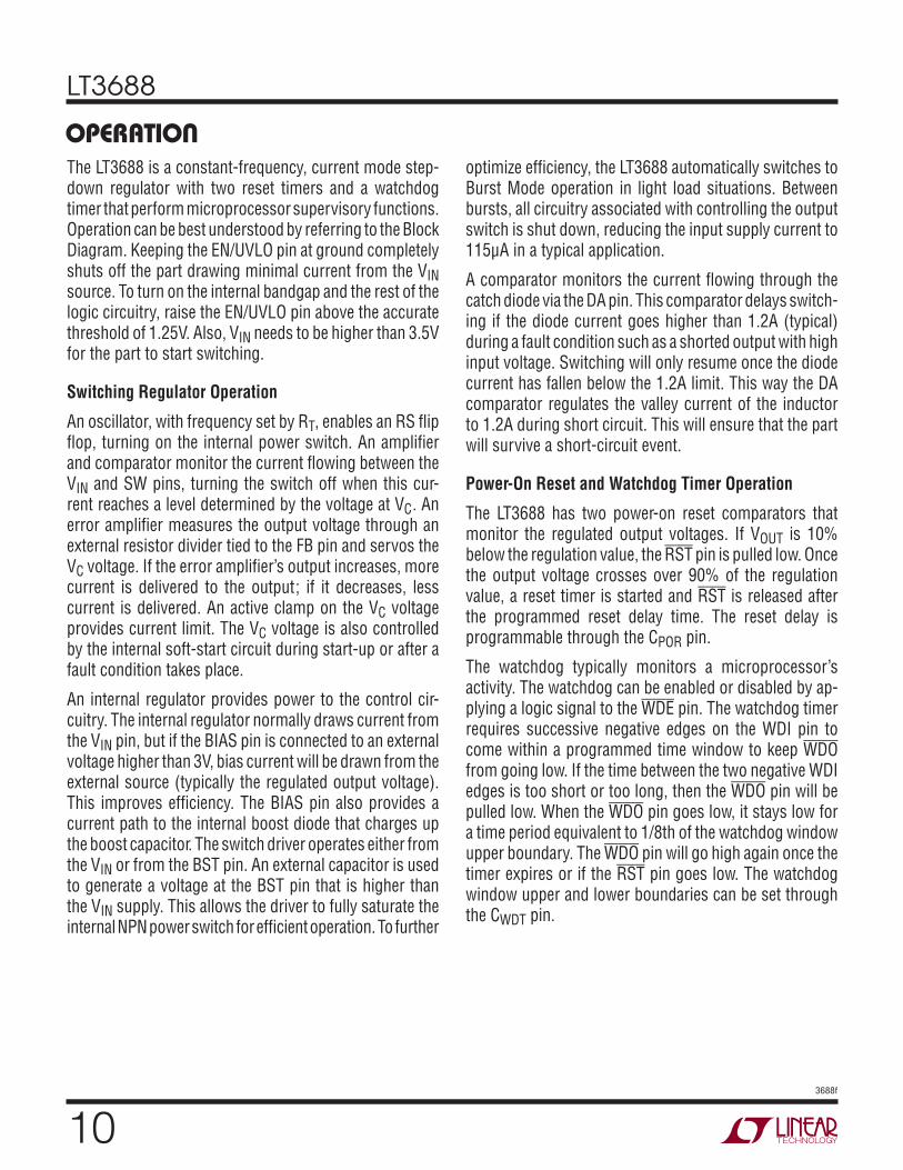
Power-On Reset and Watchdog Timer Operation
The LT3688 has two power-on reset comparators that monitor the regulated output voltages. If VOUT is 10% below the regulation value, the RST pin is pulled low. Once the output voltage crosses over 90% of the regulation value, a reset timer is started and RST is released after the programmed reset delay time. The reset delay is programmable through the CPOR pin.
The watchdog typically monitors a microprocessor’s activity. The watchdog can be enabled or disabled by ap-plying a logic signal to the WDE pin. The watchdog timer requires successive negative edges on the WDI pin to come within a programmed time window to keep WDO from going low. If the time between the two negative WDI edges is too short or too long, then the WDO pin will be pulled low. When the WDO pin goes low, it stays low for a time period equivalent to 1/8th of the watchdog window upper boundary. The WDO pin will go high again once the timer expires or if the RST pin goes low. The watchdog window upper and lower boundaries can be set through the CWDT pin.
LT3688
113688f
TIMING DIAGRAMS
3686 TD01
tWDU
t < tWDL tWDTO
tWDTO
WDI
WDO
tRSTtUV
VOUTVUV
RST
Power-On Reset Timing
Watchdog Timing
LT3688
123688f
TIMING DIAGRAMS
tWDU
tRST2
tRST1
VOUT1
VOUT2
VUV
VUV
RST1
RST2
WDO
STARTUP TIMING (VCONFIG = HIGH)
WDI
tWDU
tRST2
tRST1
VOUT1
VOUT2
VUV
VUV
RST1
RST2
WDO
STARTUP TIMING (VCONFIG = OPEN)
WDI
tWDU
tRST1
VOUT1
RST1
VUV
VUV
VOUT2
RST2
WDO
STARTUP TIMING (VCONFIG = LOW)
WDI
tRST1 = PROGRAMMED RESET PERIOD (CPOR1)tRST2 = PROGRAMMED RESET PERIOD (CPOR2)tWDU = WATCHDOG WINDOW UPPER BOUNDRYVUV = RESET THRESHOLD
3688 TD
LT3688
133688f
APPLICATIONS INFORMATIONSetting the Output Voltage
The output voltage is programmed with a resistor divider between the output and the FB pin. Choose the 1% resistors according to:
R1= R2
VOUT
0.8V– 1
⎛⎝⎜
⎞⎠⎟
For reference designators, refer to the Block Diagram.
Setting the Switching Frequency
The LT3688 uses a constant-frequency PWM architecture that can be programmed to switch from 350 kHz to 2.2 MHz by using a resistor tied from the RT pin to ground. Table 1 shows the RT values for various switching frequencies
Table 1. Switching Frequency vs RT
SWITCHING FREQUENCY (MHz)RT
(kΩ)
0.35 165
0.5 110
0.6 88.7
0.7 75
0.8 64.9
0.9 56.2
1 49.9
1.2 40.2
1.4 33.2
1.6 27.4
1.8 23.2
2.1 20
2.3 17.4
Operating Frequency Tradeoffs
Selection of the operating frequency is a tradeoff between effi ciency, component size and maximum input voltage. The advantage of high frequency operation is that smaller inductor and capacitor values may be used. The disadvantages are lower effi ciency, and narrower input voltage range at constant-frequency. The highest constant-switching frequency (fSW(MAX)) for a given application can be calculated as follows:
fSW(MAX) = VOUT + VF
tON(MIN) VIN + VF – VSW( )
where VIN is the typical input voltage, VOUT is the output voltage, VF is the catch diode drop (~0.5V) and VSW is the internal switch drop (~0.3V at maximum load). If the LT3688 is programmed to operate at a frequency higher than fSW(MAX) for a given input voltage, the LT3688 enters pulse skip mode, where it skips switching cycles to maintain regulation. At frequencies higher than fSW(MAX), the LT3688 no longer operates with constant frequency. The LT3688 enters pulse skip mode at frequencies higher than fSW(MAX) because of the limitation on the LT3688’s minimum on time of 140ns (180ns for TJ > 125°C). As the switching frequency is increased above fSW(MAX), the part is required to switch for shorter periods to maintain the same duty cycle. Delays associated with turning off the power switch dictate the minimum on-time of the part. When the required on-time decreases below the minimum on-time of 140ns, the switch pulse width remains fi xed at 140ns (instead of becoming narrower) to accommodate the same duty cycle require-ment. The inductor current ramps up to a value exceeding the load current and the output ripple increases. The part then remains off until the output voltage dips below the programmed value before it begins switching again.
Maximum Operating Voltage Range
The maximum input voltage for LT3688 applications depends on switching frequency, the absolute maximum ratings of the VIN and BST pins, and by the minimum duty cycle (DCMIN). The LT3688 can operate from input voltages up to 36V.
DCMIN = tON(MIN) • fSW
where tON(MIN) is equal to 140ns and fSW is the switching frequency. Running at a lower switching frequency allows a lower minimum duty cycle. The maximum input voltage before pulse-skipping occurs depends on the output volt-age and the minimum duty cycle:
VIN(PS) = VOUT + VF
DCMIN
– VF + VSW
Example: f = 2.1MHz, VOUT = 3.3V
DCMIN = 140ns • 2.1MHz = 0.294
VIN(PS) = 3.3V + 0.5V
0.294– 0.5V + 0.3V = 12.7V
LT3688
143688f
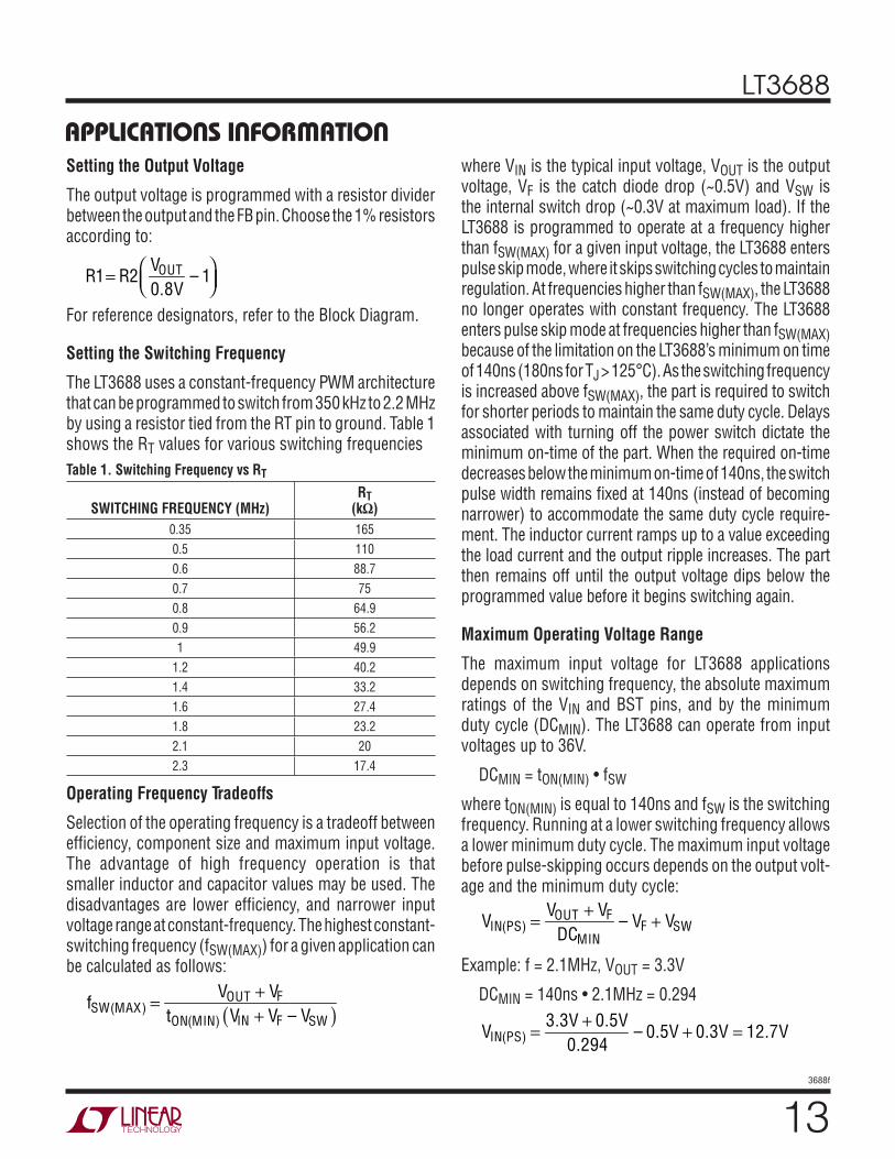
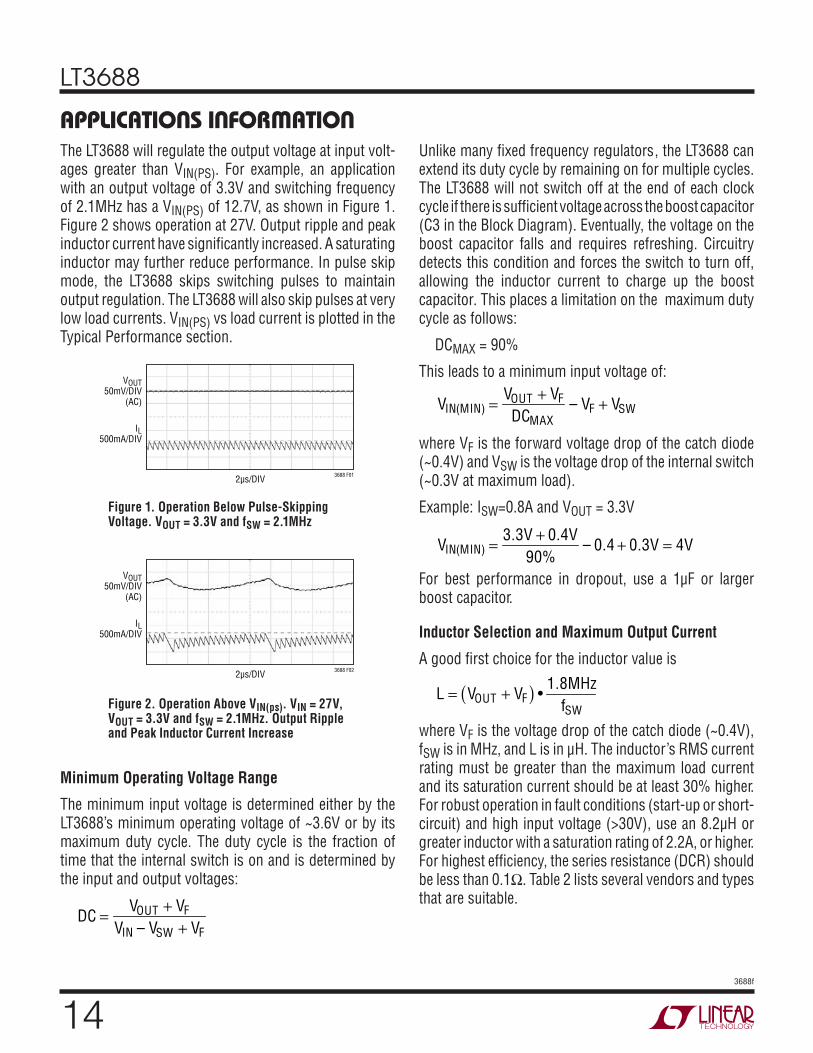
APPLICATIONS INFORMATIONThe LT3688 will regulate the output voltage at input volt-ages greater than VIN(PS). For example, an application with an output voltage of 3.3V and switching frequency of 2.1MHz has a VIN(PS) of 12.7V, as shown in Figure 1. Figure 2 shows operation at 27V. Output ripple and peak inductor current have signifi cantly increased. A saturating inductor may further reduce performance. In pulse skip mode, the LT3688 skips switching pulses to maintain output regulation. The LT3688 will also skip pulses at very low load currents. VIN(PS) vs load current is plotted in the Typical Performance section.
VOUT50mV/DIV
(AC)
IL500mA/DIV
2μs/DIV3688 F01
Figure 1. Operation Below Pulse-Skipping Voltage. VOUT = 3.3V and fSW = 2.1MHz
VOUT50mV/DIV
(AC)
IL500mA/DIV
2μs/DIV3688 F02
Figure 2. Operation Above VIN(ps). VIN = 27V, VOUT = 3.3V and fSW = 2.1MHz. Output Ripple and Peak Inductor Current Increase
Minimum Operating Voltage Range
The minimum input voltage is determined either by the LT3688’s minimum operating voltage of ~3.6V or by its maximum duty cycle. The duty cycle is the fraction of time that the internal switch is on and is determined by the input and output voltages:
DC = VOUT + VF
VIN – VSW + VF
Unlike many fi xed frequency regulators, the LT3688 can extend its duty cycle by remaining on for multiple cycles. The LT3688 will not switch off at the end of each clock cycle if there is suffi cient voltage across the boost capacitor (C3 in the Block Diagram). Eventually, the voltage on the boost capacitor falls and requires refreshing. Circuitry detects this condition and forces the switch to turn off, allowing the inductor current to charge up the boost capacitor. This places a limitation on the maximum duty cycle as follows:
DCMAX = 90%
This leads to a minimum input voltage of:
VIN(MIN) = VOUT + VF
DCMAX
– VF + VSW
where VF is the forward voltage drop of the catch diode (~0.4V) and VSW is the voltage drop of the internal switch (~0.3V at maximum load).
Example: ISW=0.8A and VOUT = 3.3V
VIN(MIN) = 3.3V + 0.4V
90%– 0.4 + 0.3V = 4V
For best performance in dropout, use a 1μF or larger boost capacitor.
Inductor Selection and Maximum Output Current
A good fi rst choice for the inductor value is
L = VOUT + VF( ) •
1.8MHz
fSW
where VF is the voltage drop of the catch diode (~0.4V), fSW is in MHz, and L is in μH. The inductor’s RMS current rating must be greater than the maximum load current and its saturation current should be at least 30% higher. For robust operation in fault conditions (start-up or short-circuit) and high input voltage (>30V), use an 8.2μH or greater inductor with a saturation rating of 2.2A, or higher. For highest effi ciency, the series resistance (DCR) should be less than 0.1Ω. Table 2 lists several vendors and types that are suitable.
LT3688
153688f
APPLICATIONS INFORMATIONTable 2. Inductor Vendors
VENDOR PART SERIES TYPE URL
Murata LQH55D Open www.murata.com
TDK SLF7045SLF10145
ShieldedShielded
www.component.tdk.com
Toko DC62CBD63CBD75CD75F
ShieldedShieldedShielded
Open
www.toko.com
Sumida CR54CDRH74
CDRH6D38CR75
OpenShieldedShielded
Open
www.sumida.com
The optimum inductor for a given application may differ from the one indicated by this simple design guide. A larger value inductor provides a higher maximum load current, and reduces the output voltage ripple. If your load is lower than the maximum load current, then you can relax the value of the inductor and operate with higher ripple current. This allows you to use a physically smaller inductor, or one with a lower DCR resulting in higher effi ciency. Be aware that if the inductance differs from the simple rule above, then the maximum load current will depend on input voltage. In addition, low inductance may result in discontinuous mode operation, which further reduces maximum load current. Discontinuous operation occurs when IOUT is less than ΔIL / 2. For details of maximum output current and discontinuous mode operation, see Linear Technology’s Application Note AN44. Finally, for duty cycles greater than 50% (VOUT/VIN > 0.5), a minimum inductance is required to avoid sub-harmonic oscillations:
LMIN = VOUT + VF( ) •
1.2MHz
fSW
where VF is the voltage drop of the catch diode (~0.4V), fSW is in MHz, and LMIN is in μH.
The current in the inductor is a triangle wave with an average value equal to the load current. The peak switch current is equal to the output current plus half the peak-to-peak inductor ripple current. The LT3688 limits its switch cur-rent in order to protect itself and the system from overload faults. Therefore, the maximum output current that the LT3688 will deliver depends on the switch current limit, the inductor value, and the input and output voltages.
When the switch is off, the potential across the induc-tor is the output voltage plus the catch diode drop. This gives the peak-to-peak ripple current in the inductor
ΔIL =
1– DC( ) VOUT + VF( )L • f
where f is the switching frequency of the LT3688 and L is the value of the inductor. The peak inductor and switch current is
ISW(PK) = IL(PK) = IOUT + ΔIL
2
To maintain output regulation, this peak current must be less than the LT3688’s switch current limit ILIM. ILIM is at least 1.25A for at low duty cycles and decreases linearly to 0.9A at DC = 0.9. The maximum output current is a function of the chosen inductor value:
IOUT(MAX) = ILIM –ΔIL2
= 1.25A • 1– 0.3DC( ) –ΔIL2
Choosing an inductor value so that the ripple current is small will allow a maximum output current near the switch current limit.
One approach to choosing the inductor is to start with the simple rule given above, look at the available inductors, and choose one to meet cost or space goals. Then use these equations to check that the LT3688 will be able to deliver the required output current. Note again that these equations assume that the inductor current is continuous.
Input Capacitor
Bypass the input of the LT3688 circuit with a ceramic capacitor of an X7R or X5R type. Y5V types have poor performance over temperature and applied voltage, and should not be used. A 2.2μF to 4.7μF ceramic capacitor is adequate to bypass the LT3688 and will easily handle the ripple current. Note that larger input capacitance is required when a lower switching frequency is used. If the input power source has high impedance, or there is signifi cant inductance due to long wires or cables,
LT3688
163688f
APPLICATIONS INFORMATIONadditional bulk capacitance may be necessary. This can be provided with a lower performance electrolytic capacitor. Step-down regulators draw current from the input supply in pulses with very fast rise and fall times. The input capacitor is required to reduce the resulting voltage ripple at the LT3688 input and to force this very high frequency switching current into a tight local loop, minimizing EMI. A 2.2μF capacitor is capable of this task, but only if it is placed close to the LT3688 and the catch diode (see the PCB Layout section). A second precaution regarding the ceramic input capacitor concerns the maximum input voltage rating of the LT3688. A ceramic input capacitor combined with trace or cable inductance forms a high quality (under damped) tank circuit. If the LT3688 circuit is plugged into a live supply, the input voltage can ring to twice its nominal value, possibly exceeding the LT3688’s voltage rating. See Linear Technology’s Application Note 88 for details.
Output Capacitor and Output Ripple
The output capacitor has two essential functions. Along with the inductor, it fi lters the square wave generated by the LT3688 to produce the DC output. In this role it determines the output ripple, and low impedance at the switching frequency is important. The second function is to store energy in order to satisfy transient loads and stabilize the LT3688’s control loop. Ceramic capacitors have very low equivalent series resistance (ESR) and provide the best ripple performance. A good starting value is:
COUT = 50
VOUT • fSW
where fSW is in MHz and COUT is the recommended output capacitance in μF. Use X5R or X7R types, which will provide low output ripple and good transient response. Transient performance can be improved with a high value capacitor, but a phase lead capacitor across the feedback resistor R1 may be required to get the full benefi t (see the Compensation section).
High performance electrolytic capacitors can be used for the output capacitor. Low ESR is important, so choose one that is intended for use in switching regulators. The ESR should be specifi ed by the supplier and should be 0.1Ω or less. Such a capacitor will be larger than a ceramic capacitor and will have a larger capacitance because the capacitor must be large to achieve low ESR. Table 3 lists several capacitor vendors.
Table 3. Capacitor Vendors
VENDOR PART SERIES COMMENTS
Panasonic CeramicPolymerTantalum
EEEF Series
Kemet CeramicTantalum T494, T495
Sanyo CeramicPolymerTantalum
POSCAP
Murata Ceramic
AVX CeramicTantalum TPS Series
Taiyo Yuden Ceramic
Catch Diode
The catch diode conducts current only during switch-off time. Average forward current in normal operation can be calculated from:
ID(AVG) =
IOUT VIN – VOUT( )VIN
where IOUT is the output load current. The only reason to consider a diode with a larger current rating than neces-sary for nominal operation is for the worst-case condition of shorted output. The diode current will then increase to the typical peak switch current limit. Peak reverse voltage is equal to the regulator input voltage. Use a Schottky diode with a reverse voltage rating greater than the input voltage. Table 4 lists several Schottky diodes and their manufacturers.
LT3688
173688f
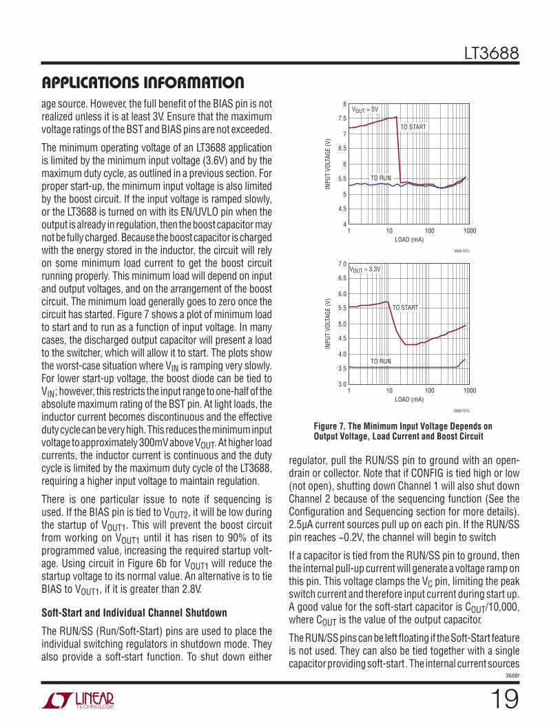
Table 4. Capacitor Vendors
Part NumberVR(V)
IAVE (A)
VF at 1A(mV)
On Semiconductor
MBR0520L 20 0.5
MBR0540 40 0.5 620
MBRM120E 20 1 530
MBRM140 40 1 550
Diodes Inc.
B0530W 30 0.5
B120 20 1 500
B130 30 1 500
B140HB 40 1
DFLS140 40 1.1 510
Ceramic Capacitors
Ceramic capacitors are small, robust and have very low ESR. However, ceramic capacitors can cause problems when used with the LT3688 due to their piezoelectric nature. When in Burst Mode operation, the LT3688’s switching frequency depends on the load current, and at very light loads the LT3688 can excite the ceramic capacitor at audio frequencies, generating audible noise. Since the LT3688 operates at a lower current limit during Burst Mode operation, the noise is typically very quiet. If this is unacceptable, use a high performance tantalum or electrolytic capacitor at the output.
Frequency Compensation
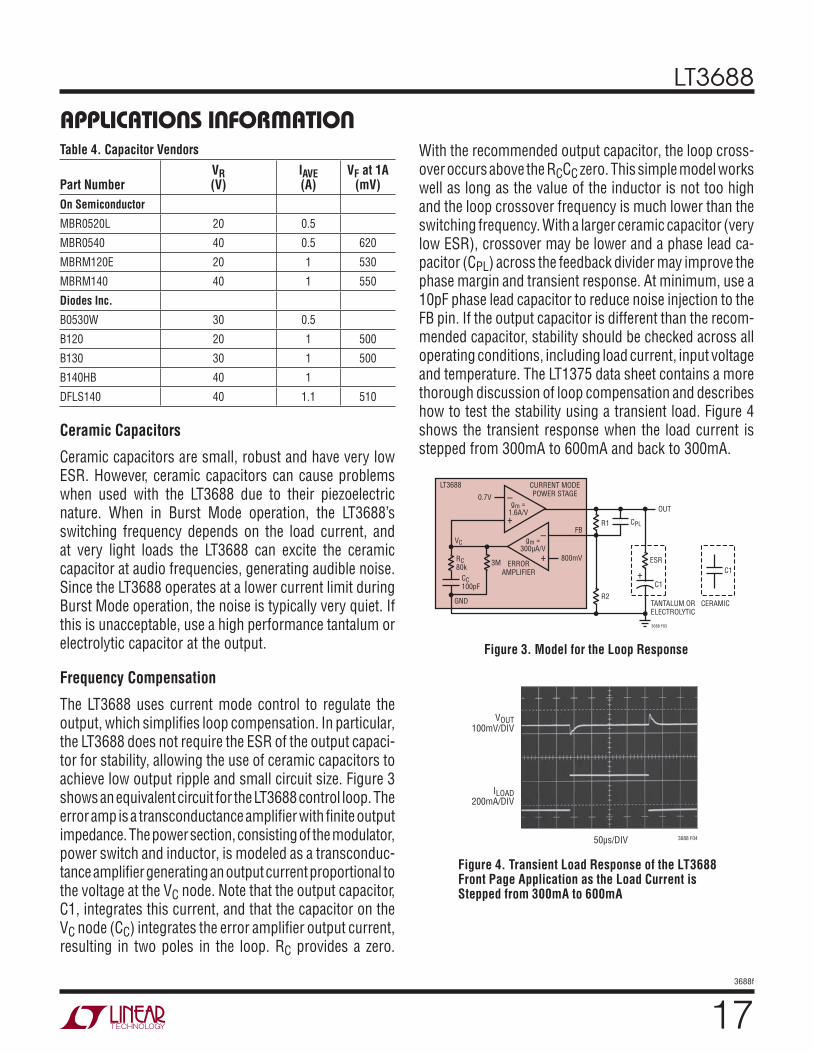
The LT3688 uses current mode control to regulate the output, which simplifi es loop compensation. In particular, the LT3688 does not require the ESR of the output capaci-tor for stability, allowing the use of ceramic capacitors to achieve low output ripple and small circuit size. Figure 3 shows an equivalent circuit for the LT3688 control loop. The error amp is a transconductance amplifi er with fi nite output impedance. The power section, consisting of the modulator, power switch and inductor, is modeled as a transconduc-tance amplifi er generating an output current proportional to the voltage at the VC node. Note that the output capacitor, C1, integrates this current, and that the capacitor on the VC node (CC) integrates the error amplifi er output current, resulting in two poles in the loop. RC provides a zero.
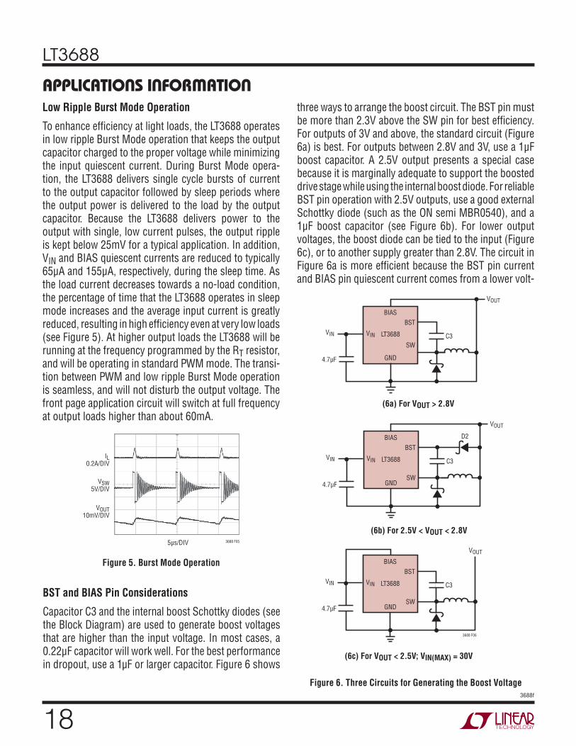
With the recommended output capacitor, the loop cross-over occurs above the RCCC zero. This simple model works well as long as the value of the inductor is not too high and the loop crossover frequency is much lower than the switching frequency. With a larger ceramic capacitor (very low ESR), crossover may be lower and a phase lead ca-pacitor (CPL) across the feedback divider may improve the phase margin and transient response. At minimum, use a 10pF phase lead capacitor to reduce noise injection to the FB pin. If the output capacitor is different than the recom-mended capacitor, stability should be checked across all operating conditions, including load current, input voltage and temperature. The LT1375 data sheet contains a more thorough discussion of loop compensation and describes how to test the stability using a transient load. Figure 4 shows the transient response when the load current is stepped from 300mA to 600mA and back to 300mA.
–
+
800mV
VC
LT3688
GND
3688 F03
R1
OUT
ESR
TANTALUM OR ELECTROLYTIC
CERAMIC
ERRORAMPLIFIER
CURRENT MODEPOWER STAGE
FB
R2
3MRC80k
CC100pF C1
C1
gm =1.6A/V
+
CPL
0.7V
–
+
gm =300μA/V
Figure 3. Model for the Loop Response
Figure 4. Transient Load Response of the LT3688 Front Page Application as the Load Current is Stepped from 300mA to 600mA
APPLICATIONS INFORMATION
VOUT100mV/DIV
ILOAD200mA/DIV
50μs/DIV 3688 F04
LT3688
183688f
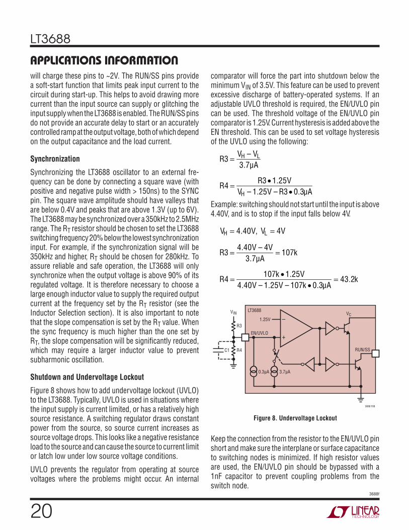
Low Ripple Burst Mode Operation
To enhance effi ciency at light loads, the LT3688 operates in low ripple Burst Mode operation that keeps the output capacitor charged to the proper voltage while minimizing the input quiescent current. During Burst Mode opera-tion, the LT3688 delivers single cycle bursts of current to the output capacitor followed by sleep periods where the output power is delivered to the load by the output capacitor. Because the LT3688 delivers power to the output with single, low current pulses, the output ripple is kept below 25mV for a typical application. In addition, VIN and BIAS quiescent currents are reduced to typically 65μA and 155μA, respectively, during the sleep time. As the load current decreases towards a no-load condition, the percentage of time that the LT3688 operates in sleep mode increases and the average input current is greatly reduced, resulting in high effi ciency even at very low loads (see Figure 5). At higher output loads the LT3688 will be running at the frequency programmed by the RT resistor, and will be operating in standard PWM mode. The transi-tion between PWM and low ripple Burst Mode operation is seamless, and will not disturb the output voltage. The front page application circuit will switch at full frequency at output loads higher than about 60mA.
IL0.2A/DIV
VSW5V/DIV
VOUT10mV/DIV
5μs/DIV 3688 F05
Figure 5. Burst Mode Operation
BST and BIAS Pin Considerations
Capacitor C3 and the internal boost Schottky diodes (see the Block Diagram) are used to generate boost voltages that are higher than the input voltage. In most cases, a 0.22μF capacitor will work well. For the best performance in dropout, use a 1μF or larger capacitor. Figure 6 shows
VIN
BST
SW
BIAS
VIN
VOUT
4.7μF
C3
GND
LT3688
(6a) For VOUT > 2.8V
Figure 6. Three Circuits for Generating the Boost Voltage
VIN
BST
SW
BIAS
VIN
VOUT
4.7μF
C3
D2
GND
LT3688
(6b) For 2.5V < VOUT < 2.8V
VIN
BST
SW
BIAS
VIN
VOUT
4.7μF
C3
GND
LT3688
3688 F06
(6c) For VOUT < 2.5V; VIN(MAX) = 30V
APPLICATIONS INFORMATIONthree ways to arrange the boost circuit. The BST pin must be more than 2.3V above the SW pin for best effi ciency. For outputs of 3V and above, the standard circuit (Figure 6a) is best. For outputs between 2.8V and 3V, use a 1μF boost capacitor. A 2.5V output presents a special case because it is marginally adequate to support the boosted drive stage while using the internal boost diode. For reliable BST pin operation with 2.5V outputs, use a good external Schottky diode (such as the ON semi MBR0540), and a 1μF boost capacitor (see Figure 6b). For lower output voltages, the boost diode can be tied to the input (Figure 6c), or to another supply greater than 2.8V. The circuit in Figure 6a is more effi cient because the BST pin current and BIAS pin quiescent current comes from a lower volt-
LT3688
193688f
age source. However, the full benefi t of the BIAS pin is not realized unless it is at least 3V. Ensure that the maximum voltage ratings of the BST and BIAS pins are not exceeded.
The minimum operating voltage of an LT3688 application is limited by the minimum input voltage (3.6V) and by the maximum duty cycle, as outlined in a previous section. For proper start-up, the minimum input voltage is also limited by the boost circuit. If the input voltage is ramped slowly, or the LT3688 is turned on with its EN/UVLO pin when the output is already in regulation, then the boost capacitor may not be fully charged. Because the boost capacitor is charged with the energy stored in the inductor, the circuit will rely on some minimum load current to get the boost circuit running properly. This minimum load will depend on input and output voltages, and on the arrangement of the boost circuit. The minimum load generally goes to zero once the circuit has started. Figure 7 shows a plot of minimum load to start and to run as a function of input voltage. In many cases, the discharged output capacitor will present a load to the switcher, which will allow it to start. The plots show the worst-case situation where VIN is ramping very slowly. For lower start-up voltage, the boost diode can be tied to VIN; however, this restricts the input range to one-half of the absolute maximum rating of the BST pin. At light loads, the inductor current becomes discontinuous and the effective duty cycle can be very high. This reduces the minimum input voltage to approximately 300mV above VOUT. At higher load currents, the inductor current is continuous and the duty cycle is limited by the maximum duty cycle of the LT3688, requiring a higher input voltage to maintain regulation.
There is one particular issue to note if sequencing is used. If the BIAS pin is tied to VOUT2, it will be low during the startup of VOUT1. This will prevent the boost circuit from working on VOUT1 until it has risen to 90% of its programmed value, increasing the required startup volt-age. Using circuit in Figure 6b for VOUT1 will reduce the startup voltage to its normal value. An alternative is to tie BIAS to VOUT1, if it is greater than 2.8V.
Soft-Start and Individual Channel Shutdown
The RUN/SS (Run/Soft-Start) pins are used to place the individual switching regulators in shutdown mode. They also provide a soft-start function. To shut down either
Figure 7. The Minimum Input Voltage Depends on Output Voltage, Load Current and Boost Circuit
regulator, pull the RUN/SS pin to ground with an open-drain or collector. Note that if CONFIG is tied high or low (not open), shutting down Channel 1 will also shut down Channel 2 because of the sequencing function (See the Confi guration and Sequencing section for more details). 2.5μA current sources pull up on each pin. If the RUN/SS pin reaches ~0.2V, the channel will begin to switch
If a capacitor is tied from the RUN/SS pin to ground, then the internal pull-up current will generate a voltage ramp on this pin. This voltage clamps the VC pin, limiting the peak switch current and therefore input current during start up. A good value for the soft-start capacitor is COUT/10,000, where COUT is the value of the output capacitor.
The RUN/SS pins can be left fl oating if the Soft-Start feature is not used. They can also be tied together with a single capacitor providing soft-start. The internal current sources
APPLICATIONS INFORMATION
LOAD (mA)
TO START
VOUT = 5V
TO RUN
1 10 100 10004
INP
UT V
OLT
AG
E (
V)
7
7.5
6
6.5
4.5
5
5.5
8
3688 F07a
LOAD (mA)
1 10 100 10003.0
INP
UT V
OLT
AG
E (
V)
6.0
6.5
5.0
5.5
3.5
4.0
4.5
7.0
3688 F07b
TO START
TO RUN
VOUT = 3.3V
LT3688
203688f
will charge these pins to ~2V. The RUN/SS pins provide a soft-start function that limits peak input current to the circuit during start-up. This helps to avoid drawing more current than the input source can supply or glitching the input supply when the LT3688 is enabled. The RUN/SS pins do not provide an accurate delay to start or an accurately controlled ramp at the output voltage, both of which depend on the output capacitance and the load current.
Synchronization
Synchronizing the LT3688 oscillator to an external fre-quency can be done by connecting a square wave (with positive and negative pulse width > 150ns) to the SYNC pin. The square wave amplitude should have valleys that are below 0.4V and peaks that are above 1.3V (up to 6V). The LT3688 may be synchronized over a 350kHz to 2.5MHz range. The RT resistor should be chosen to set the LT3688 switching frequency 20% below the lowest synchronization input. For example, if the synchronization signal will be 350kHz and higher, RT should be chosen for 280kHz. To assure reliable and safe operation, the LT3688 will only synchronize when the output voltage is above 90% of its regulated voltage. It is therefore necessary to choose a large enough inductor value to supply the required output current at the frequency set by the RT resistor (see the Inductor Selection section). It is also important to note that the slope compensation is set by the RT value. When the sync frequency is much higher than the one set by RT, the slope compensation will be signifi cantly reduced, which may require a larger inductor value to prevent subharmonic oscillation.
Shutdown and Undervoltage Lockout
Figure 8 shows how to add undervoltage lockout (UVLO) to the LT3688. Typically, UVLO is used in situations where the input supply is current limited, or has a relatively high source resistance. A switching regulator draws constant power from the source, so source current increases as source voltage drops. This looks like a negative resistance load to the source and can cause the source to current limit or latch low under low source voltage conditions.
UVLO prevents the regulator from operating at source voltages where the problems might occur. An internal
comparator will force the part into shutdown below the minimum VIN of 3.5V. This feature can be used to prevent excessive discharge of battery-operated systems. If an adjustable UVLO threshold is required, the EN/UVLO pin can be used. The threshold voltage of the EN/UVLO pin comparator is 1.25V. Current hysteresis is added above the EN threshold. This can be used to set voltage hysteresis of the UVLO using the following:
R3 = VH – VL
3.7μA
R4 = R3• 1.25V
VH – 1.25V – R3 • 0.3μA
Example: switching should not start until the input is above 4.40V, and is to stop if the input falls below 4V.
VH = 4.40V, VL = 4V
R3 = 4.40V – 4V
3.7μA= 107k
R4 = 107k • 1.25V
4.40V – 1.25V – 107k • 0.3μA= 43.2k
1.25V
3.7μA0.3μA
R3
R4C1
EN/UVLO
LT3688VIN
RUN/SS
VC
3688 F08
–
+
Figure 8. Undervoltage Lockout
APPLICATIONS INFORMATION
Keep the connection from the resistor to the EN/UVLO pin short and make sure the interplane or surface capacitance to switching nodes is minimized. If high resistor values are used, the EN/UVLO pin should be bypassed with a 1nF capacitor to prevent coupling problems from the switch node.
LT3688
213688f
Output Voltage Monitoring
The LT3688 provides power supply monitoring for microprocessor-based systems. The features include power-on reset (POR) and watchdog timing.
A precise internal voltage reference and glitch immune precision POR comparator circuits monitor the LT3688 output voltages. Each channel’s output voltage must be above 90% of the programmed value for RST not to be asserted (refer to the Timing Diagram). The LT3688 will assert RST during power-up, power-down and brownout conditions. Once the output voltage rises above the RST threshold, the adjustable reset timer is started and RST is released after the reset timeout period. On power-down, once the output voltage drops below RST threshold, RST is held at a logic low. The reset timer is adjustable using external capacitors. This capability helps hold the micro-processor in a stable shutdown condition. The RST pin has weak pull-up to the BIAS pin.
The above discussion is concerned only with the DC value of the monitored supply. Real supplies also have relatively high-frequency variation, from sources such as load transients, noise, and pickup. These variations should not be considered by the monitor in determining whether a supply voltage is valid or not. The variations may cause spurious outputs at RST, particularly if the supply voltage is near its trip threshold.
Two techniques are used to combat spurious reset without sacrifi cing threshold accuracy. First, the timeout period helps prevent high-frequency variation whose frequency is above 1/ tRST from appearing at the RST output. When the voltage at FB goes below the threshold, the RST pin asserts low. When the supply recovers past the threshold, the reset timer starts (assuming it is not disabled), and RST does not go high until it fi nishes. If the supply becomes invalid any time during the timeout period, the timer resets and starts fresh when the supply next becomes valid. While the reset timeout is useful for preventing toggling of the reset output in most cases, it is not effective at preventing nuisance resets due to short glitches (due to load transients or other effects) on a valid supply. To reduce sensitivity to these short glitches, the comparator has additional anti-glitch
circuitry. Any transient at the input of the comparator needs to be of suffi cient magnitude and duration (tUV) before it can change the monitor state. The combination of the reset timeout and anti-glitch circuitry prevents spurious changes in output state without sacrifi cing threshold accuracy.
Watchdog Timer
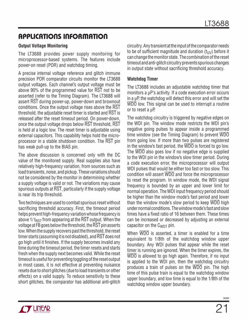
The LT3688 includes an adjustable watchdog timer that monitors a μP’s activity. If a code execution error occurs in a μP, the watchdog will detect this error and will set the WDO low. This signal can be used to interrupt a routine or to reset a μP.
The watchdog circuitry is triggered by negative edges on the WDI pin. The window mode restricts the WDI pin’s negative going pulses to appear inside a programmed time window (see the Timing Diagram) to prevent WDO from going low. If more than two pulses are registered in the window’s fast period, the WDO is forced to go low. The WDO also goes low if no negative edge is supplied to the WDI pin in the window’s slow timer period. During a code execution error, the microprocessor will output WDI pulses that would be either too fast or too slow. This condition will assert WDO and force the microprocessor to reset the program. In window mode, the WDI signal frequency is bounded by an upper and lower limit for normal operation. The WDI input frequency period should be higher than the window mode’s fast period and lower than the window mode’s slow period to keep WDO high under normal conditions. The window mode’s fast and slow times have a fi xed ratio of 16 between them. These times can be increased or decreased by adjusting an external capacitor on the CWDT pin.
When WDO is asserted, a timer is enabled for a time equivalent to 1/8th of the watchdog window upper boundary. Any WDI pulses that appear while the reset timer is running are ignored. When the timer expires, the WDO is allowed to go high again. Therefore, if no input is applied to the WDI pin, then the watchdog circuitry produces a train of pulses on the WDO pin. The high time of this pulse train is equal to the watchdog window upper boundary, and low time is equal to the 1/8th of the watchdog window upper boundary.
APPLICATIONS INFORMATION
LT3688
223688f
If WDO is low and RST goes low, then WDO will go high. The WDE pin allows the user to turn on and off the watchdog function. Leaving this pin open is okay and will automatically enable the watchdog. It has an internal weak pull-down to ground. The WDI pin has an internal weak pull-up that keeps the WDI pin high. If watchdog is disabled, leaving this pin open is acceptable.
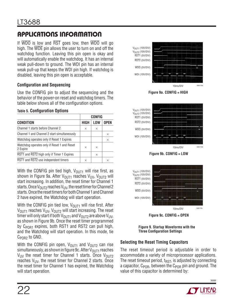
Confi guration and Sequencing
Use the CONFIG pin to adjust the sequencing and the behavior of the power-on reset and watchdog timers. The table below shows all of the confi guration options.
Table 5. Confi guration Options
CONFIG
CONDITION HIGH LOW OPEN
Channel 1 starts before Channel 2 × ×Channel 1 and Channel 2 start simultaneously ×Watchdog operates only if Reset 1 Expires ×Watchdog operates only if Reset 1 and Reset 2 Expire
× ×
RST1 and RST2 high only if Timer 1 Expires ×RST1 and RST2 use independent timers × ×
Figure 9b. CONFIG = LOW
APPLICATIONS INFORMATION
Figure 9. Startup Waveforms with the Three Confi guration Settings
With the CONFIG pin tied high, VOUT1 will rise fi rst, as shown in Figure 9a. After VOUT1 reaches VUV, VOUT2 will start increasing. In addition, the reset timer for Channel 1 starts. Once VOUT2 reaches VUV, the reset timer for Channel 2 starts. Once the reset timers for both Channel 1 and Channel 2 have expired, the Watchdog will start operation.
With the CONFIG pin tied low, VOUT1 will rise fi rst. After VOUT1 reaches VUV, VOUT2 will start increasing. The reset timer will only start if both VOUT1 and VOUT2 are above VUV, as shown in Figure 9b. Once the reset timer programmed by CPOR1 expires, both RST1 and RST2 can pull high, and the Watchdog will start operation. In this mode, tie CPOR2 to GND.
With the CONFIG pin open, VOUT1 and VOUT2 can rise simultaneously, as shown in fi gure 9c. After VOUT1 reaches VUV the reset timer for Channel 1 starts. Once VOUT2 reaches VUV, the reset timer for Channel 2 starts. Once the reset timer for Channel 1 has expired, the Watchdog will start operation.
Figure 9a. CONFIG = HIGH
Figure 9c. CONFIG = OPEN
VOUT1 (10V/DIV)
VOUT2 (10V/DIV)
RST1 (5V/DIV)
RST2 (5V/DIV)
WDO (5V/DIV)
WDI (10V/DIV)
10ms/DIV 3688 F09a
VOUT1 (10V/DIV)
VOUT2 (10V/DIV)
RST1 (5V/DIV)
RST2 (5V/DIV)
WDO (5V/DIV)
WDI (10V/DIV)
10ms/DIV 3688 F09b
VOUT1 (10V/DIV)
VOUT2 (10V/DIV)
RST1 (5V/DIV)
RST2 (5V/DIV)
WDO (5V/DIV)
WDI (10V/DIV)
10ms/DIV 3688 F09c
Selecting the Reset Timing Capacitors
The reset timeout period is adjustable in order to accommodate a variety of microprocessor applications. The reset timeout period, tRST, is adjusted by connecting a capacitor, CPOR, between the CPOR pin and ground. The value of this capacitor is determined by:
LT3688
233688f
CPOR = tRST • 200
pF
ms
⎛⎝⎜
⎞⎠⎟
This equation is accurate for reset timeout periods of 1ms, or greater. To program faster timeout periods, see the Reset Timeout Period vs Capacitance graph in the Typical Characteristics section. Leaving the CPOR pin unconnected will generate a minimum reset timeout of approximately 65μs. Maximum reset timeout is limited by the largest available low leakage capacitor. The accuracy of the timeout period will be affected by capacitor leakage (the nominal charging current is 2.5μA), capacitor tolerance and temperature coeffi cient. A low leakage, low tempco, capacitor is recommended.
Selecting the Watchdog Timing Capacitor
The watchdog timeout period is adjustable and can be optimized for software execution. The watchdog window upper boundary, tWDU is adjusted by connecting a capacitor, CWDT, between the CWDT pin and ground. Given a specifi ed watchdog timeout period, the capacitor is determined by:
CWDT = tWDU • 50
pF
ms
⎛⎝⎜
⎞⎠⎟
The window lower boundary (tWDL) and the watchdog timeout (tWDTO) have a fi xed relationship to tWDU for a given capacitor. The window lower boundary is related to tWDU by the following:
tWDL = 1
16• tWDU
The watchdog timeout is related to tWDU by the following:
tWDTO = 1
8•tWDU
Leaving the CWDT pin unconnected will generate a minimum watchdog window upper boundary of approximately 200μs. Maximum window upper boundary is limited by the largest available low leakage capacitor. The timing accuracy of the reset and watchdog signals depends on the initial accuracy and stability of the programing capacitors. Use capacitors with specifi ed accuracy, leakage and voltage and temperature coeffi cients. For surface mount ceramic capacitors C0G and NP0 types are superior to alternatives such as X5R and X7R.
APPLICATIONS INFORMATION
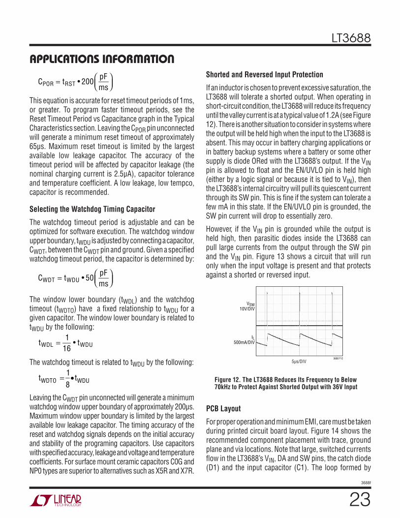
5μs/DIV
VSW10V/DIV
IL500mA/DIV
3688 F12
Figure 12. The LT3688 Reduces Its Frequency to Below 70kHz to Protect Against Shorted Output with 36V Input
Shorted and Reversed Input Protection
If an inductor is chosen to prevent excessive saturation, the LT3688 will tolerate a shorted output. When operating in short-circuit condition, the LT3688 will reduce its frequency until the valley current is at a typical value of 1.2A (see Figure 12). There is another situation to consider in systems where the output will be held high when the input to the LT3688 is absent. This may occur in battery charging applications or in battery backup systems where a battery or some other supply is diode ORed with the LT3688’s output. If the VIN pin is allowed to fl oat and the EN/UVLO pin is held high (either by a logic signal or because it is tied to VIN), then the LT3688’s internal circuitry will pull its quiescent current through its SW pin. This is fi ne if the system can tolerate a few mA in this state. If the EN/UVLO pin is grounded, the SW pin current will drop to essentially zero.
However, if the VIN pin is grounded while the output is held high, then parasitic diodes inside the LT3688 can pull large currents from the output through the SW pin and the VIN pin. Figure 13 shows a circuit that will run only when the input voltage is present and that protects against a shorted or reversed input.
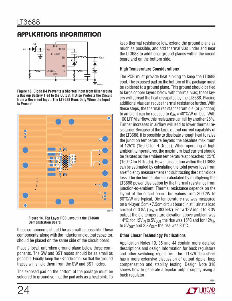
PCB Layout
For proper operation and minimum EMI, care must be taken during printed circuit board layout. Figure 14 shows the recommended component placement with trace, ground plane and via locations. Note that large, switched currents fl ow in the LT3688’s VIN, DA and SW pins, the catch diode (D1) and the input capacitor (C1). The loop formed by
LT3688
243688f
Figure 14. Top Layer PCB Layout in the LT3688 Demonstration Board
APPLICATIONS INFORMATION
3688 F14
these components should be as small as possible. These components, along with the inductor and output capacitor, should be placed on the same side of the circuit board.
Place a local, unbroken ground plane below these com-ponents. The SW and BST nodes should be as small as possible. Finally, keep the FB node small so that the ground traces will shield them from the SW and BST nodes.
The exposed pad on the bottom of the package must be soldered to ground so that the pad acts as a heat sink. To
keep thermal resistance low, extend the ground plane as much as possible, and add thermal vias under and near the LT3688 to additional ground planes within the circuit board and on the bottom side.
High Temperature Considerations
The PCB must provide heat sinking to keep the LT3688 cool. The exposed pad on the bottom of the package must be soldered to a ground plane. This ground should be tied to large copper layers below with thermal vias; these lay-ers will spread the heat dissipated by the LT3688. Placing additional vias can reduce thermal resistance further. With these steps, the thermal resistance from die (or junction) to ambient can be reduced to θJA = 40°C/W or less. With 100 LFPM airfl ow, this resistance can fall by another 25%. Further increases in airfl ow will lead to lower thermal re-sistance. Because of the large output current capability of the LT3688, it is possible to dissipate enough heat to raise the junction temperature beyond the absolute maximum of 125°C (150°C for H Grade). When operating at high ambient temperatures, the maximum load current should be derated as the ambient temperature approaches 125°C (150°C for H Grade). Power dissipation within the LT3688 can be estimated by calculating the total power loss from an effi ciency measurement and subtracting the catch diode loss. The die temperature is calculated by multiplying the LT3688 power dissipation by the thermal resistance from junction-to-ambient. Thermal resistance depends on the layout of the circuit board, but values from 30°C/W to 60°C/W are typical. Die temperature rise was measured on a 4-layer, 5cm • 7.5cm circuit board in still air at a load current of 0.8A (fSW = 800kHz). For a 12V input to 3.3V output the die temperature elevation above ambient was 14°C; for 12VIN to 5VOUT the rise was 15°C and for 12VIN to 5VOUT and 3.3VOUT the rise was 30°C.
Other Linear Technology Publications
Application Notes 19, 35 and 44 contain more detailed descriptions and design information for buck regulators and other switching regulators. The LT1376 data sheet has a more extensive discussion of output ripple, loop compensation and stability testing. Design Note 318 shows how to generate a bipolar output supply using a buck regulator.
VIN
3688 F13
EN/UVLO
BOOST
SW
LTC3688
BIAS
GND
DA
D4
FB
VIN
VOUT
+
Figure 13. Diode D4 Prevents a Shorted Input from Discharging a Backup Battery Tied to the Output; It Also Protects the Circuit from a Reversed Input. The LT3688 Runs Only When the Input Is Present
LT3688
253688f
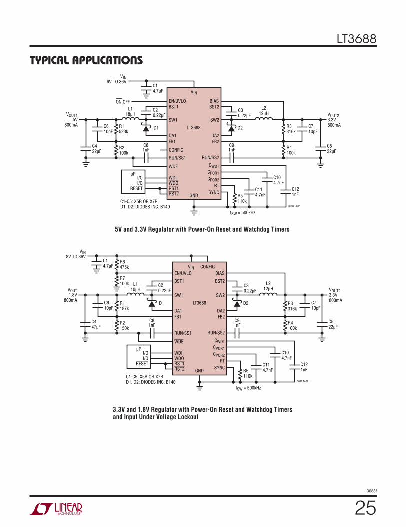
TYPICAL APPLICATIONS
CONFIG
VIN
LT3688
GND
BIASEN/UVLO
BST1C20.22μF
ON OFF
C14.7μF
VOUT15V
800mA
VIN6V TO 36V
C422μF
C610pF
C710pF
L118μH
L212μH
R1523k
R2100k
R3316k
R4100k
C81nF
C91nF
μP
C30.22μF
SW1
DA1
D2D1
BST2
SW2
DA2
FB1
RUN/SS1
WDE
WDIWDO
RST1
RST2
I/OI/O
RESET
FB2
RUN/SS2
CWDT
CPOR1
CPOR2
RT
SYNC
C522μF
C121nF
3688 TA02
C104.7nF
C114.7nFR5
110kC1-C5: X5R OR X7RD1, D2: DIODES INC. B140
fSW = 500kHz
VOUT23.3V800mA
5V and 3.3V Regulator with Power-On Reset and Watchdog Timers
CONFIGVIN
LT3688
GND
BIASEN/UVLO
BST1C20.22μFVOUT
1.8V800mA
VIN8V TO 36V
C447μF
C610pF
L110μH
L212μH
R1187k
R6475k
R7100k
R2150k
R3316k
R4100k
C81nF
C91nF
μP
C30.22μF
SW1
DA1
D2D1
BST2
SW2
DA2
FB1
RUN/SS1
WDE
WDIWDO
RST1
RST2
I/OI/O
RESET
FB2
RUN/SS2
CWDT
CPOR1
CPOR2
RT
SYNC
C522μF
C710pF
C121nF
3688 TA02
C104.7nF
C114.7nFR5
110kC1-C5: X5R OR X7RD1, D2: DIODES INC. B140
fSW = 500kHz
VOUT23.3V800mA
C14.7μF
3.3V and 1.8V Regulator with Power-On Reset and Watchdog Timers and Input Under Voltage Lockout
LT3688
263688f
TYPICAL APPLICATIONS
VIN
LT3688
GND
CONFIG
BIASEN/UVLO
BST1C20.1μF
ON OFF
C14.7μF
VOUT15V
800mA
VIN6V TO 36V
C410μF
C610μF
L18.2μH
L28.2μH
R1523k
R2100k
R3316k
R4100k
C81nF
C91nF
μP
C30.1μF
SW1
DA1
D2D1
BST2
SW2
DA2
FB1
RUN/SS1
WDE
WDIWDO
RST1
RST2
I/OI/O
RESET
FB2
RUN/SS2
CWDT
CPOR1
CPOR2
RT
SYNC
C522μF
C710pF
C121nF
3688 TA04
C104.7nF
C114.7nFR5
20kC1-C5: X5R OR X7RD1, D2: DIODES INC. B140
fSW = 2MHz: 8V < VIN < 16V, TJ < 85°C
VOUT23.3V800mA
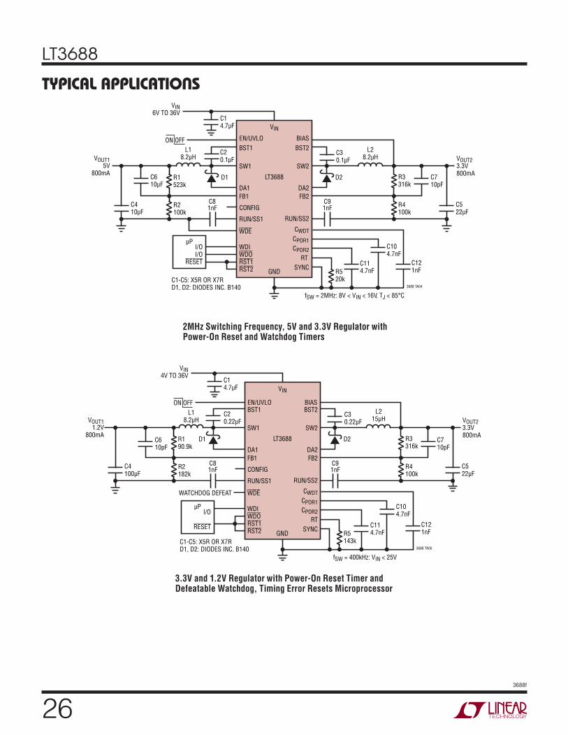
2MHz Switching Frequency, 5V and 3.3V Regulator with Power-On Reset and Watchdog Timers
VIN
LT3688
GND
BIASEN/UVLOBST1
C20.22μF
ON OFF
C14.7μF
VOUT11.2V
800mA
VIN4V TO 36V
C4100μF
L18.2μH
L215μH
R190.9k
R2182k
R3316k
R4100k
C81nF
C91nF
μP
C30.22μF
SW1
DA1
D2D1
BST2
SW2
DA2
FB1
RUN/SS1
WDE
WDIWDO
RST1
RST2
I/O
RESET
FB2
RUN/SS2
CWDT
CPOR1
CPOR2
RT
SYNC
C522μF
C710pF
C121nF
3688 TA05
C104.7nF
C114.7nFR5
143kC1-C5: X5R OR X7RD1, D2: DIODES INC. B140
fSW = 400kHz: VIN < 25V
VOUT23.3V800mA
WATCHDOG DEFEAT
C610pF
CONFIG
3.3V and 1.2V Regulator with Power-On Reset Timer and Defeatable Watchdog, Timing Error Resets Microprocessor
LT3688
273688f
FE24 (AA) TSSOP 0208 REV Ø
0.09 – 0.20(.0035 – .0079)
0 – 8
0.25REF
RECOMMENDED SOLDER PAD LAYOUT
0.50 – 0.75(.020 – .030)
4.30 – 4.50*(.169 – .177)
1 3 4 5 6 7 8 9 10 11 12
14 13
7.70 – 7.90*(.303 – .311)
3.25(.128)
2.74(.108)
2021222324 19 18 17 16 15
1.20(.047)MAX
0.05 – 0.15(.002 – .006)
0.65(.0256)
BSC0.195 – 0.30
(.0077 – .0118)TYP
2
2.74(.108)
0.45 0.05
0.65 BSC
4.50 0.10
6.60 0.10
1.05 0.10
3.25(.128)
MILLIMETERS(INCHES) *DIMENSIONS DO NOT INCLUDE MOLD FLASH. MOLD FLASH
SHALL NOT EXCEED 0.150mm (.006") PER SIDE
NOTE:1. CONTROLLING DIMENSION: MILLIMETERS
2. DIMENSIONS ARE IN
3. DRAWING NOT TO SCALE
SEE NOTE 4
4. RECOMMENDED MINIMUM PCB METAL SIZE FOR EXPOSED PAD ATTACHMENT
6.40(.252)BSC
FE Package24-Lead Plastic TSSOP (4.4mm)
(Reference LTC DWG # 05-08-1771 Rev Ø)
Variation AA
PACKAGE DESCRIPTION
Information furnished by Linear Technology Corporation is believed to be accurate and reliable. However, no responsibility is assumed for its use. Linear Technology Corporation makes no representa-tion that the interconnection of its circuits as described herein will not infringe on existing patent rights.
UF Package24-Lead Plastic QFN (4mm × 4mm)
(Reference LTC DWG # 05-08-1697)
4.00 ± 0.10(4 SIDES)
NOTE:1. DRAWING PROPOSED TO BE MADE A JEDEC PACKAGE OUTLINE MO-220 VARIATION (WGGD-X)—TO BE APPROVED2. DRAWING NOT TO SCALE3. ALL DIMENSIONS ARE IN MILLIMETERS4. DIMENSIONS OF EXPOSED PAD ON BOTTOM OF PACKAGE DO NOT INCLUDE MOLD FLASH. MOLD FLASH, IF PRESENT, SHALL NOT EXCEED 0.15mm ON ANY SIDE, IF PRESENT5. EXPOSED PAD SHALL BE SOLDER PLATED6. SHADED AREA IS ONLY A REFERENCE FOR PIN 1 LOCATION ON THE TOP AND BOTTOM OF PACKAGE
PIN 1TOP MARK(NOTE 6)
0.40 ± 0.10
2423
1
2
BOTTOM VIEW—EXPOSED PAD
2.45 ± 0.10(4-SIDES)
0.75 ± 0.05 R = 0.115TYP
0.25 ± 0.05
0.50 BSC
0.200 REF
0.00 – 0.05
(UF24) QFN 0105
RECOMMENDED SOLDER PAD PITCH AND DIMENSIONS
0.70 ±0.05
0.25 ±0.050.50 BSC
2.45 ± 0.05(4 SIDES)3.10 ± 0.05
4.50 ± 0.05
PACKAGEOUTLINE
PIN 1 NOTCHR = 0.20 TYP OR 0.35 × 45° CHAMFER
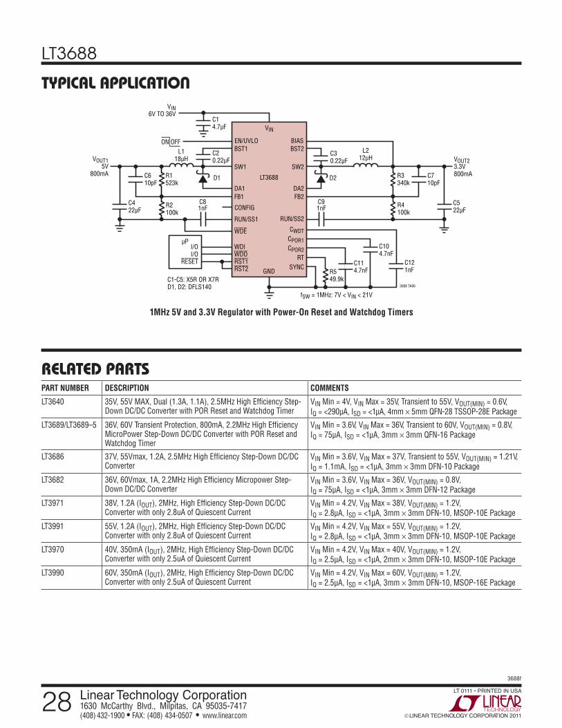
LT3688
283688f
Linear Technology Corporation1630 McCarthy Blvd., Milpitas, CA 95035-7417 (408) 432-1900 ● FAX: (408) 434-0507 ● www.linear.com © LINEAR TECHNOLOGY CORPORATION 2011
LT 0111 • PRINTED IN USA
RELATED PARTSPART NUMBER DESCRIPTION COMMENTS
LT3640 35V, 55V MAX, Dual (1.3A, 1.1A), 2.5MHz High Effi ciency Step-Down DC/DC Converter with POR Reset and Watchdog Timer
VIN Min = 4V, VIN Max = 35V, Transient to 55V, VOUT(MIN) = 0.6V,
IQ = <290μA, ISD = <1μA, 4mm × 5mm QFN-28 TSSOP-28E Package
LT3689/LT3689–5 36V, 60V Transient Protection, 800mA, 2.2MHz High Effi ciency MicroPower Step-Down DC/DC Converter with POR Reset and Watchdog Timer
VIN Min = 3.6V, VIN Max = 36V, Transient to 60V, VOUT(MIN) = 0.8V,
IQ = 75μA, ISD = <1μA, 3mm × 3mm QFN-16 Package
LT3686 37V, 55Vmax, 1.2A, 2.5MHz High Effi ciency Step-Down DC/DC Converter
VIN Min = 3.6V, VIN Max = 37V, Transient to 55V, VOUT(MIN) = 1.21V,
IQ = 1.1mA, ISD = <1μA, 3mm × 3mm DFN-10 Package
LT3682 36V, 60Vmax, 1A, 2.2MHz High Effi ciency Micropower Step-Down DC/DC Converter
VIN Min = 3.6V, VIN Max = 36V, VOUT(MIN) = 0.8V,
IQ = 75μA, ISD = <1μA, 3mm × 3mm DFN-12 Package
LT3971 38V, 1.2A (IOUT), 2MHz, High Effi ciency Step-Down DC/DC Converter with only 2.8uA of Quiescent Current
VIN Min = 4.2V, VIN Max = 38V, VOUT(MIN) = 1.2V,
IQ = 2.8μA, ISD = <1μA, 3mm × 3mm DFN-10, MSOP-10E Package
LT3991 55V, 1.2A (IOUT), 2MHz, High Effi ciency Step-Down DC/DC Converter with only 2.8uA of Quiescent Current
VIN Min = 4.2V, VIN Max = 55V, VOUT(MIN) = 1.2V,
IQ = 2.8μA, ISD = <1μA, 3mm × 3mm DFN-10, MSOP-10E Package
LT3970 40V, 350mA (IOUT), 2MHz, High Effi ciency Step-Down DC/DC Converter with only 2.5uA of Quiescent Current
VIN Min = 4.2V, VIN Max = 40V, VOUT(MIN) = 1.2V,
IQ = 2.5μA, ISD = <1μA, 2mm × 3mm DFN-10, MSOP-10E Package
LT3990 60V, 350mA (IOUT), 2MHz, High Effi ciency Step-Down DC/DC Converter with only 2.5uA of Quiescent Current
VIN Min = 4.2V, VIN Max = 60V, VOUT(MIN) = 1.2V,
IQ = 2.5μA, ISD = <1μA, 3mm × 3mm DFN-10, MSOP-16E Package
TYPICAL APPLICATION
CONFIG
VIN
LT3688
GND
BIASEN/UVLO
BST1C20.22μF
ON OFF
C14.7μF
VOUT15V
800mA
VIN6V TO 36V
C422μF
C610pF
C710pF
L118μH
L212μH
R1523k
R2100k
R3340k
R4100k
C81nF
C91nF
μP
C30.22μF
SW1
DA1
D2D1
BST2
SW2
DA2
FB1
RUN/SS1
WDE
WDIWDO
RST1
RST2
I/OI/O
RESET
FB2
RUN/SS2
CWDT
CPOR1
CPOR2
RT
SYNC
C522μF
C121nF
3688 TA06
C104.7nF
C114.7nFR5
49.9kC1-C5: X5R OR X7RD1, D2: DFLS140
fSW = 1MHz: 7V < VIN < 21V
VOUT23.3V800mA
1MHz 5V and 3.3V Regulator with Power-On Reset and Watchdog Timers
![Timsirin n Tirra [ILUGAN N TIRRA]](https://static.fdocument.org/doc/165x107/55cf991c550346d0339ba273/timsirin-n-tirra-ilugan-n-tirra.jpg)