LF444 Quad Low Power JFET Input Operational Amplifier · PDF fileLF444 SNOSC04D – MAY...
18
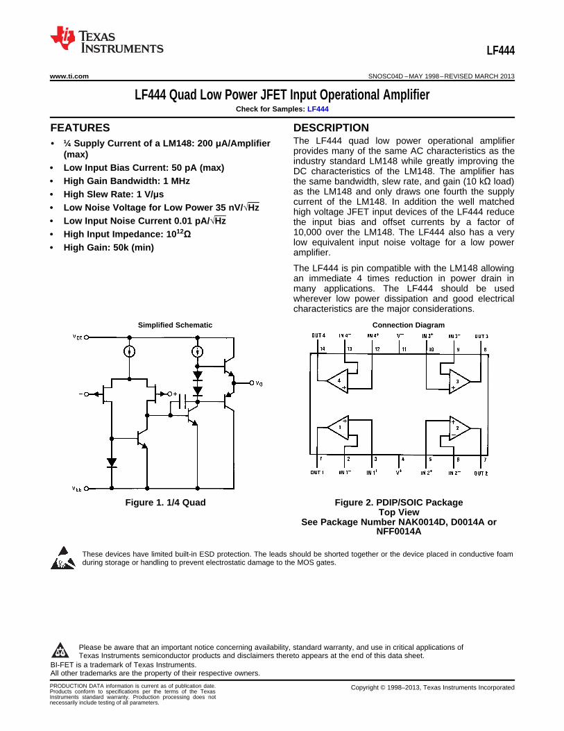
LF444 www.ti.com SNOSC04D – MAY 1998 – REVISED MARCH 2013 LF444 Quad Low Power JFET Input Operational Amplifier Check for Samples: LF444 1FEATURES DESCRIPTION The LF444 quad low power operational amplifier 23• ¼ Supply Current of a LM148: 200 μA/Amplifier provides many of the same AC characteristics as the (max) industry standard LM148 while greatly improving the • Low Input Bias Current: 50 pA (max) DC characteristics of the LM148. The amplifier has • High Gain Bandwidth: 1 MHz the same bandwidth, slew rate, and gain (10 kΩ load) as the LM148 and only draws one fourth the supply • High Slew Rate: 1 V/μs current of the LM148. In addition the well matched • Low Noise Voltage for Low Power 35 nV/√Hz high voltage JFET input devices of the LF444 reduce • Low Input Noise Current 0.01 pA/√Hz the input bias and offset currents by a factor of 10,000 over the LM148. The LF444 also has a very • High Input Impedance: 10 12 Ω low equivalent input noise voltage for a low power • High Gain: 50k (min) amplifier. The LF444 is pin compatible with the LM148 allowing an immediate 4 times reduction in power drain in many applications. The LF444 should be used wherever low power dissipation and good electrical characteristics are the major considerations. Simplified Schematic Connection Diagram Figure 1. 1/4 Quad Figure 2. PDIP/SOIC Package Top View See Package Number NAK0014D, D0014A or NFF0014A These devices have limited built-in ESD protection. The leads should be shorted together or the device placed in conductive foam during storage or handling to prevent electrostatic damage to the MOS gates. 1 Please be aware that an important notice concerning availability, standard warranty, and use in critical applications of Texas Instruments semiconductor products and disclaimers thereto appears at the end of this data sheet. 2BI-FET is a trademark of Texas Instruments. 3All other trademarks are the property of their respective owners. PRODUCTION DATA information is current as of publication date. Copyright © 1998–2013, Texas Instruments Incorporated Products conform to specifications per the terms of the Texas Instruments standard warranty. Production processing does not necessarily include testing of all parameters.
Transcript of LF444 Quad Low Power JFET Input Operational Amplifier · PDF fileLF444 SNOSC04D – MAY...
LF444
www.ti.com SNOSC04D –MAY 1998–REVISED MARCH 2013
LF444 Quad Low Power JFET Input Operational AmplifierCheck for Samples: LF444
1FEATURES DESCRIPTIONThe LF444 quad low power operational amplifier
23• ¼ Supply Current of a LM148: 200 μA/Amplifierprovides many of the same AC characteristics as the(max)industry standard LM148 while greatly improving the
• Low Input Bias Current: 50 pA (max) DC characteristics of the LM148. The amplifier has• High Gain Bandwidth: 1 MHz the same bandwidth, slew rate, and gain (10 kΩ load)
as the LM148 and only draws one fourth the supply• High Slew Rate: 1 V/μscurrent of the LM148. In addition the well matched
• Low Noise Voltage for Low Power 35 nV/√Hz high voltage JFET input devices of the LF444 reduce• Low Input Noise Current 0.01 pA/√Hz the input bias and offset currents by a factor of
10,000 over the LM148. The LF444 also has a very• High Input Impedance: 1012Ωlow equivalent input noise voltage for a low power• High Gain: 50k (min) amplifier.
The LF444 is pin compatible with the LM148 allowingan immediate 4 times reduction in power drain inmany applications. The LF444 should be usedwherever low power dissipation and good electricalcharacteristics are the major considerations.
Simplified Schematic Connection Diagram
Figure 1. 1/4 Quad Figure 2. PDIP/SOIC PackageTop View
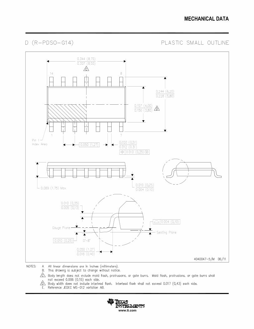
See Package Number NAK0014D, D0014A orNFF0014A
These devices have limited built-in ESD protection. The leads should be shorted together or the device placed in conductive foamduring storage or handling to prevent electrostatic damage to the MOS gates.
1
Please be aware that an important notice concerning availability, standard warranty, and use in critical applications ofTexas Instruments semiconductor products and disclaimers thereto appears at the end of this data sheet.
2BI-FET is a trademark of Texas Instruments.3All other trademarks are the property of their respective owners.
PRODUCTION DATA information is current as of publication date. Copyright © 1998–2013, Texas Instruments IncorporatedProducts conform to specifications per the terms of the TexasInstruments standard warranty. Production processing does notnecessarily include testing of all parameters.
LF444
SNOSC04D –MAY 1998–REVISED MARCH 2013 www.ti.com
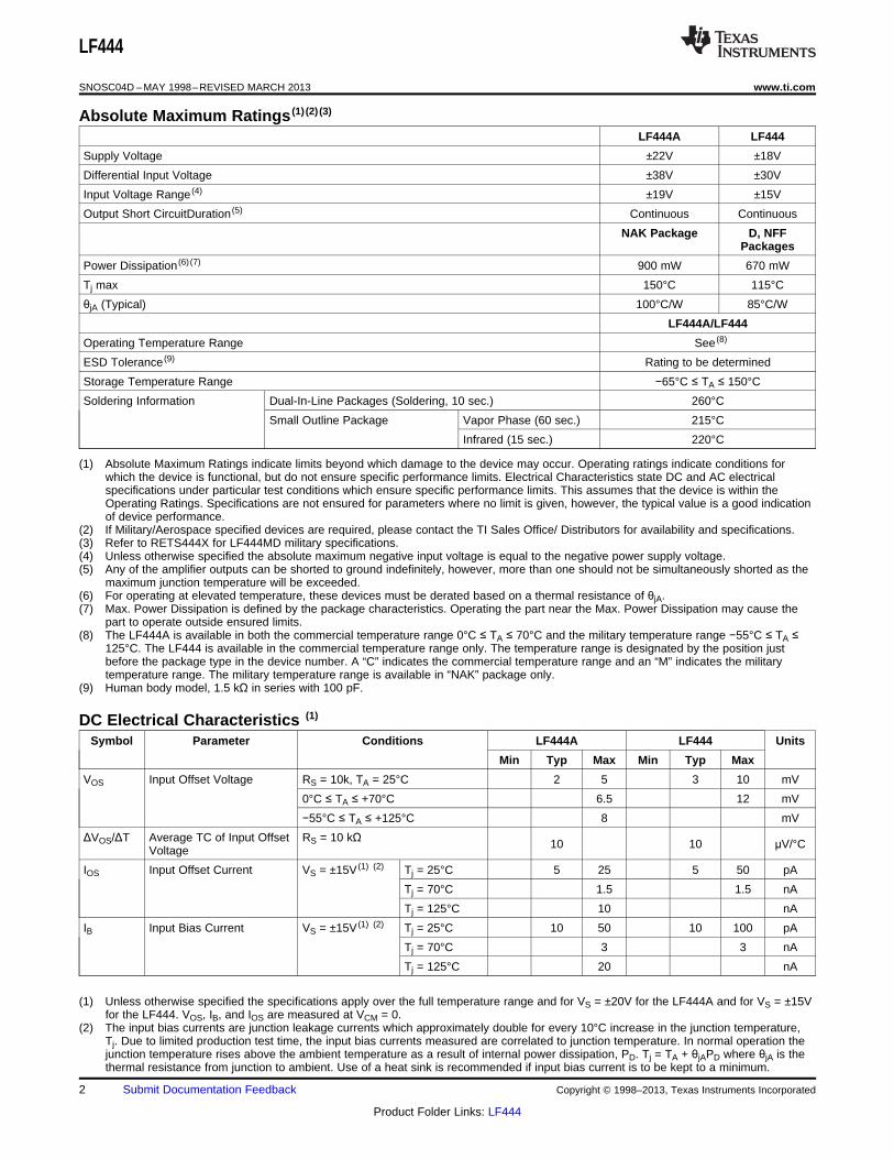
Absolute Maximum Ratings (1) (2) (3)
LF444A LF444
Supply Voltage ±22V ±18V
Differential Input Voltage ±38V ±30V
Input Voltage Range (4) ±19V ±15V
Output Short CircuitDuration (5) Continuous Continuous
NAK Package D, NFFPackages
Power Dissipation (6) (7) 900 mW 670 mW
Tj max 150°C 115°C
θjA (Typical) 100°C/W 85°C/W
LF444A/LF444
Operating Temperature Range See (8)
ESD Tolerance (9) Rating to be determined
Storage Temperature Range −65°C ≤ TA ≤ 150°C
Soldering Information Dual-In-Line Packages (Soldering, 10 sec.) 260°C
Small Outline Package Vapor Phase (60 sec.) 215°C
Infrared (15 sec.) 220°C
(1) Absolute Maximum Ratings indicate limits beyond which damage to the device may occur. Operating ratings indicate conditions forwhich the device is functional, but do not ensure specific performance limits. Electrical Characteristics state DC and AC electricalspecifications under particular test conditions which ensure specific performance limits. This assumes that the device is within theOperating Ratings. Specifications are not ensured for parameters where no limit is given, however, the typical value is a good indicationof device performance.
(2) If Military/Aerospace specified devices are required, please contact the TI Sales Office/ Distributors for availability and specifications.(3) Refer to RETS444X for LF444MD military specifications.(4) Unless otherwise specified the absolute maximum negative input voltage is equal to the negative power supply voltage.(5) Any of the amplifier outputs can be shorted to ground indefinitely, however, more than one should not be simultaneously shorted as the
maximum junction temperature will be exceeded.(6) For operating at elevated temperature, these devices must be derated based on a thermal resistance of θjA.(7) Max. Power Dissipation is defined by the package characteristics. Operating the part near the Max. Power Dissipation may cause the
part to operate outside ensured limits.(8) The LF444A is available in both the commercial temperature range 0°C ≤ TA ≤ 70°C and the military temperature range −55°C ≤ TA ≤
125°C. The LF444 is available in the commercial temperature range only. The temperature range is designated by the position justbefore the package type in the device number. A “C” indicates the commercial temperature range and an “M” indicates the militarytemperature range. The military temperature range is available in “NAK” package only.
(9) Human body model, 1.5 kΩ in series with 100 pF.
DC Electrical Characteristics (1)
Symbol Parameter Conditions LF444A LF444 Units
Min Typ Max Min Typ Max
VOS Input Offset Voltage RS = 10k, TA = 25°C 2 5 3 10 mV
0°C ≤ TA ≤ +70°C 6.5 12 mV
−55°C ≤ TA ≤ +125°C 8 mV
ΔVOS/ΔT Average TC of Input Offset RS = 10 kΩ 10 10 μV/°CVoltage
IOS Input Offset Current VS = ±15V (1) (2) Tj = 25°C 5 25 5 50 pA
Tj = 70°C 1.5 1.5 nA
Tj = 125°C 10 nA
IB Input Bias Current VS = ±15V (1) (2) Tj = 25°C 10 50 10 100 pA
Tj = 70°C 3 3 nA
Tj = 125°C 20 nA
(1) Unless otherwise specified the specifications apply over the full temperature range and for VS = ±20V for the LF444A and for VS = ±15Vfor the LF444. VOS, IB, and IOS are measured at VCM = 0.
(2) The input bias currents are junction leakage currents which approximately double for every 10°C increase in the junction temperature,Tj. Due to limited production test time, the input bias currents measured are correlated to junction temperature. In normal operation thejunction temperature rises above the ambient temperature as a result of internal power dissipation, PD. Tj = TA + θjAPD where θjA is thethermal resistance from junction to ambient. Use of a heat sink is recommended if input bias current is to be kept to a minimum.
2 Submit Documentation Feedback Copyright © 1998–2013, Texas Instruments Incorporated
Product Folder Links: LF444
LF444
www.ti.com SNOSC04D –MAY 1998–REVISED MARCH 2013
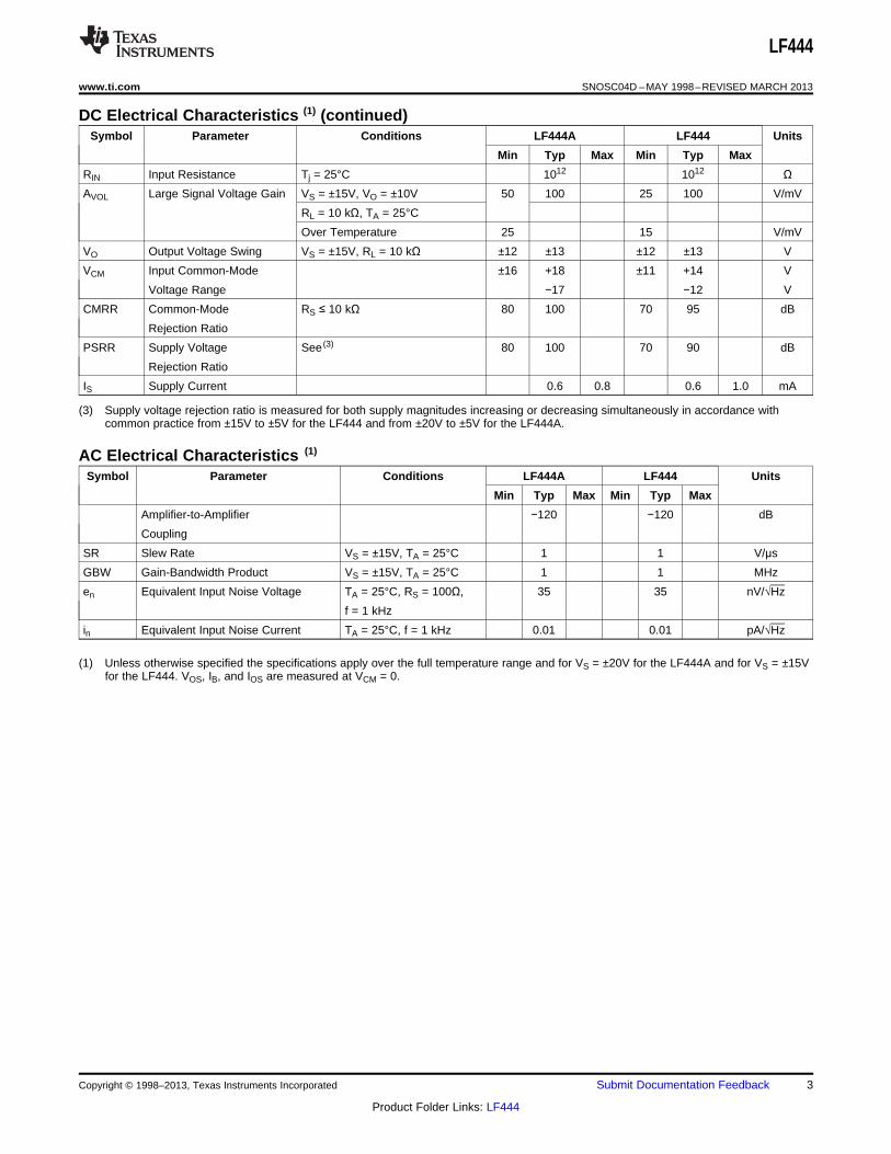
DC Electrical Characteristics (1) (continued)Symbol Parameter Conditions LF444A LF444 Units
Min Typ Max Min Typ Max
RIN Input Resistance Tj = 25°C 1012 1012 ΩAVOL Large Signal Voltage Gain VS = ±15V, VO = ±10V 50 100 25 100 V/mV
RL = 10 kΩ, TA = 25°C
Over Temperature 25 15 V/mV
VO Output Voltage Swing VS = ±15V, RL = 10 kΩ ±12 ±13 ±12 ±13 V
VCM Input Common-Mode ±16 +18 ±11 +14 V
Voltage Range −17 −12 V
CMRR Common-Mode RS ≤ 10 kΩ 80 100 70 95 dB
Rejection Ratio
PSRR Supply Voltage See (3) 80 100 70 90 dB
Rejection Ratio
IS Supply Current 0.6 0.8 0.6 1.0 mA
(3) Supply voltage rejection ratio is measured for both supply magnitudes increasing or decreasing simultaneously in accordance withcommon practice from ±15V to ±5V for the LF444 and from ±20V to ±5V for the LF444A.
AC Electrical Characteristics (1)
Symbol Parameter Conditions LF444A LF444 Units
Min Typ Max Min Typ Max
Amplifier-to-Amplifier −120 −120 dB
Coupling
SR Slew Rate VS = ±15V, TA = 25°C 1 1 V/μs
GBW Gain-Bandwidth Product VS = ±15V, TA = 25°C 1 1 MHz
en Equivalent Input Noise Voltage TA = 25°C, RS = 100Ω, 35 35 nV/√Hz
f = 1 kHz
in Equivalent Input Noise Current TA = 25°C, f = 1 kHz 0.01 0.01 pA/√Hz
(1) Unless otherwise specified the specifications apply over the full temperature range and for VS = ±20V for the LF444A and for VS = ±15Vfor the LF444. VOS, IB, and IOS are measured at VCM = 0.
Copyright © 1998–2013, Texas Instruments Incorporated Submit Documentation Feedback 3
Product Folder Links: LF444
LF444
SNOSC04D –MAY 1998–REVISED MARCH 2013 www.ti.com
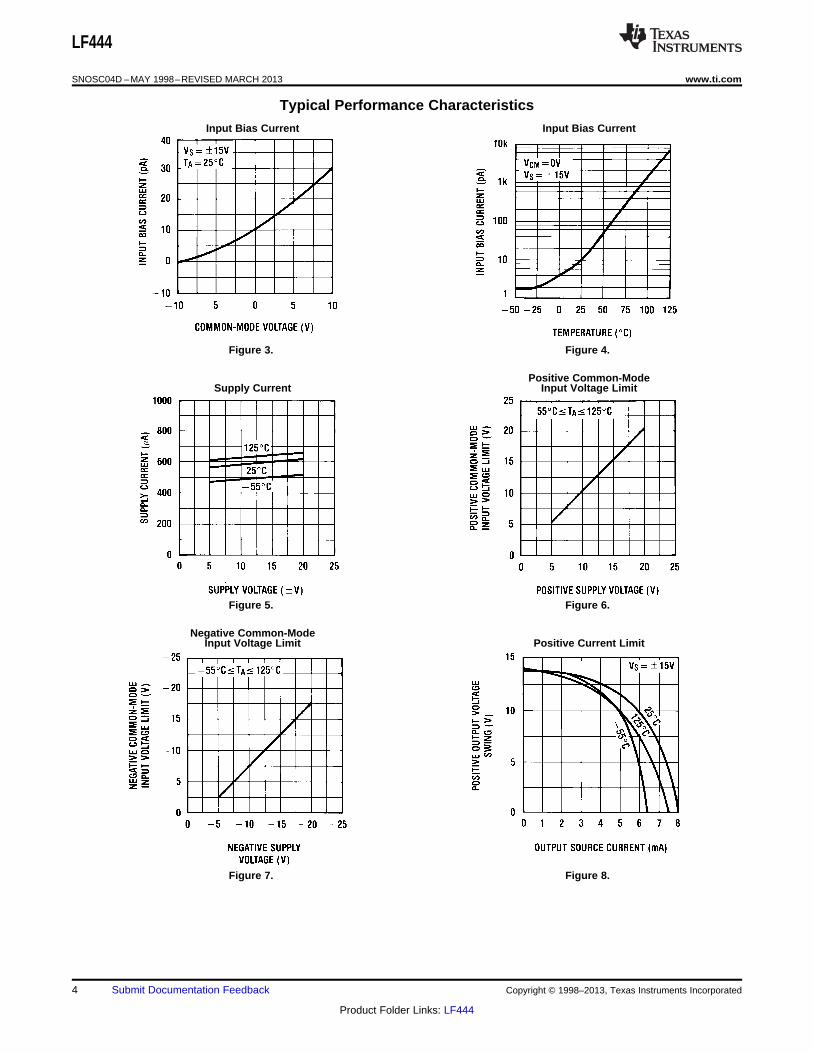
Typical Performance Characteristics
Input Bias Current Input Bias Current
Figure 3. Figure 4.
Positive Common-ModeSupply Current Input Voltage Limit
Figure 5. Figure 6.
Negative Common-ModeInput Voltage Limit Positive Current Limit
Figure 7. Figure 8.
4 Submit Documentation Feedback Copyright © 1998–2013, Texas Instruments Incorporated
Product Folder Links: LF444
LF444
www.ti.com SNOSC04D –MAY 1998–REVISED MARCH 2013
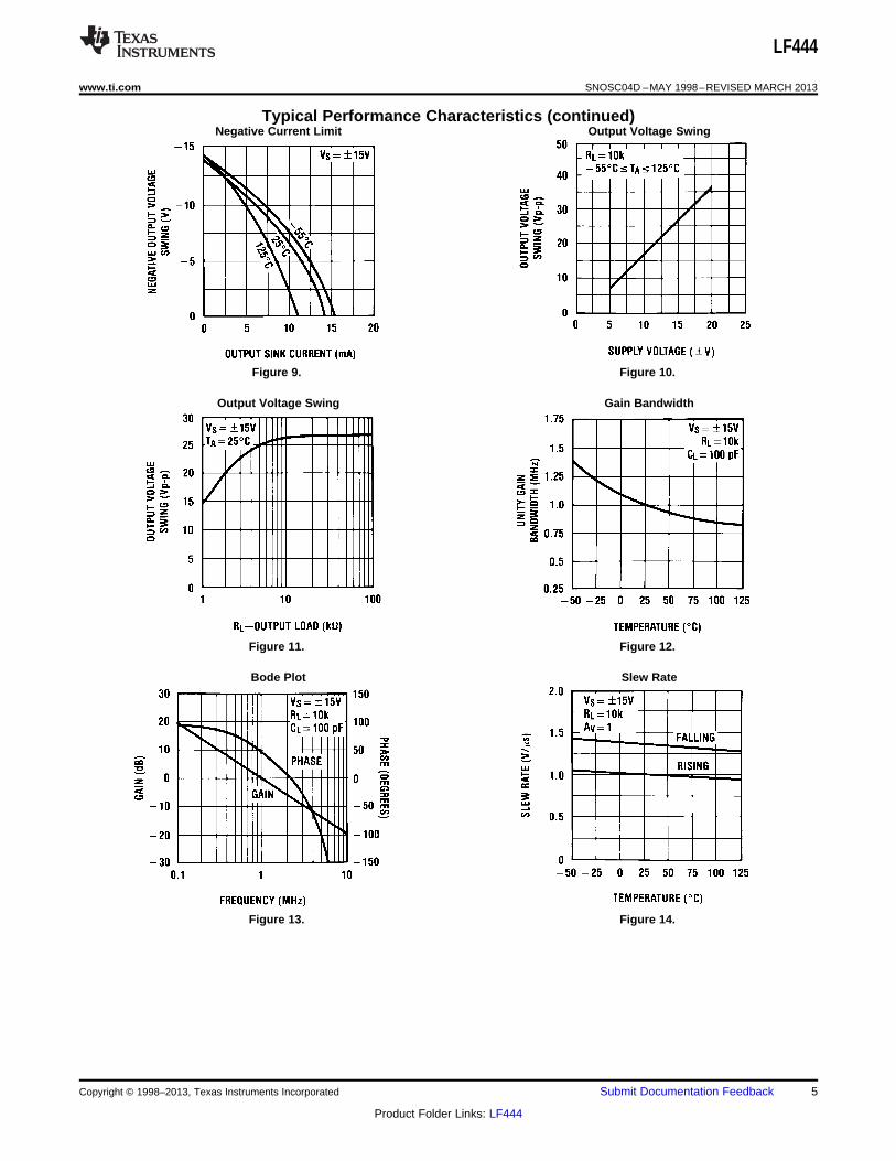
Typical Performance Characteristics (continued)Negative Current Limit Output Voltage Swing
Figure 9. Figure 10.
Output Voltage Swing Gain Bandwidth
Figure 11. Figure 12.
Bode Plot Slew Rate
Figure 13. Figure 14.
Copyright © 1998–2013, Texas Instruments Incorporated Submit Documentation Feedback 5
Product Folder Links: LF444
LF444
SNOSC04D –MAY 1998–REVISED MARCH 2013 www.ti.com
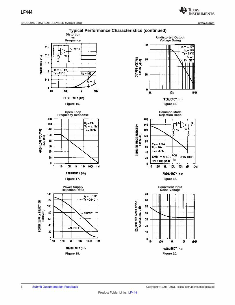
Typical Performance Characteristics (continued)Distortion
vs Undistorted OutputFrequency Voltage Swing
Figure 15. Figure 16.
Open Loop Common-ModeFrequency Response Rejection Ratio
Figure 17. Figure 18.
Power Supply Equivalent InputRejection Ratio Noise Voltage
Figure 19. Figure 20.
6 Submit Documentation Feedback Copyright © 1998–2013, Texas Instruments Incorporated
Product Folder Links: LF444
LF444
www.ti.com SNOSC04D –MAY 1998–REVISED MARCH 2013
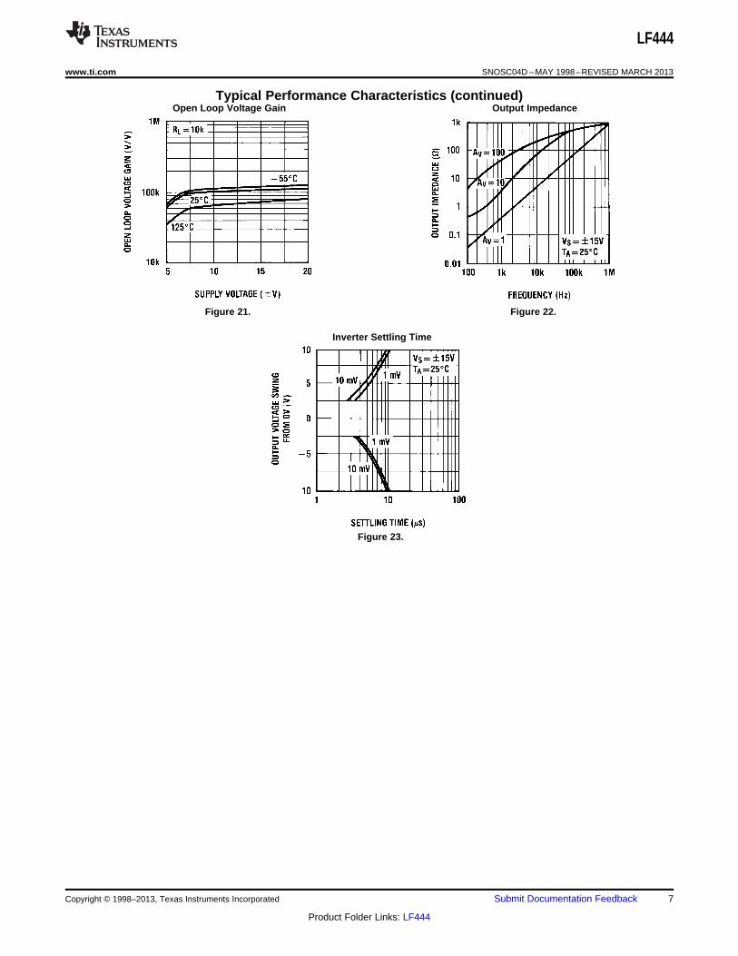
Typical Performance Characteristics (continued)Open Loop Voltage Gain Output Impedance
Figure 21. Figure 22.
Inverter Settling Time
Figure 23.
Copyright © 1998–2013, Texas Instruments Incorporated Submit Documentation Feedback 7
Product Folder Links: LF444
LF444
SNOSC04D –MAY 1998–REVISED MARCH 2013 www.ti.com
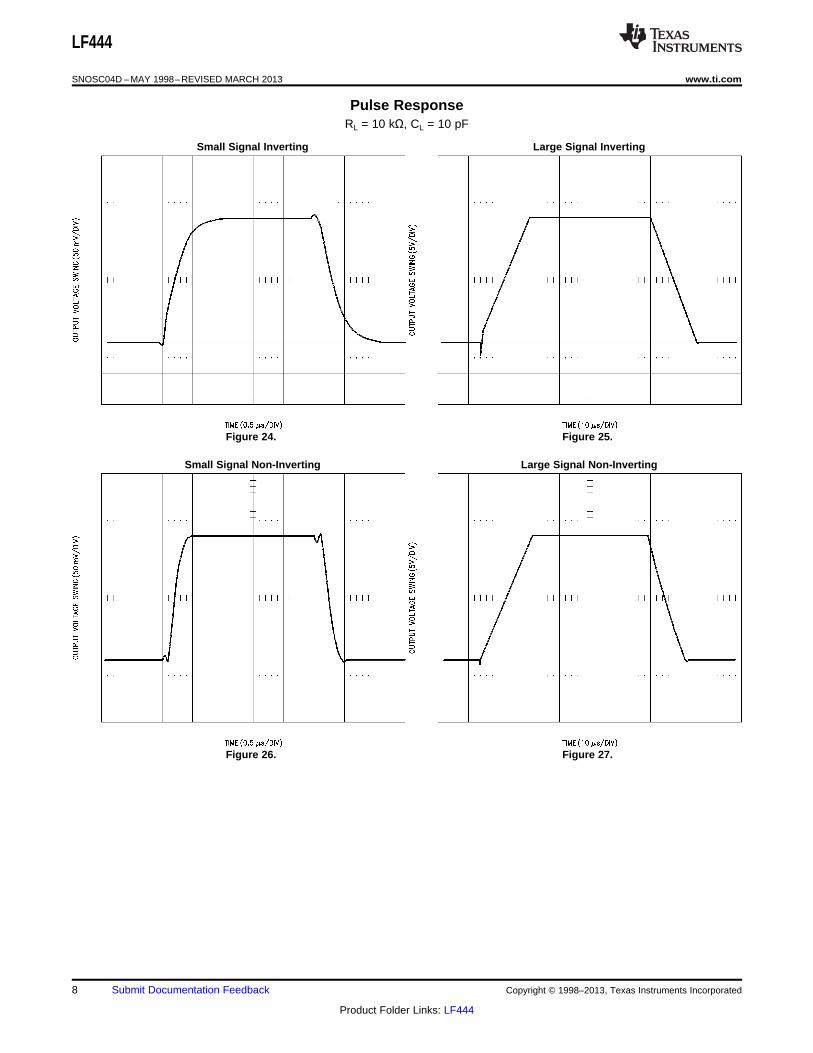
Pulse ResponseRL = 10 kΩ, CL = 10 pF
Small Signal Inverting Large Signal Inverting
Figure 24. Figure 25.
Small Signal Non-Inverting Large Signal Non-Inverting
Figure 26. Figure 27.
8 Submit Documentation Feedback Copyright © 1998–2013, Texas Instruments Incorporated
Product Folder Links: LF444
LF444
www.ti.com SNOSC04D –MAY 1998–REVISED MARCH 2013
APPLICATION HINTS
This device is a quad low power op amp with JFET input devices ( BI-FET™). These JFETs have large reversebreakdown voltages from gate to source and drain eliminating the need for clamps across the inputs. Therefore,large differential input voltages can easily be accommodated without a large increase in input current. Themaximum differential input voltage is independent of the supply voltages. However, neither of the input voltagesshould be allowed to exceed the negative supply as this will cause large currents to flow which can result in adestroyed unit.
Exceeding the negative common-mode limit on either input will force the output to a high state, potentiallycausing a reversal of phase to the output. Exceeding the negative common-mode limit on both inputs will forcethe amplifier output to a high state. In neither case does a latch occur since raising the input back within thecommon-mode range again puts the input stage and thus the amplifier in a normal operating mode.
Exceeding the positive common-mode limit on a single input will not change the phase of the output; however, ifboth inputs exceed the limit, the output of the amplifier will be forced to a high state.
The amplifiers will operate with a common-mode input voltage equal to the positive supply; however, the gainbandwidth and slew rate may be decreased in this condition. When the negative common-mode voltage swingsto within 3V of the negative supply, an increase in input offset voltage may occur.
Each amplifier is individually biased to allow normal circuit operation with power supplies of ±3.0V. Supplyvoltages less than these may degrade the common-mode rejection and restrict the output voltage swing.
The amplifiers will drive a 10 kΩ load resistance to ±10V over the full temperature range. If the amplifier is forcedto drive heavier load currents, however, an increase in input offset voltage may occur on the negative voltageswing and finally reach an active current limit on both positive and negative swings.
Precautions should be taken to ensure that the power supply for the integrated circuit never becomes reversed inpolarity or that the unit is not inadvertently installed backwards in a socket as an unlimited current surge throughthe resulting forward diode within the IC could cause fusing of the internal conductors and result in a destroyedunit.
As with most amplifiers, care should be taken with lead dress, component placement and supply decoupling inorder to ensure stability. For example, resistors from the output to an input should be placed with the body closeto the input to minimize “pick-up” and maximize the frequency of the feedback pole by minimizing thecapacitance from the input to ground.
A feedback pole is created when the feedback around any amplifier is resistive. The parallel resistance andcapacitance from the input of the device (usually the inverting input) to AC ground set the frequency of the pole.In many instances the frequency of this pole is much greater than the expected 3 dB frequency of the closedloop gain and consequently there is negligible effect on stability margin. However, if the feedback pole is lessthan approximately 6 times the expected 3 dB frequency a lead capacitor should be placed from the output to theinput of the op amp. The value of the added capacitor should be such that the RC time constant of this capacitorand the resistance it parallels is greater than or equal to the original feedback pole time constant.
Copyright © 1998–2013, Texas Instruments Incorporated Submit Documentation Feedback 9
Product Folder Links: LF444
LF444
SNOSC04D –MAY 1998–REVISED MARCH 2013 www.ti.com
Typical Application
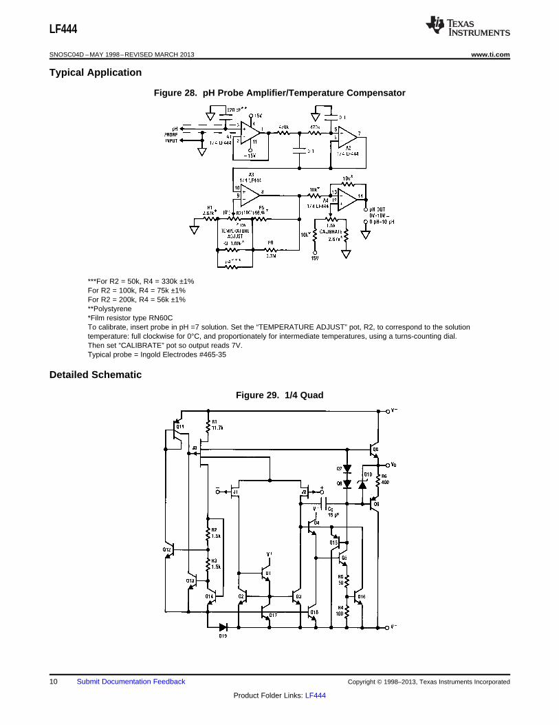
Figure 28. pH Probe Amplifier/Temperature Compensator
***For R2 = 50k, R4 = 330k ±1%For R2 = 100k, R4 = 75k ±1%For R2 = 200k, R4 = 56k ±1%**Polystyrene*Film resistor type RN60CTo calibrate, insert probe in pH =7 solution. Set the “TEMPERATURE ADJUST” pot, R2, to correspond to the solutiontemperature: full clockwise for 0°C, and proportionately for intermediate temperatures, using a turns-counting dial.Then set “CALIBRATE” pot so output reads 7V.Typical probe = Ingold Electrodes #465-35
Detailed Schematic
Figure 29. 1/4 Quad
10 Submit Documentation Feedback Copyright © 1998–2013, Texas Instruments Incorporated
Product Folder Links: LF444
LF444
www.ti.com SNOSC04D –MAY 1998–REVISED MARCH 2013
REVISION HISTORY
Changes from Revision C (March 2013) to Revision D Page
• Changed layout of National Data Sheet to TI format .......................................................................................................... 10
Copyright © 1998–2013, Texas Instruments Incorporated Submit Documentation Feedback 11
Product Folder Links: LF444
PACKAGE OPTION ADDENDUM
www.ti.com 21-Mar-2015
Addendum-Page 1
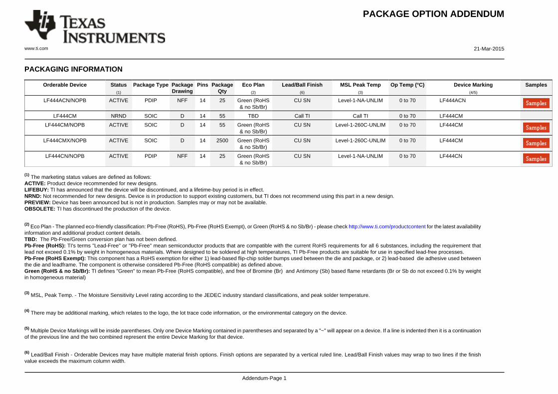
PACKAGING INFORMATION
Orderable Device Status(1)
Package Type PackageDrawing
Pins PackageQty
Eco Plan(2)
Lead/Ball Finish(6)
MSL Peak Temp(3)
Op Temp (°C) Device Marking(4/5)
Samples
LF444ACN/NOPB ACTIVE PDIP NFF 14 25 Green (RoHS& no Sb/Br)
CU SN Level-1-NA-UNLIM 0 to 70 LF444ACN
LF444CM NRND SOIC D 14 55 TBD Call TI Call TI 0 to 70 LF444CM
LF444CM/NOPB ACTIVE SOIC D 14 55 Green (RoHS& no Sb/Br)
CU SN Level-1-260C-UNLIM 0 to 70 LF444CM
LF444CMX/NOPB ACTIVE SOIC D 14 2500 Green (RoHS& no Sb/Br)
CU SN Level-1-260C-UNLIM 0 to 70 LF444CM
LF444CN/NOPB ACTIVE PDIP NFF 14 25 Green (RoHS& no Sb/Br)
CU SN Level-1-NA-UNLIM 0 to 70 LF444CN
(1) The marketing status values are defined as follows:ACTIVE: Product device recommended for new designs.LIFEBUY: TI has announced that the device will be discontinued, and a lifetime-buy period is in effect.NRND: Not recommended for new designs. Device is in production to support existing customers, but TI does not recommend using this part in a new design.PREVIEW: Device has been announced but is not in production. Samples may or may not be available.OBSOLETE: TI has discontinued the production of the device.
(2) Eco Plan - The planned eco-friendly classification: Pb-Free (RoHS), Pb-Free (RoHS Exempt), or Green (RoHS & no Sb/Br) - please check http://www.ti.com/productcontent for the latest availabilityinformation and additional product content details.TBD: The Pb-Free/Green conversion plan has not been defined.Pb-Free (RoHS): TI's terms "Lead-Free" or "Pb-Free" mean semiconductor products that are compatible with the current RoHS requirements for all 6 substances, including the requirement thatlead not exceed 0.1% by weight in homogeneous materials. Where designed to be soldered at high temperatures, TI Pb-Free products are suitable for use in specified lead-free processes.Pb-Free (RoHS Exempt): This component has a RoHS exemption for either 1) lead-based flip-chip solder bumps used between the die and package, or 2) lead-based die adhesive used betweenthe die and leadframe. The component is otherwise considered Pb-Free (RoHS compatible) as defined above.Green (RoHS & no Sb/Br): TI defines "Green" to mean Pb-Free (RoHS compatible), and free of Bromine (Br) and Antimony (Sb) based flame retardants (Br or Sb do not exceed 0.1% by weightin homogeneous material)
(3) MSL, Peak Temp. - The Moisture Sensitivity Level rating according to the JEDEC industry standard classifications, and peak solder temperature.
(4) There may be additional marking, which relates to the logo, the lot trace code information, or the environmental category on the device.
(5) Multiple Device Markings will be inside parentheses. Only one Device Marking contained in parentheses and separated by a "~" will appear on a device. If a line is indented then it is a continuationof the previous line and the two combined represent the entire Device Marking for that device.
(6) Lead/Ball Finish - Orderable Devices may have multiple material finish options. Finish options are separated by a vertical ruled line. Lead/Ball Finish values may wrap to two lines if the finishvalue exceeds the maximum column width.
PACKAGE OPTION ADDENDUM
www.ti.com 21-Mar-2015
Addendum-Page 2
Important Information and Disclaimer:The information provided on this page represents TI's knowledge and belief as of the date that it is provided. TI bases its knowledge and belief on informationprovided by third parties, and makes no representation or warranty as to the accuracy of such information. Efforts are underway to better integrate information from third parties. TI has taken andcontinues to take reasonable steps to provide representative and accurate information but may not have conducted destructive testing or chemical analysis on incoming materials and chemicals.TI and TI suppliers consider certain information to be proprietary, and thus CAS numbers and other limited information may not be available for release.
In no event shall TI's liability arising out of such information exceed the total purchase price of the TI part(s) at issue in this document sold by TI to Customer on an annual basis.
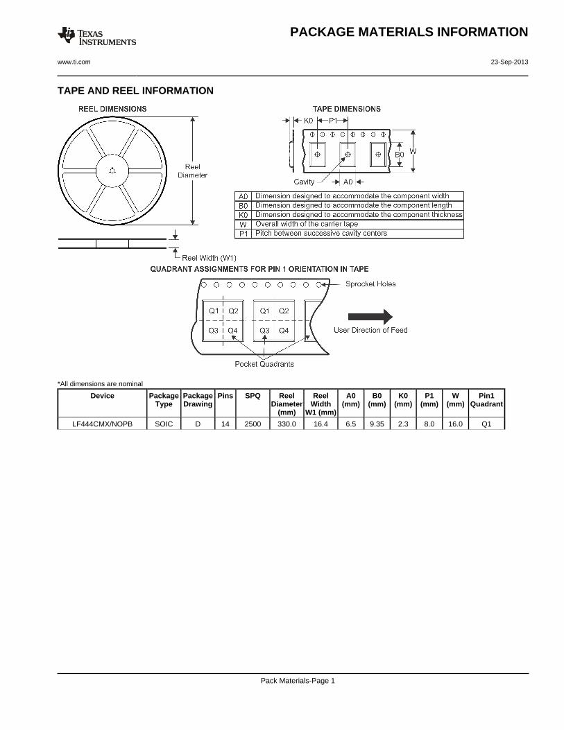
TAPE AND REEL INFORMATION
*All dimensions are nominal
Device PackageType
PackageDrawing
Pins SPQ ReelDiameter
(mm)
ReelWidth
W1 (mm)
A0(mm)
B0(mm)
K0(mm)
P1(mm)
W(mm)
Pin1Quadrant
LF444CMX/NOPB SOIC D 14 2500 330.0 16.4 6.5 9.35 2.3 8.0 16.0 Q1
PACKAGE MATERIALS INFORMATION
www.ti.com 23-Sep-2013
Pack Materials-Page 1
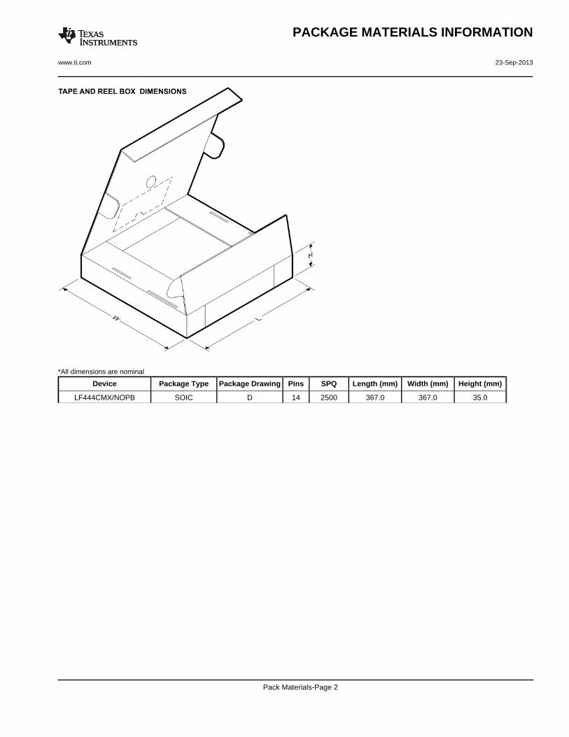
*All dimensions are nominal
Device Package Type Package Drawing Pins SPQ Length (mm) Width (mm) Height (mm)
LF444CMX/NOPB SOIC D 14 2500 367.0 367.0 35.0
PACKAGE MATERIALS INFORMATION
www.ti.com 23-Sep-2013
Pack Materials-Page 2
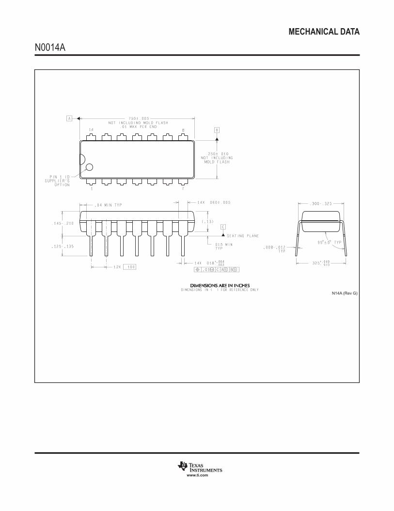
MECHANICAL DATA
N0014A
www.ti.com
N14A (Rev G)
a0412025
Text Box
NFF0014A
IMPORTANT NOTICE
Texas Instruments Incorporated and its subsidiaries (TI) reserve the right to make corrections, enhancements, improvements and otherchanges to its semiconductor products and services per JESD46, latest issue, and to discontinue any product or service per JESD48, latestissue. Buyers should obtain the latest relevant information before placing orders and should verify that such information is current andcomplete. All semiconductor products (also referred to herein as “components”) are sold subject to TI’s terms and conditions of salesupplied at the time of order acknowledgment.TI warrants performance of its components to the specifications applicable at the time of sale, in accordance with the warranty in TI’s termsand conditions of sale of semiconductor products. Testing and other quality control techniques are used to the extent TI deems necessaryto support this warranty. Except where mandated by applicable law, testing of all parameters of each component is not necessarilyperformed.TI assumes no liability for applications assistance or the design of Buyers’ products. Buyers are responsible for their products andapplications using TI components. To minimize the risks associated with Buyers’ products and applications, Buyers should provideadequate design and operating safeguards.TI does not warrant or represent that any license, either express or implied, is granted under any patent right, copyright, mask work right, orother intellectual property right relating to any combination, machine, or process in which TI components or services are used. Informationpublished by TI regarding third-party products or services does not constitute a license to use such products or services or a warranty orendorsement thereof. Use of such information may require a license from a third party under the patents or other intellectual property of thethird party, or a license from TI under the patents or other intellectual property of TI.Reproduction of significant portions of TI information in TI data books or data sheets is permissible only if reproduction is without alterationand is accompanied by all associated warranties, conditions, limitations, and notices. TI is not responsible or liable for such altereddocumentation. Information of third parties may be subject to additional restrictions.Resale of TI components or services with statements different from or beyond the parameters stated by TI for that component or servicevoids all express and any implied warranties for the associated TI component or service and is an unfair and deceptive business practice.TI is not responsible or liable for any such statements.Buyer acknowledges and agrees that it is solely responsible for compliance with all legal, regulatory and safety-related requirementsconcerning its products, and any use of TI components in its applications, notwithstanding any applications-related information or supportthat may be provided by TI. Buyer represents and agrees that it has all the necessary expertise to create and implement safeguards whichanticipate dangerous consequences of failures, monitor failures and their consequences, lessen the likelihood of failures that might causeharm and take appropriate remedial actions. Buyer will fully indemnify TI and its representatives against any damages arising out of the useof any TI components in safety-critical applications.In some cases, TI components may be promoted specifically to facilitate safety-related applications. With such components, TI’s goal is tohelp enable customers to design and create their own end-product solutions that meet applicable functional safety standards andrequirements. Nonetheless, such components are subject to these terms.No TI components are authorized for use in FDA Class III (or similar life-critical medical equipment) unless authorized officers of the partieshave executed a special agreement specifically governing such use.Only those TI components which TI has specifically designated as military grade or “enhanced plastic” are designed and intended for use inmilitary/aerospace applications or environments. Buyer acknowledges and agrees that any military or aerospace use of TI componentswhich have not been so designated is solely at the Buyer's risk, and that Buyer is solely responsible for compliance with all legal andregulatory requirements in connection with such use.TI has specifically designated certain components as meeting ISO/TS16949 requirements, mainly for automotive use. In any case of use ofnon-designated products, TI will not be responsible for any failure to meet ISO/TS16949.
Products ApplicationsAudio www.ti.com/audio Automotive and Transportation www.ti.com/automotiveAmplifiers amplifier.ti.com Communications and Telecom www.ti.com/communicationsData Converters dataconverter.ti.com Computers and Peripherals www.ti.com/computersDLP® Products www.dlp.com Consumer Electronics www.ti.com/consumer-appsDSP dsp.ti.com Energy and Lighting www.ti.com/energyClocks and Timers www.ti.com/clocks Industrial www.ti.com/industrialInterface interface.ti.com Medical www.ti.com/medicalLogic logic.ti.com Security www.ti.com/securityPower Mgmt power.ti.com Space, Avionics and Defense www.ti.com/space-avionics-defenseMicrocontrollers microcontroller.ti.com Video and Imaging www.ti.com/videoRFID www.ti-rfid.comOMAP Applications Processors www.ti.com/omap TI E2E Community e2e.ti.comWireless Connectivity www.ti.com/wirelessconnectivity
Mailing Address: Texas Instruments, Post Office Box 655303, Dallas, Texas 75265Copyright © 2015, Texas Instruments Incorporated