
Lecture 15 Small AC Signal Analysis of...
26
Lecture 15 Small AC Signal Analysis of BJT BJT 1-1
Transcript of Lecture 15 Small AC Signal Analysis of...
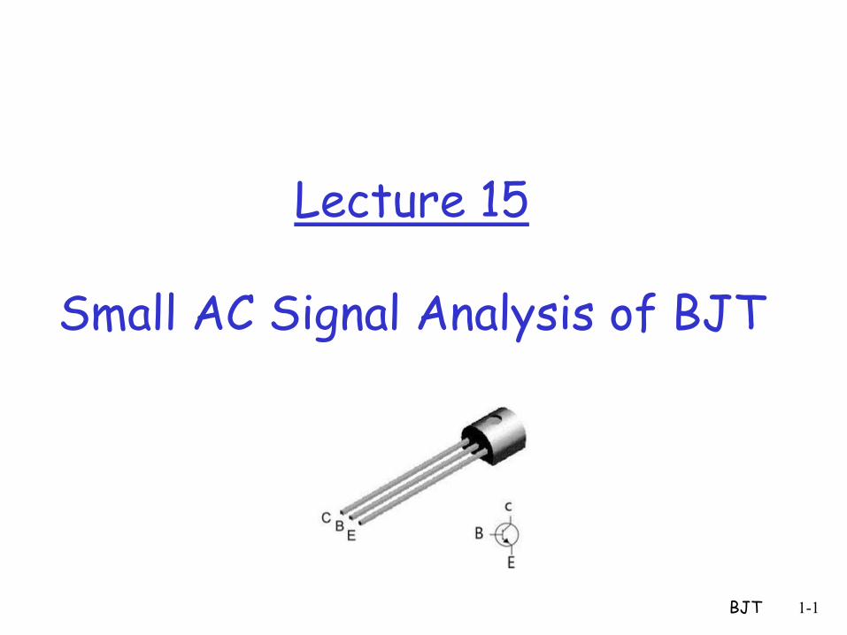
Lecture 15
Small AC Signal Analysis of BJT
BJT 1-1
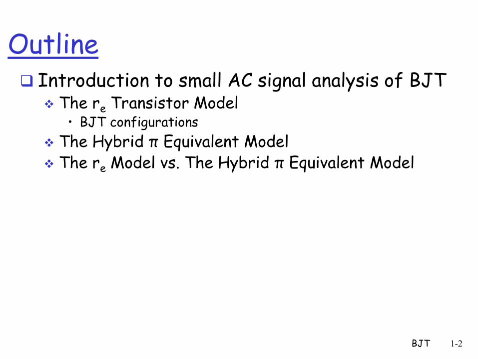
Outline Introduction to small AC signal analysis of BJT
The re Transistor Model • BJT configurations
The Hybrid π Equivalent Model The re Model vs. The Hybrid π Equivalent Model
BJT 1-2
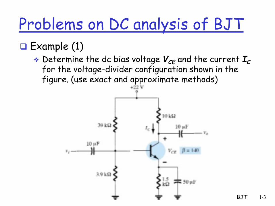
Problems on DC analysis of BJT Example (1)
Determine the dc bias voltage VCE and the current IC for the voltage-divider configuration shown in the figure. (use exact and approximate methods)
BJT 1-3
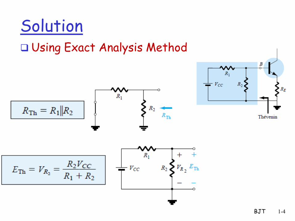
Solution Using Exact Analysis Method
BJT 1-4
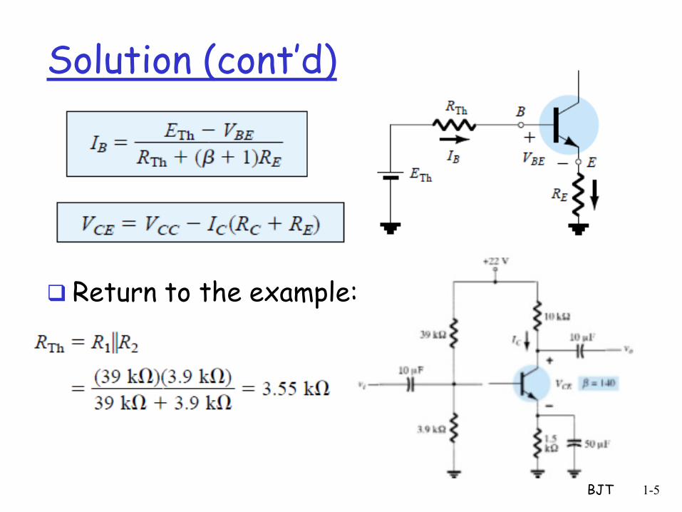
Solution (cont’d)
Return to the example:
BJT 1-5
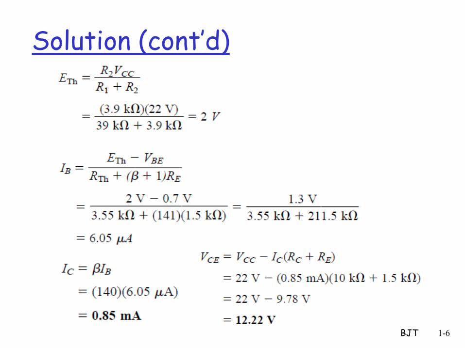
Solution (cont’d)
BJT 1-6
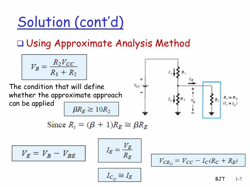
Solution (cont’d)
Using Approximate Analysis Method
BJT 1-7
The condition that will define whether the approximate approach can be applied
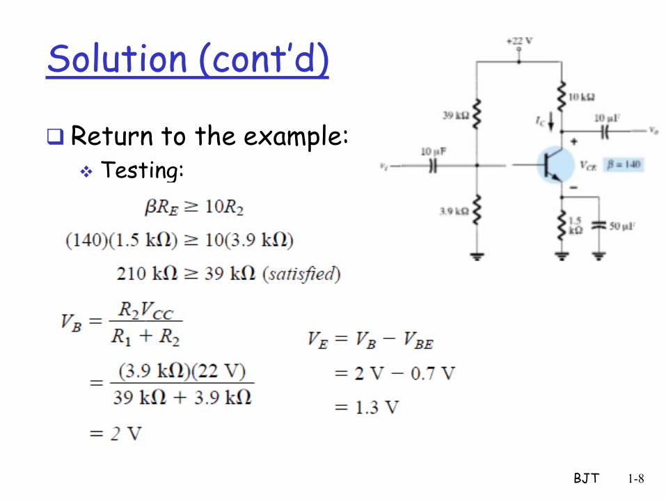
Solution (cont’d)
Return to the example: Testing:
BJT 1-8
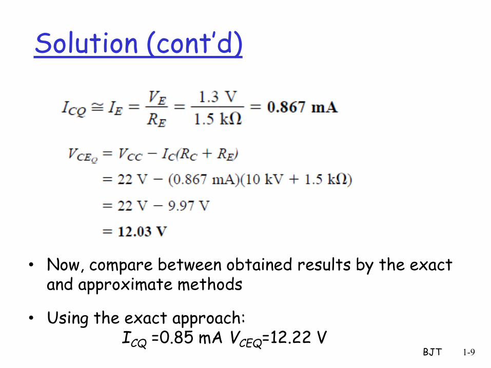
Solution (cont’d)
BJT 1-9
• Now, compare between obtained results by the exact and approximate methods
• Using the exact approach: ICQ =0.85 mA VCEQ=12.22 V
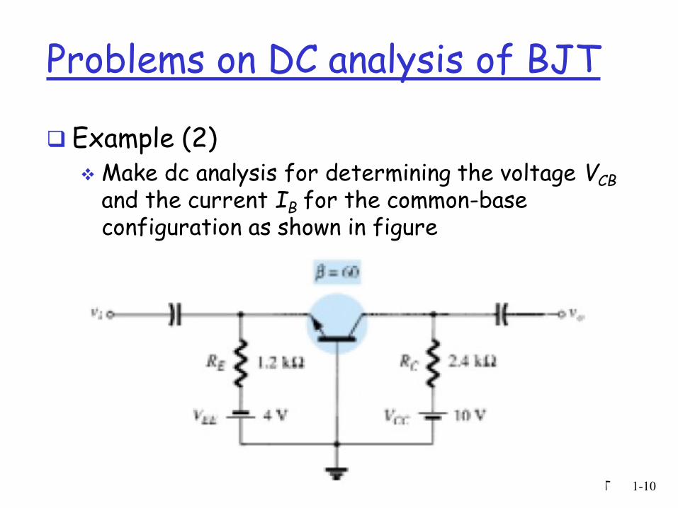
Problems on DC analysis of BJT
Example (2) Make dc analysis for determining the voltage VCB
and the current IB for the common-base configuration as shown in figure
BJT 1-10
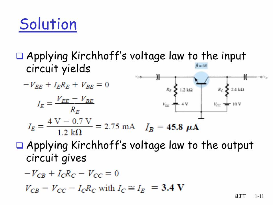
Solution
Applying Kirchhoff’s voltage law to the input circuit yields
Applying Kirchhoff’s voltage law to the output circuit gives
BJT 1-11
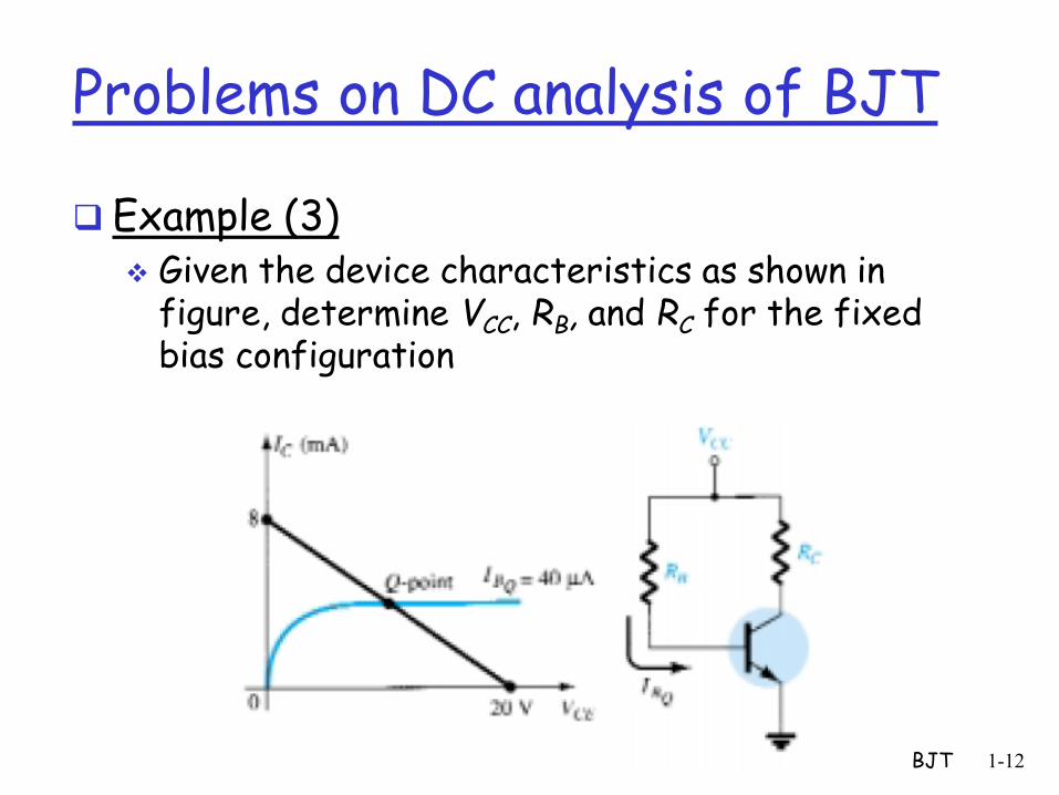
Problems on DC analysis of BJT
Example (3) Given the device characteristics as shown in
figure, determine VCC, RB, and RC for the fixed bias configuration
BJT 1-12
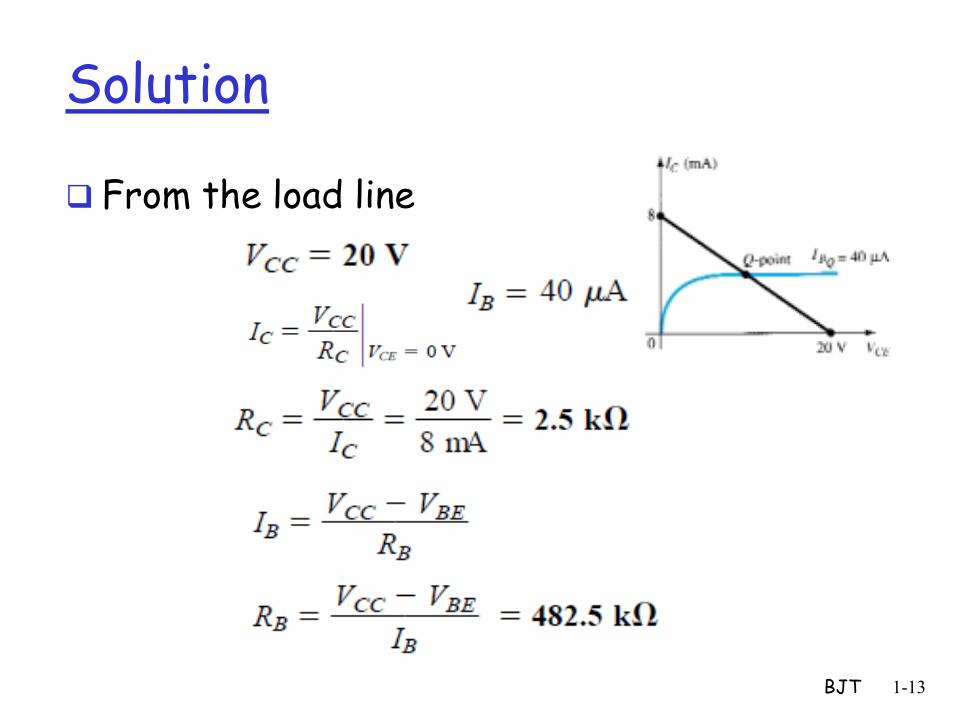
Solution
From the load line
BJT 1-13
BJT Transistor Modeling
BJT AC model is an equivalent circuit that represents the AC characteristics of the BJT transistor
The model uses circuit elements that approximate the behavior of the transistor
There are two models commonly used in small signal AC analysis of a transistor: re model
Hybrid π equivalent model
BJT 1-14
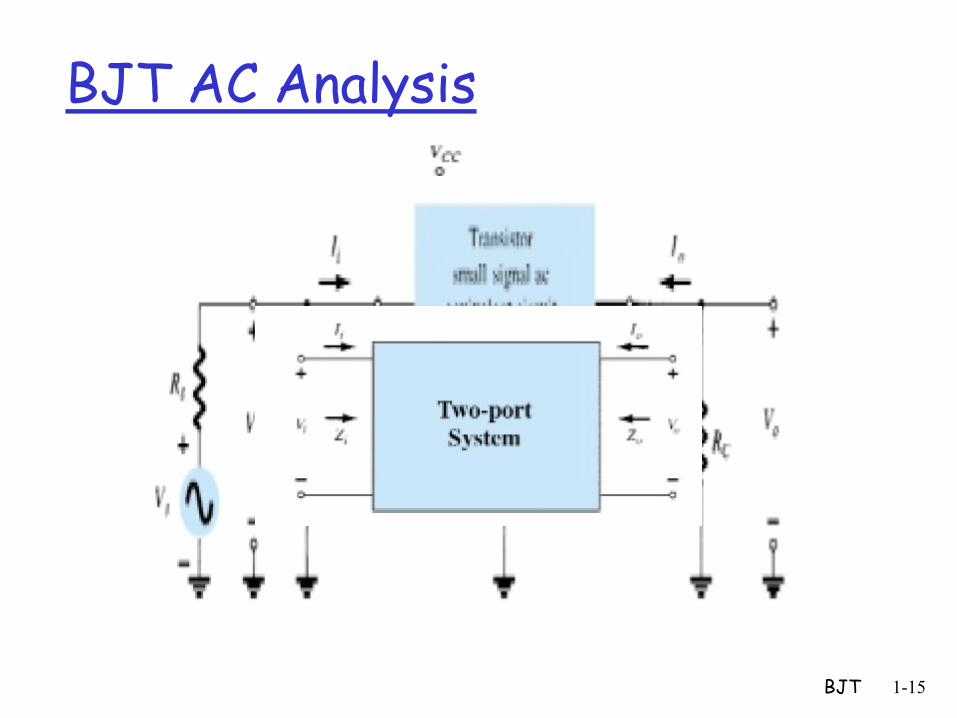
BJT AC Analysis
BJT 1-15
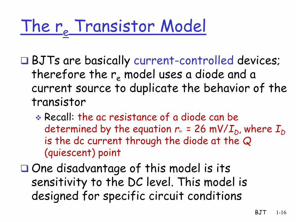
The re Transistor Model
BJTs are basically current-controlled devices; therefore the re model uses a diode and a current source to duplicate the behavior of the transistor Recall: the ac resistance of a diode can be
determined by the equation rac = 26 mV/ID, where ID
is the dc current through the diode at the Q (quiescent) point
One disadvantage of this model is its sensitivity to the DC level. This model is designed for specific circuit conditions
BJT 1-16
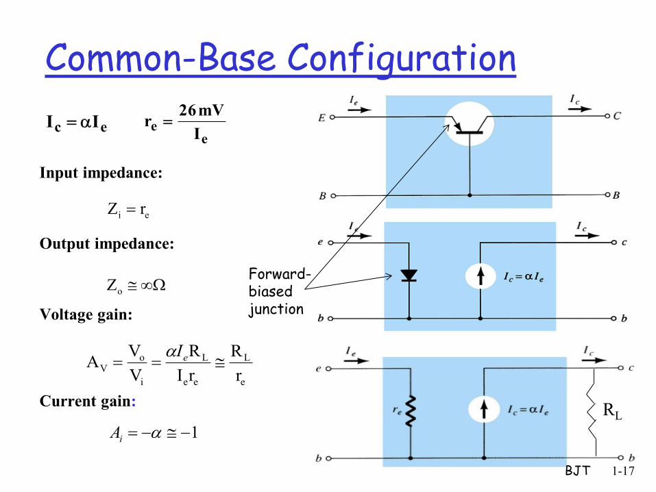
Common-Base Configuration
BJT 1-17
ee
I
mV 26r
Input impedance:
Output impedance:
Voltage gain:
Current gain:
ec I I
ei rZ
oZ
e
L
ee
L
i
oV
r
R
rI
R
V
VA eI
1 iA
RL
Forward-biased junction
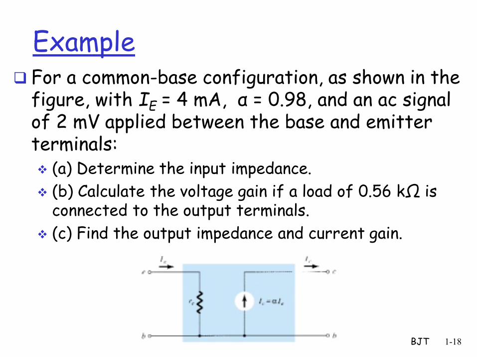
Example For a common-base configuration, as shown in the
figure, with IE = 4 mA, α = 0.98, and an ac signal of 2 mV applied between the base and emitter terminals: (a) Determine the input impedance.
(b) Calculate the voltage gain if a load of 0.56 kΩ is connected to the output terminals.
(c) Find the output impedance and current gain.
BJT 1-18
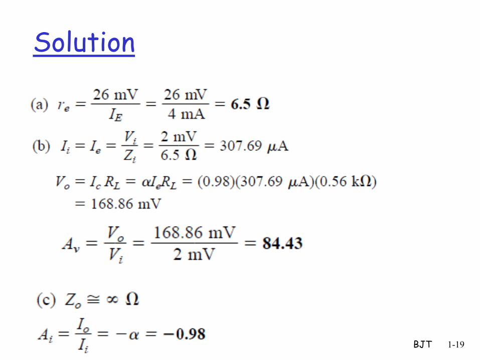
Solution
BJT 1-19
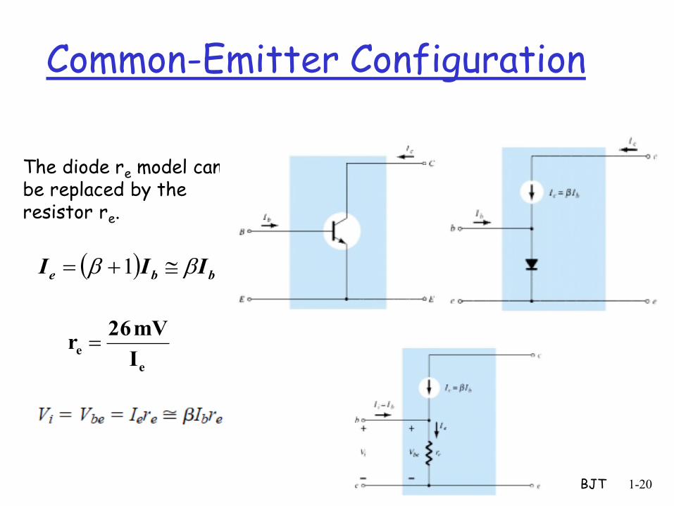
Common-Emitter Configuration
BJT 1-20
bbe III 1
The diode re model can be replaced by the resistor re.
e
eI
mV 26r
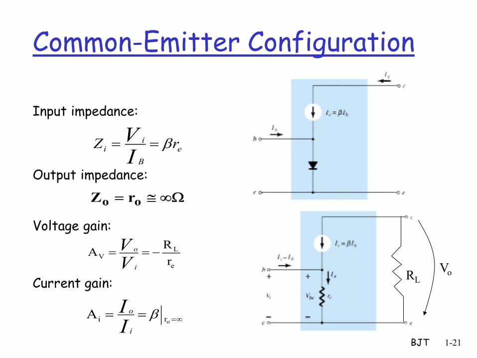
Common-Emitter Configuration
BJT 1-21
Input impedance:
Output impedance:
Voltage gain:
Current gain:
e
B
ii rZIV
oo rZ
e
LV
r
RA VV
i
o
oriA
IIi
o
RL
Vo
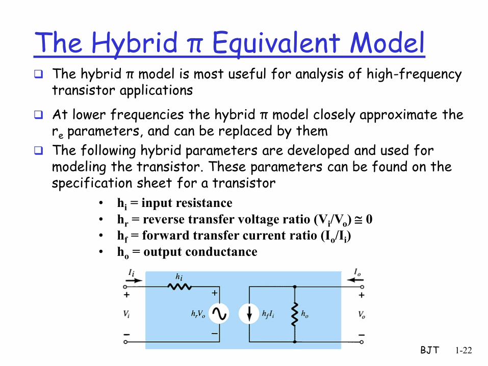
The Hybrid π Equivalent Model The hybrid π model is most useful for analysis of high-frequency
transistor applications
At lower frequencies the hybrid π model closely approximate the re parameters, and can be replaced by them
The following hybrid parameters are developed and used for modeling the transistor. These parameters can be found on the specification sheet for a transistor
BJT 1-22
• hi = input resistance
• hr = reverse transfer voltage ratio (Vi/Vo) 0
• hf = forward transfer current ratio (Io/Ii)
• ho = output conductance
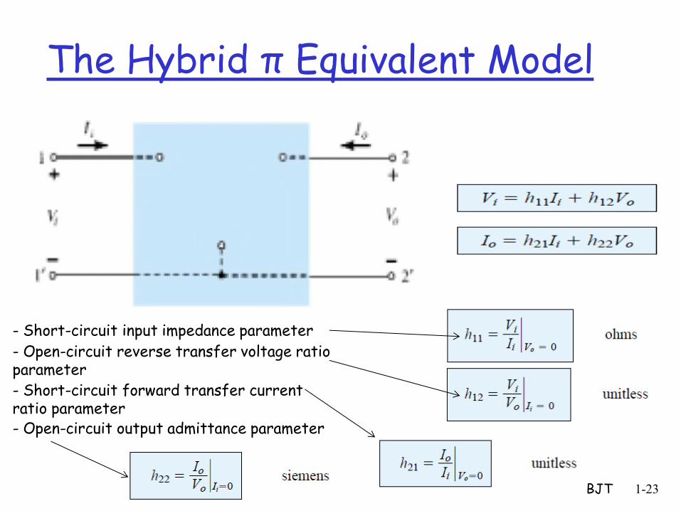
The Hybrid π Equivalent Model
BJT 1-23
- Short-circuit input impedance parameter
- Open-circuit reverse transfer voltage ratio parameter
- Short-circuit forward transfer current ratio parameter - Open-circuit output admittance parameter
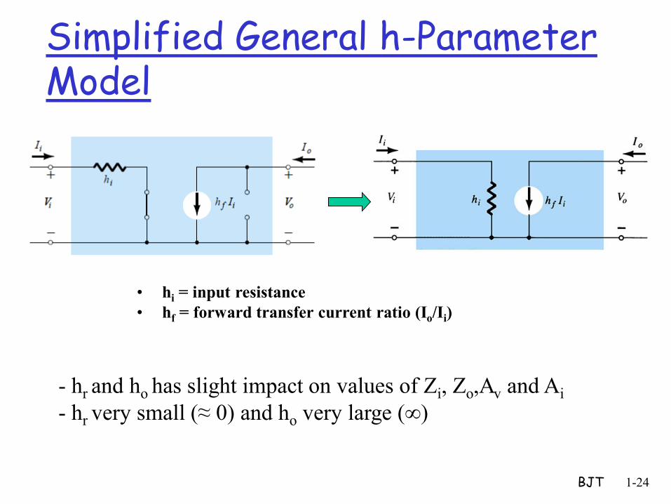
Simplified General h-Parameter Model
BJT 1-24
• hi = input resistance
• hf = forward transfer current ratio (Io/Ii)
- hr and ho has slight impact on values of Zi, Zo,Av and Ai
- hr very small (≈ 0) and ho very large (∞)
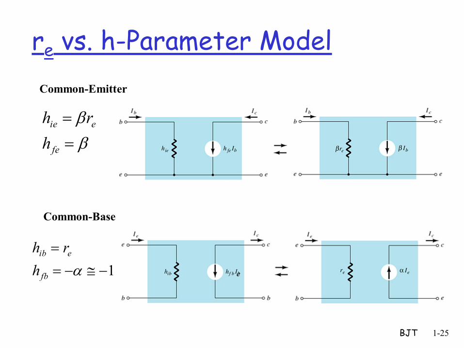
re vs. h-Parameter Model
BJT 1-25
fe
eie
h
rh
Common-Emitter
Common-Base
1
fb
eib
h
rh
e
BJT 1-26
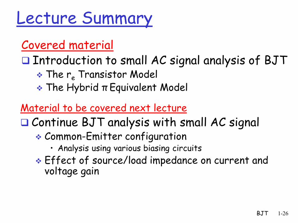
Lecture Summary
Covered material Introduction to small AC signal analysis of BJT
The re Transistor Model The Hybrid π Equivalent Model
Material to be covered next lecture
Continue BJT analysis with small AC signal Common-Emitter configuration
• Analysis using various biasing circuits
Effect of source/load impedance on current and voltage gain


![Lecture 4 BJT Small Signal Analysis01 [??????????????????]pws.npru.ac.th/thawatchait/data/files/Lecture 4 BJT Small... · 2016-09-12 · Lecture 4 BJJg yT Small Signal Analysis Present](https://static.fdocument.org/doc/165x107/5e674360ee8da93175055e37/lecture-4-bjt-small-signal-analysis01-pwsnpruacththawatchaitdatafileslecture.jpg)