L. Hart, James Nathaniel, Mitra L. Taheri, Fan Ren, S. J ...
6
Diffusion of implanted Ge and Sn in β-Ga 2 O 3 Ribhu Sharma, Mark E. Law, Minghan Xian, Marko Tadjer, Elaf A. Anber, Daniel Foley, Andrew C. Lang, James L. Hart, James Nathaniel, Mitra L. Taheri, Fan Ren, S. J. Pearton, and A. Kuramata Citation: Journal of Vacuum Science & Technology B 37, 051204 (2019); doi: 10.1116/1.5118001 View online: https://doi.org/10.1116/1.5118001 View Table of Contents: https://avs.scitation.org/toc/jvb/37/5 Published by the American Vacuum Society
Transcript of L. Hart, James Nathaniel, Mitra L. Taheri, Fan Ren, S. J ...

Diffusion of implanted Ge and Sn in β-Ga2O3Ribhu Sharma, Mark E. Law, Minghan Xian, Marko Tadjer, Elaf A. Anber, Daniel Foley, Andrew C. Lang, JamesL. Hart, James Nathaniel, Mitra L. Taheri, Fan Ren, S. J. Pearton, and A. Kuramata
Citation: Journal of Vacuum Science & Technology B 37, 051204 (2019); doi: 10.1116/1.5118001View online: https://doi.org/10.1116/1.5118001View Table of Contents: https://avs.scitation.org/toc/jvb/37/5Published by the American Vacuum Society
Diffusion of implanted Ge and Sn in β-Ga2O3
Ribhu Sharma,1 Mark E. Law,2 Minghan Xian,3 Marko Tadjer,4 Elaf A. Anber,5
Daniel Foley,5 Andrew C. Lang,5 James L. Hart,5 James Nathaniel,5 Mitra L. Taheri,5
Fan Ren,3 S. J. Pearton,1,a) and A. Kuramata61Department of Materials Science and Engineering, University of Florida, Gainesville, Florida 326112Department of Electrical and Computer Engineering, University of Florida, Gainesville, Florida 326113Department of Chemical Engineering, University of Florida, Gainesville, Florida 326114U.S. Naval Research Laboratory, 4555 Overlook Ave. SW, Washington, DC 203755Department of Materials Science and Engineering, Drexel University, Philadelphia, Pennsylvania 191046Tamura Corp. and Novel Crystal Technology, Sayama City, Saitama 350-1328, Japan
(Received 2 July 2019; accepted 5 August 2019; published 27 August 2019)
The n-type dopants, Ge and Sn, were implanted into bulk (−201) β-Ga2O3 at multiple energies(60, 100, 200 keV) and total doses of ∼1014 cm−2 and annealed at 1100 °C for 10–120 s under eitherO2 or N2 ambients. The Ge-implanted samples showed almost complete recovery of the initialdamage band under these conditions, with the disordered region decreasing from 130 to 17 nm after1100 °C anneals. Fitting of secondary ion mass spectrometry profiles was used to obtain the diffusiv-ity of both Ge and Sn, with values at 1100 °C of 1.05 × 10⁻¹¹ cm s−1 for Ge and 2.7 × 10⁻¹³ cm s−1
for Sn for annealing under O2 ambients. Some of the dopant is lost to the surface during theseanneals, with a surface outgas rate of 1–3 × 10⁻⁷ s−1. By sharp contrast, the redistribution of bothdopants was almost completely suppressed during annealing in N2 ambients under the same condi-tions, showing the strong influence of point defects on dopant diffusivity of these implanted dopantsin β-Ga2O3. Published by the AVS. https://doi.org/10.1116/1.5118001
I. INTRODUCTION
N-type doping of β-Ga2O3 during crystal growth is typi-cally performed with the tetravalent ions Si, Sn, and Ge,which have hydrogenic shallow donor states (ionization levelsin the range of 10–30 meV).1–7 It has been noted that hightemperature annealing of undoped and Sn-doped bulk crystalscan have significant effects on the resulting conductivity, espe-cially in O2 ambients, where the material may becomeinsulating.6,8–11 The initial work on β-Ga2O3 found that unin-tentionally doped samples showed increasing charge carrierconcentrations upon annealing in reducing atmospheres,2,5
suggesting that oxygen vacancies were the dominant donorspresent. However, it is now known that oxygen vacancies aredeep donors and do not contribute significantly to the n-typeconduction,12 which is now attributed to impurities like Si.5
Similarly, the active fraction of Si is <50% in bulk crystals,indicating that not all are occupying substitutional Ga sites,although there are two Ga sites in the Ga2O3 lattice, and it isexpected that the ionization level is lower for the Ga(I) sitecompared to the octahedral Ga(II) site.13,14 Ge and Sn areoften preferred as dopants, especially in molecular beamepitaxy, because of reduced problems with oxidation of thedopant sources relative to Si.15–17 Finally, Ge should be anideal fit for Ga substitution, based on their similar sizes and,therefore, potentially be an efficient donor impurity.
There is increasing interest in doping Ga2O3 using ionimplantation.18–26 This provides a versatile method for dopingselective area channel and contact regions in field effect tran-sistors.18,19 Implantation can also be used to create resistive,current-defining paths by incorporating deep acceptors like Fe,
MgGa, and NO.20−24 Peelaers et al.27 examined the diffusion
mechanisms for Mg and N and found that diffusion of N waspredominantly assisted by O vacancies, while Mg diffusionwas controlled by the gallium interstitial concentration. Tadjeret al.26 reported diffusivities at 1150 °C of 9.5 × 10⁻¹³ cm2 s−1
for implanted Si and 1.7 × 10⁻¹³ cm2 s−1 for Sn whenannealed under O2. Sharma et al.28 noted a strong dependenceof diffusivity of implanted Si on whether N2 or O2 annealingambients were used, emphasizing the role of defects in assist-ing implanted dopant migration. Wong et al.29 also noted thatimplantation damage enhanced the diffusivity of Fe in adjoin-ing layers as a result of defect migration during annealing.There is clearly a need to more fully understand the diffusionof implanted dopants in Ga2O3 if this approach is to be usedin a controlled fashion during device fabrication.
In this paper, unintentionally doped, edge-defined, film-fed(EFG)-grown (−201) β-Ga2O3 substrates were implanted withGe or Sn ions with multiple energies in the 60–200 keV rangein order to obtain a peak concentration of both dopants of∼1019 cm−3. The samples were then annealed at 1100 °C forvarious times (10–120 s) under O2 or N2 ambients to repair theion damage and activate the donors onto substitutional latticesites. The samples were characterized by secondary ion massspectrometry (SIMS) and cross-sectional transmission electronmicroscopy (TEM) before and after annealing. Both dopantswere found to exhibit significant diffusivity for annealingunder O2 ambient, but this was suppressed in N2 ambients.
II. EXPERIMENT
The samples were obtained from Novel CrystalTechnology6 and were unintentionally doped EFG Ga2O3 sub-strates (no epi), with a room temperature carrier concentrationa)Electronic mail: [email protected]
051204-1 J. Vac. Sci. Technol. B 37(5), Sep/Oct 2019 2166-2746/2019/37(5)/051204/5/$30.00 Published by the AVS. 051204-1
of 1–2 × 1017 cm−3, as measured by the electrochemicalcapacitance-voltage method. They had (−201) orientation,with XRD FWHM rocking curves of 20 arcsec and 25 arcsecin the [010] and [102] directions, respectively.
All samples were implanted nominally at room temperaturewith a 7° tilt with respect to the beam normal. Ge and Sn ionsat multiple energies and doses were employed to obtain near-uniform concentrations of 1019 cm−3. The specific energy anddose conditions were 2 × 1013 cm−2/60 keV + 3 × 1013 cm−2/100 keV + 4 × 1013 cm−2/200 keV for Sn and 3 × 1013 cm−2/60 keV+ 5× 1013cm−2/100 keV+ 7 × 1013cm−2/200 keV for Ge.
The samples were annealed in 1 atm of pure, flowing N2
or O2 at 1100 °C for various times (10–120 s) in a SurfaceScience Integration (SSI) Solaris 150 rapid thermal annealsystem. Microstructural analysis was carried out onGe-implanted and annealed samples using Scanning TEM(STEM) mode on a JEOL 2100 field emission TEM,equipped with a high-resolution pole piece. SIMS was per-formed at Evans Analytical with a magnetic sector Camecasystem using a Cs+ ion beam with 14.5 keV energy and 24°incident angle. The SIMS profiles were fitted using theFLorida Object Oriented Device Process Simulator(FLOOPS) via a Fick diffusion-based model.30,31
III. RESULTS AND DISCUSSION
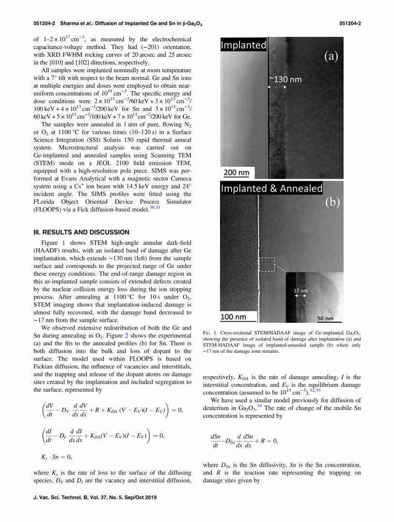
Figure 1 shows STEM high-angle annular dark-field(HAADF) results, with an isolated band of damage after Geimplantation, which extends ∼130 nm (left) from the samplesurface and corresponds to the projected range of Ge underthese energy conditions. The end-of-range damage region inthis as-implanted sample consists of extended defects createdby the nuclear collision energy loss during the ion stoppingprocess. After annealing at 1100 °C for 10 s under O2,STEM imaging shows that implantation-induced damage isalmost fully recovered, with the damage band decreased to∼17 nm from the sample surface.
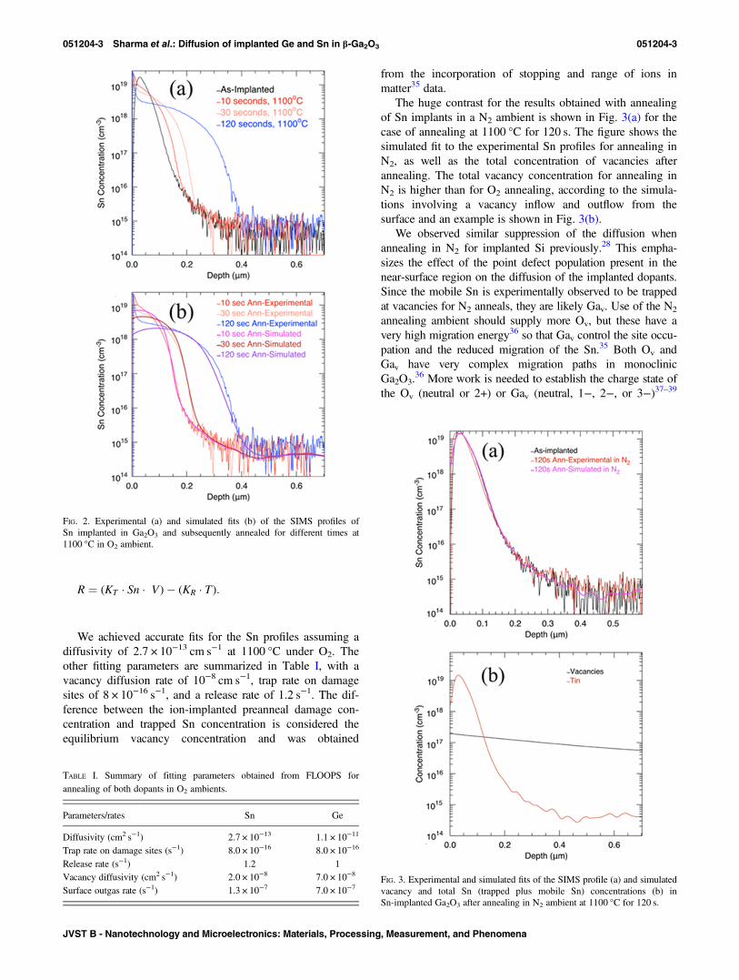
We observed extensive redistribution of both the Ge andSn during annealing in O2. Figure 2 shows the experimental(a) and the fits to the annealed profiles (b) for Sn. There isboth diffusion into the bulk and loss of dopant to thesurface. The model used within FLOOPS is based onFickian diffusion, the influence of vacancies and interstitials,and the trapping and release of the dopant atoms on damagesites created by the implantation and included segregation tothe surface, represented by
dV
dt� DV
d
dx
dV
dxþ Rþ KDA (V � EV )(I � EV )
� �¼ 0,
dI
dt� DI
d
dx
dI
dxþ KDA(V � EV )(I � EV )
� �¼ 0,
Ks � Sn ¼ 0,
where Ks is the rate of loss to the surface of the diffusingspecies, DV and DI are the vacancy and interstitial diffusion,
respectively, KDA is the rate of damage annealing, I is theinterstitial concentration, and EV is the equilibrium damageconcentration (assumed to be 1015 cm−3).32,33
We have used a similar model previously for diffusion ofdeuterium in Ga2O3.
34 The rate of change of the mobile Snconcentration is represented by
dSn
dt–DSn
d
dx
dSn
dxþ R ¼ 0,
where DSn is the Sn diffusivity, Sn is the Sn concentration,and R is the reaction rate representing the trapping ondamage sites given by
FIG. 1. Cross-sectional STEM/HADAAF image of Ge-implanted Ga2O3,showing the presence of isolated band of damage after implantation (a) andSTEM-HADAAF image of implanted-annealed sample (b) where only∼17 nm of the damage zone remains.
051204-2 Sharma et al.: Diffusion of implanted Ge and Sn in β-Ga2O3 051204-2
J. Vac. Sci. Technol. B, Vol. 37, No. 5, Sep/Oct 2019
R ¼ (KT � Sn � V)� (KR � T):
We achieved accurate fits for the Sn profiles assuming adiffusivity of 2.7 × 10⁻¹³ cm s−1 at 1100 °C under O2. Theother fitting parameters are summarized in Table I, with avacancy diffusion rate of 10−8 cm s−1, trap rate on damagesites of 8 × 10⁻¹⁶ s−1, and a release rate of 1.2 s−1. The dif-ference between the ion-implanted preanneal damage con-centration and trapped Sn concentration is considered theequilibrium vacancy concentration and was obtained
from the incorporation of stopping and range of ions inmatter35 data.
The huge contrast for the results obtained with annealingof Sn implants in a N2 ambient is shown in Fig. 3(a) for thecase of annealing at 1100 °C for 120 s. The figure shows thesimulated fit to the experimental Sn profiles for annealing inN2, as well as the total concentration of vacancies afterannealing. The total vacancy concentration for annealing inN2 is higher than for O2 annealing, according to the simula-tions involving a vacancy inflow and outflow from thesurface and an example is shown in Fig. 3(b).
We observed similar suppression of the diffusion whenannealing in N2 for implanted Si previously.28 This empha-sizes the effect of the point defect population present in thenear-surface region on the diffusion of the implanted dopants.Since the mobile Sn is experimentally observed to be trappedat vacancies for N2 anneals, they are likely Gav. Use of the N2
annealing ambient should supply more Ov, but these have avery high migration energy36 so that Gav control the site occu-pation and the reduced migration of the Sn.35 Both Ov andGav have very complex migration paths in monoclinicGa2O3.
36 More work is needed to establish the charge state ofthe Ov (neutral or 2+) or Gav (neutral, 1−, 2−, or 3−)37–39
TABLE I. Summary of fitting parameters obtained from FLOOPS forannealing of both dopants in O2 ambients.
Parameters/rates Sn Ge
Diffusivity (cm2 s−1) 2.7 × 10⁻¹³ 1.1 × 10⁻¹¹
Trap rate on damage sites (s−1) 8.0 × 10⁻¹⁶ 8.0 × 10⁻¹⁶
Release rate (s−1) 1.2 1Vacancy diffusivity (cm2 s−1) 2.0 × 10⁻⁸ 7.0 × 10⁻⁸
Surface outgas rate (s−1) 1.3 × 10⁻⁷ 7.0 × 10⁻⁷FIG. 3. Experimental and simulated fits of the SIMS profile (a) and simulatedvacancy and total Sn (trapped plus mobile Sn) concentrations (b) inSn-implanted Ga2O3 after annealing in N2 ambient at 1100 °C for 120 s.
FIG. 2. Experimental (a) and simulated fits (b) of the SIMS profiles ofSn implanted in Ga2O3 and subsequently annealed for different times at1100 °C in O2 ambient.
051204-3 Sharma et al.: Diffusion of implanted Ge and Sn in β-Ga2O3 051204-3
JVST B - Nanotechnology and Microelectronics: Materials, Processing, Measurement, and Phenomena
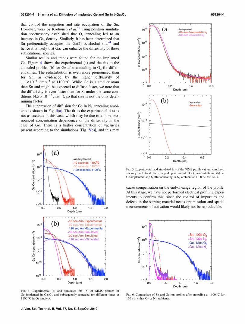
that control the migration and site occupation of the Sn.However, work by Korhonen et al.40 using positron annihila-tion spectroscopy established that O2 annealing led to anincrease in Gav density. Similarly, it has been determined thatSn preferentially occupies the Ga(2) octahedral site,41 andhence it is likely that Gav can enhance the diffusivity of thesesubstitutional species.
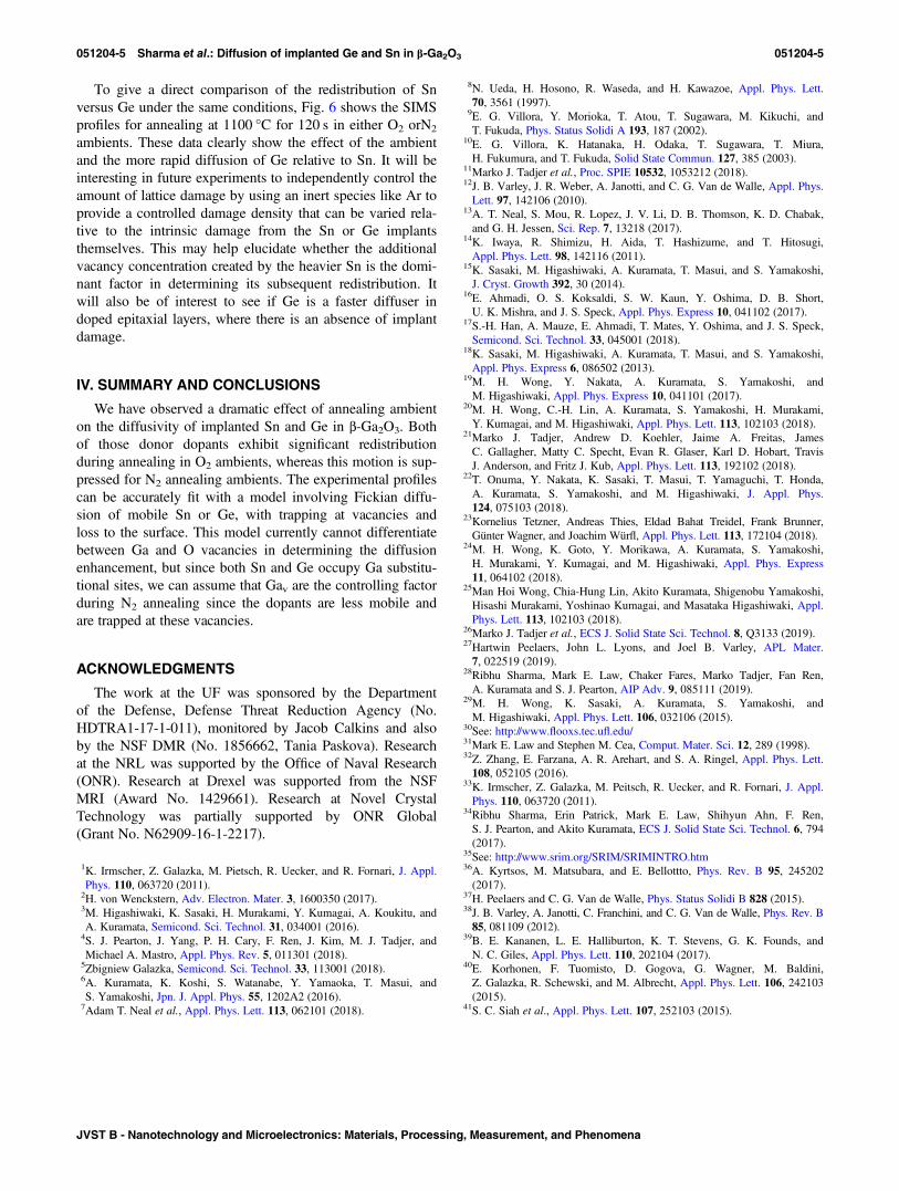
Similar results and trends were found for the implantedGe. Figure 4 shows the experimental (a) and the fits to theannealed profiles (b) for Ge after annealing in O2 for differ-ent times. The redistribution is even more pronounced thanfor Sn, as evidenced by the higher diffusivity of1.1 × 10−11 cm s−1 at 1100 °C. While Ge is a smaller atomthan Sn and might be expected to diffuse faster, we note thatthe diffusivity is even faster than for Si under the same con-ditions (4.5 × 10⁻¹² cms−1), so that size is not the only deter-mining factor.
The suppression of diffusion for Ge in N2 annealing ambi-ents is shown in Fig. 5(a). The fit to the experimental data isnot as accurate in this case, which may be due to a more pro-nounced concentration dependence of the diffusivity in thecase of Ge. There is a higher concentration of vacanciespresent according to the simulations [Fig. 5(b)], and this may
cause compensation on the end-of-range region of the profile.At this stage, we have not performed electrical profiling exper-iments to confirm this, since the control of impurities anddefects in the starting material needs optimization and spatialmeasurements of activation would likely not be reproducible.
FIG. 4. Experimental (a) and simulated fits (b) of SIMS profiles ofGe implanted in Ga2O3 and subsequently annealed for different times at1100 °C in O2 ambient.
FIG. 5. Experimental and simulated fits of the SIMS profile (a) and simulatedvacancy and total Ge (trapped plus mobile Ge) concentrations (b) inGe-implanted Ga2O3 after annealing in N2 ambient at 1100 °C for 120 s.
FIG. 6. Comparison of Sn and Ge ion profiles after annealing at 1100 °C for120 s in either O2 or N2 ambients.
051204-4 Sharma et al.: Diffusion of implanted Ge and Sn in β-Ga2O3 051204-4
J. Vac. Sci. Technol. B, Vol. 37, No. 5, Sep/Oct 2019
To give a direct comparison of the redistribution of Snversus Ge under the same conditions, Fig. 6 shows the SIMSprofiles for annealing at 1100 °C for 120 s in either O2 orN2
ambients. These data clearly show the effect of the ambientand the more rapid diffusion of Ge relative to Sn. It will beinteresting in future experiments to independently control theamount of lattice damage by using an inert species like Ar toprovide a controlled damage density that can be varied rela-tive to the intrinsic damage from the Sn or Ge implantsthemselves. This may help elucidate whether the additionalvacancy concentration created by the heavier Sn is the domi-nant factor in determining its subsequent redistribution. Itwill also be of interest to see if Ge is a faster diffuser indoped epitaxial layers, where there is an absence of implantdamage.
IV. SUMMARY AND CONCLUSIONS
We have observed a dramatic effect of annealing ambienton the diffusivity of implanted Sn and Ge in β-Ga2O3. Bothof those donor dopants exhibit significant redistributionduring annealing in O2 ambients, whereas this motion is sup-pressed for N2 annealing ambients. The experimental profilescan be accurately fit with a model involving Fickian diffu-sion of mobile Sn or Ge, with trapping at vacancies andloss to the surface. This model currently cannot differentiatebetween Ga and O vacancies in determining the diffusionenhancement, but since both Sn and Ge occupy Ga substitu-tional sites, we can assume that Gav are the controlling factorduring N2 annealing since the dopants are less mobile andare trapped at these vacancies.
ACKNOWLEDGMENTS
The work at the UF was sponsored by the Departmentof the Defense, Defense Threat Reduction Agency (No.HDTRA1-17-1-011), monitored by Jacob Calkins and alsoby the NSF DMR (No. 1856662, Tania Paskova). Researchat the NRL was supported by the Office of Naval Research(ONR). Research at Drexel was supported from the NSFMRI (Award No. 1429661). Research at Novel CrystalTechnology was partially supported by ONR Global(Grant No. N62909-16-1-2217).
1K. Irmscher, Z. Galazka, M. Pietsch, R. Uecker, and R. Fornari, J. Appl.Phys. 110, 063720 (2011).
2H. von Wenckstern, Adv. Electron. Mater. 3, 1600350 (2017).3M. Higashiwaki, K. Sasaki, H. Murakami, Y. Kumagai, A. Koukitu, andA. Kuramata, Semicond. Sci. Technol. 31, 034001 (2016).
4S. J. Pearton, J. Yang, P. H. Cary, F. Ren, J. Kim, M. J. Tadjer, andMichael A. Mastro, Appl. Phys. Rev. 5, 011301 (2018).
5Zbigniew Galazka, Semicond. Sci. Technol. 33, 113001 (2018).6A. Kuramata, K. Koshi, S. Watanabe, Y. Yamaoka, T. Masui, andS. Yamakoshi, Jpn. J. Appl. Phys. 55, 1202A2 (2016).
7Adam T. Neal et al., Appl. Phys. Lett. 113, 062101 (2018).
8N. Ueda, H. Hosono, R. Waseda, and H. Kawazoe, Appl. Phys. Lett.70, 3561 (1997).
9E. G. Villora, Y. Morioka, T. Atou, T. Sugawara, M. Kikuchi, andT. Fukuda, Phys. Status Solidi A 193, 187 (2002).
10E. G. Villora, K. Hatanaka, H. Odaka, T. Sugawara, T. Miura,H. Fukumura, and T. Fukuda, Solid State Commun. 127, 385 (2003).
11Marko J. Tadjer et al., Proc. SPIE 10532, 1053212 (2018).12J. B. Varley, J. R. Weber, A. Janotti, and C. G. Van de Walle, Appl. Phys.Lett. 97, 142106 (2010).
13A. T. Neal, S. Mou, R. Lopez, J. V. Li, D. B. Thomson, K. D. Chabak,and G. H. Jessen, Sci. Rep. 7, 13218 (2017).
14K. Iwaya, R. Shimizu, H. Aida, T. Hashizume, and T. Hitosugi,Appl. Phys. Lett. 98, 142116 (2011).
15K. Sasaki, M. Higashiwaki, A. Kuramata, T. Masui, and S. Yamakoshi,J. Cryst. Growth 392, 30 (2014).
16E. Ahmadi, O. S. Koksaldi, S. W. Kaun, Y. Oshima, D. B. Short,U. K. Mishra, and J. S. Speck, Appl. Phys. Express 10, 041102 (2017).
17S.-H. Han, A. Mauze, E. Ahmadi, T. Mates, Y. Oshima, and J. S. Speck,Semicond. Sci. Technol. 33, 045001 (2018).
18K. Sasaki, M. Higashiwaki, A. Kuramata, T. Masui, and S. Yamakoshi,Appl. Phys. Express 6, 086502 (2013).
19M. H. Wong, Y. Nakata, A. Kuramata, S. Yamakoshi, andM. Higashiwaki, Appl. Phys. Express 10, 041101 (2017).
20M. H. Wong, C.-H. Lin, A. Kuramata, S. Yamakoshi, H. Murakami,Y. Kumagai, and M. Higashiwaki, Appl. Phys. Lett. 113, 102103 (2018).
21Marko J. Tadjer, Andrew D. Koehler, Jaime A. Freitas, JamesC. Gallagher, Matty C. Specht, Evan R. Glaser, Karl D. Hobart, TravisJ. Anderson, and Fritz J. Kub, Appl. Phys. Lett. 113, 192102 (2018).
22T. Onuma, Y. Nakata, K. Sasaki, T. Masui, T. Yamaguchi, T. Honda,A. Kuramata, S. Yamakoshi, and M. Higashiwaki, J. Appl. Phys.124, 075103 (2018).
23Kornelius Tetzner, Andreas Thies, Eldad Bahat Treidel, Frank Brunner,Günter Wagner, and Joachim Würfl, Appl. Phys. Lett. 113, 172104 (2018).
24M. H. Wong, K. Goto, Y. Morikawa, A. Kuramata, S. Yamakoshi,H. Murakami, Y. Kumagai, and M. Higashiwaki, Appl. Phys. Express11, 064102 (2018).
25Man Hoi Wong, Chia-Hung Lin, Akito Kuramata, Shigenobu Yamakoshi,Hisashi Murakami, Yoshinao Kumagai, and Masataka Higashiwaki, Appl.Phys. Lett. 113, 102103 (2018).
26Marko J. Tadjer et al., ECS J. Solid State Sci. Technol. 8, Q3133 (2019).27Hartwin Peelaers, John L. Lyons, and Joel B. Varley, APL Mater.7, 022519 (2019).
28Ribhu Sharma, Mark E. Law, Chaker Fares, Marko Tadjer, Fan Ren,A. Kuramata and S. J. Pearton, AIP Adv. 9, 085111 (2019).
29M. H. Wong, K. Sasaki, A. Kuramata, S. Yamakoshi, andM. Higashiwaki, Appl. Phys. Lett. 106, 032106 (2015).
30See: http://www.flooxs.tec.ufl.edu/31Mark E. Law and Stephen M. Cea, Comput. Mater. Sci. 12, 289 (1998).32Z. Zhang, E. Farzana, A. R. Arehart, and S. A. Ringel, Appl. Phys. Lett.108, 052105 (2016).
33K. Irmscher, Z. Galazka, M. Peitsch, R. Uecker, and R. Fornari, J. Appl.Phys. 110, 063720 (2011).
34Ribhu Sharma, Erin Patrick, Mark E. Law, Shihyun Ahn, F. Ren,S. J. Pearton, and Akito Kuramata, ECS J. Solid State Sci. Technol. 6, 794(2017).
35See: http://www.srim.org/SRIM/SRIMINTRO.htm36A. Kyrtsos, M. Matsubara, and E. Bellottto, Phys. Rev. B 95, 245202(2017).
37H. Peelaers and C. G. Van de Walle, Phys. Status Solidi B 828 (2015).38J. B. Varley, A. Janotti, C. Franchini, and C. G. Van de Walle, Phys. Rev. B85, 081109 (2012).
39B. E. Kananen, L. E. Halliburton, K. T. Stevens, G. K. Founds, andN. C. Giles, Appl. Phys. Lett. 110, 202104 (2017).
40E. Korhonen, F. Tuomisto, D. Gogova, G. Wagner, M. Baldini,Z. Galazka, R. Schewski, and M. Albrecht, Appl. Phys. Lett. 106, 242103(2015).
41S. C. Siah et al., Appl. Phys. Lett. 107, 252103 (2015).
051204-5 Sharma et al.: Diffusion of implanted Ge and Sn in β-Ga2O3 051204-5
JVST B - Nanotechnology and Microelectronics: Materials, Processing, Measurement, and Phenomena