KRN-SF-SM-080-10GD 10G SFP+ ZR 1310nm 80KM SMF …€¦ · 10G SFP+ ZR 1310nm 80KM SMF LC DDM...
9
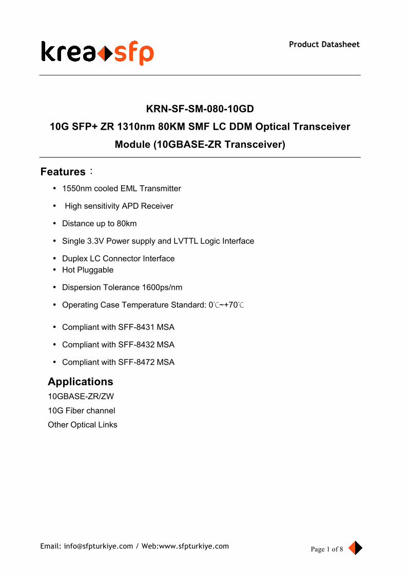
Page 1 of 8 Product Datasheet Email: [email protected] / Web:www.sfpturkiye.com KRN-SF-SM-080-10GD 10G SFP+ ZR 1310nm 80KM SMF LC DDM Optical Transceiver Module (10GBASE-ZR Transceiver) Features: • 1550nm cooled EML Transmitter • High sensitivity APD Receiver • Distance up to 80km • Single 3.3V Power supply and LVTTL Logic Interface • Duplex LC Connector Interface • Hot Pluggable • Dispersion Tolerance 1600ps/nm • Operating Case Temperature Standard: 0℃~+70℃ • Compliant with SFF-8431 MSA • Compliant with SFF-8432 MSA • Compliant with SFF-8472 MSA Applications 10GBASE-ZR/ZW 10G Fiber channel Other Optical Links
-
Upload
truongkhue -
Category
Documents
-
view
218 -
download
1
Transcript of KRN-SF-SM-080-10GD 10G SFP+ ZR 1310nm 80KM SMF …€¦ · 10G SFP+ ZR 1310nm 80KM SMF LC DDM...
Page 1 of 8
Product Datasheet
Email: [email protected] / Web:www.sfpturkiye.com
KRN-SF-SM-080-10GD 10G SFP+ ZR 1310nm 80KM SMF LC DDM Optical Transceiver
Module (10GBASE-ZR Transceiver)
Features:
• 1550nm cooled EML Transmitter
• High sensitivity APD Receiver
• Distance up to 80km
• Single 3.3V Power supply and LVTTL Logic Interface
• Duplex LC Connector Interface • Hot Pluggable
• Dispersion Tolerance 1600ps/nm
• Operating Case Temperature Standard: 0℃~+70℃
• Compliant with SFF-8431 MSA
• Compliant with SFF-8432 MSA
• Compliant with SFF-8472 MSA
Applications
10GBASE-ZR/ZW
10G Fiber channel
Other Optical Links
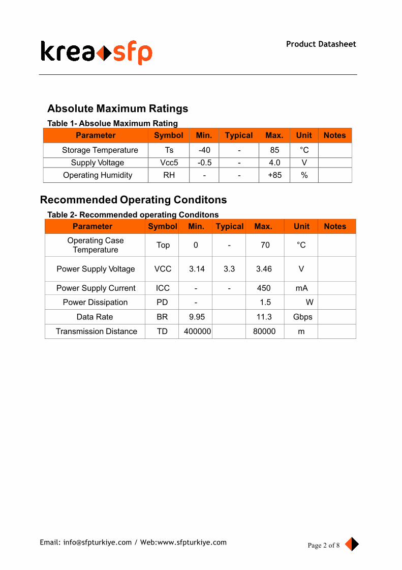
Page 2 of 8
Product Datasheet
Email: [email protected] / Web:www.sfpturkiye.com
Absolute Maximum Ratings
Table 1- Absolue Maximum Rating Parameter Symbol Min. Typical Max. Unit Notes
Storage Temperature Ts -40 - 85 °C
Supply Voltage Vcc5 -0.5 - 4.0 V
Operating Humidity RH - - +85 %
Recommended Operating Conditons
Table 2- Recommended operating Conditons Parameter Symbol Min. Typical Max. Unit Notes
Operating Case Temperature
Top
0
-
70
°C
Power Supply Voltage
VCC
3.14
3.3
3.46
V
Power Supply Current ICC - - 450 mA
Power Dissipation PD - 1.5 W
Data Rate BR 9.95 11.3 Gbps
Transmission Distance TD 400000 80000 m
Page 3 of 8
Product Datasheet
Email: [email protected] / Web:www.sfpturkiye.com
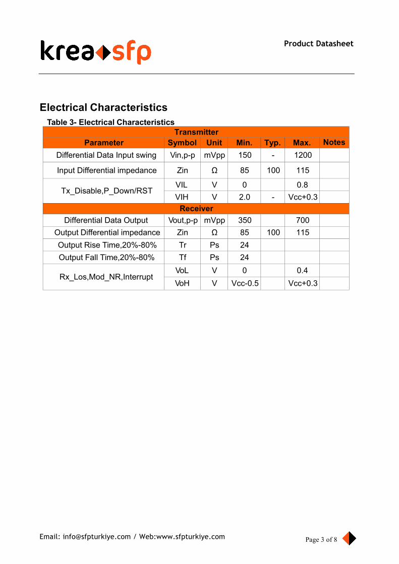
Electrical Characteristics
Table 3- Electrical Characteristics Transmitter
Parameter Symbol Unit Min. Typ. Max. Notes Differential Data Input swing Vin,p-p mVpp 150 - 1200
Input Differential impedance Zin Ω 85 100 115
Tx_Disable,P_Down/RST
VIL V 0 0.8
VIH V 2.0 - Vcc+0.3 Receiver
Differential Data Output Vout,p-p mVpp 350 700
Output Differential impedance Zin Ω 85 100 115
Output Rise Time,20%-80% Tr Ps 24
Output Fall Time,20%-80% Tf Ps 24
Rx_Los,Mod_NR,Interrupt
VoL V 0 0.4
VoH V Vcc-0.5 Vcc+0.3
Page 4 of 8
Product Datasheet
Email: [email protected] / Web:www.sfpturkiye.com
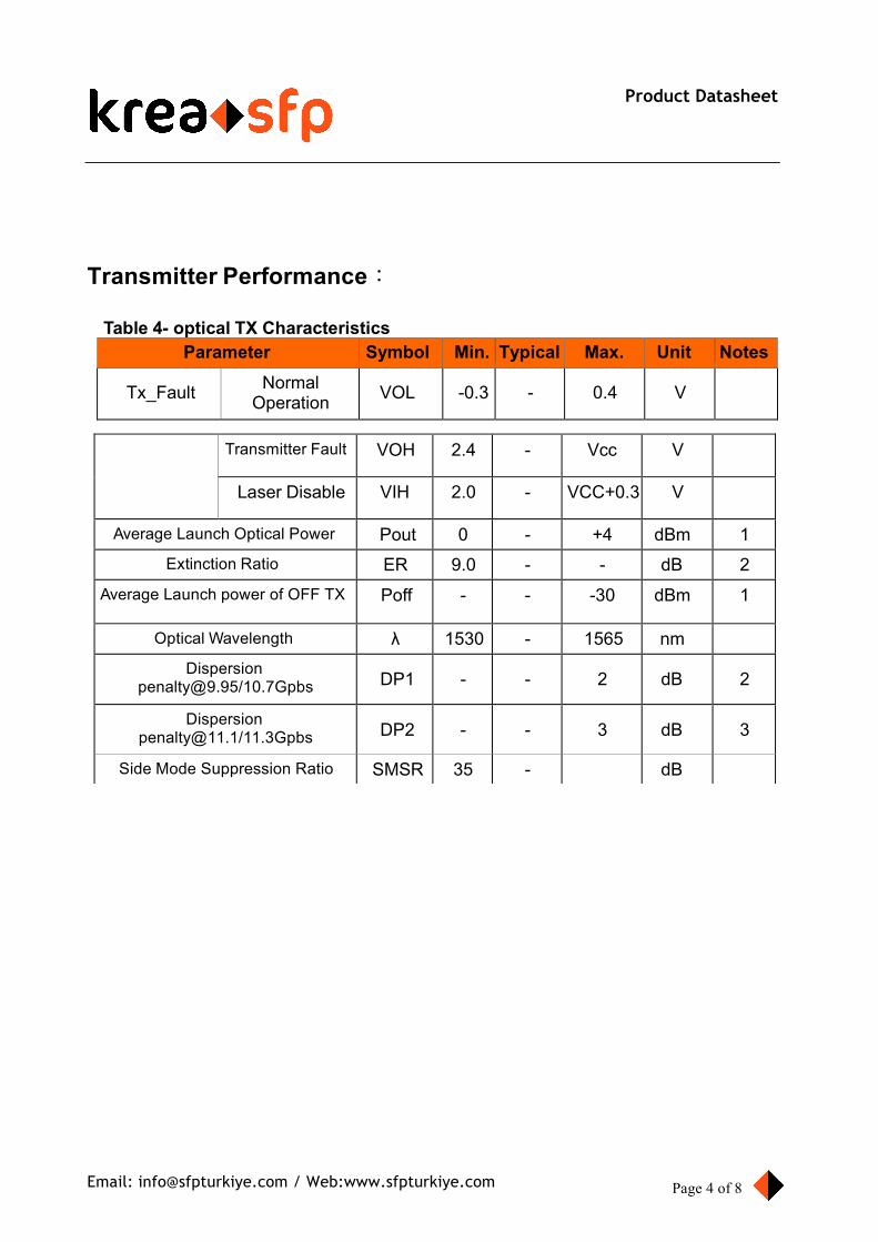
Transmitter Performance:
Table 4- optical TX Characteristics Parameter Symbol Min. Typical Max. Unit Notes
Tx_Fault Normal
Operation
VOL
-0.3
-
0.4
V
Transmitter Fault VOH 2.4 - Vcc V
Laser Disable VIH 2.0 - VCC+0.3 V
Average Launch Optical Power Pout 0 - +4 dBm 1 Extinction Ratio ER 9.0 - - dB 2
Average Launch power of OFF TX Poff - - -30 dBm 1
Optical Wavelength λ 1530 - 1565 nm
Dispersion [email protected]/10.7Gpbs
DP1
-
-
2
dB
2
Dispersion [email protected]/11.3Gpbs
DP2
-
-
3
dB
3
Side Mode Suppression Ratio SMSR 35 - dB
Page 5 of 8
Product Datasheet
Email: [email protected] / Web:www.sfpturkiye.com
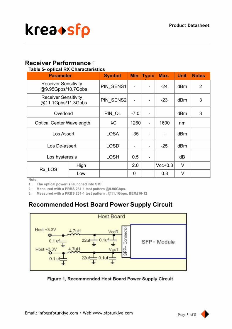
Receiver Performance: Table 5- optical RX Characteristics
Parameter Symbol Min. Typical
Max. Unit Notes
Receiver Sensitivity @9.95Gpbs/10.7Gpbs
PIN_SENS1
-
-
-24
dBm
2
Receiver Sensitivity @11.1Gpbs/11.3Gpbs
PIN_SENS2
-
-
-23
dBm
3
Overload
PIN_OL
-7.0
-
dBm
3
Optical Center Wavelength
λC
1260
-
1600
nm
Los Assert
LOSA
-35
-
-
dBm
Los De-assert
LOSD
-
-
-25
dBm
Los hysteresis
LOSH
0.5
-
dB
Rx_LOS
High 2.0 Vcc+0.3 V
Low 0 0.8 V
Note: 1. The optical power is launched into SMF. 2. Measured with a PRBS 231-1 test pattern @9.95Gbps. 3. Measured with a PRBS 231-1 test pattern , @11.1Gbps. BER≤10-12
Recommended Host Board Power Supply Circuit
Page 6 of 8
Product Datasheet
Email: [email protected] / Web:www.sfpturkiye.com
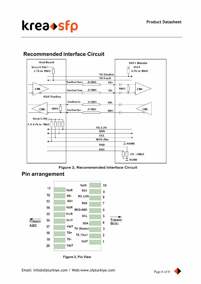
Recommended interface Circuit
Pin arrangement
Page 7 of 8
Product Datasheet
Email: [email protected] / Web:www.sfpturkiye.com
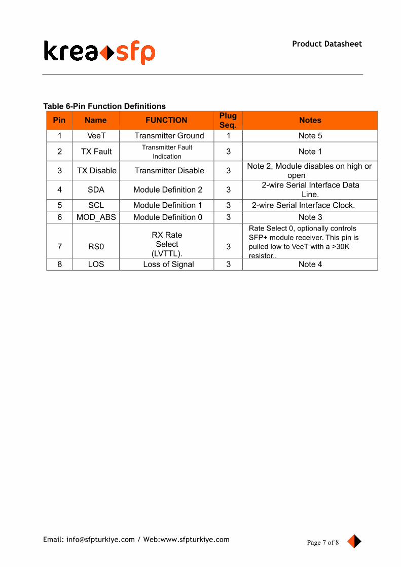
Table 6-Pin Function Definitions
Pin
Name
FUNCTION Plug Seq.
Notes
1 VeeT Transmitter Ground 1 Note 5
2
TX Fault Transmitter Fault Indication
3
Note 1
3
TX Disable
Transmitter Disable
3 Note 2, Module disables on high or open
4
SDA
Module Definition 2
3 2-wire Serial Interface Data Line.
5 SCL Module Definition 1 3 2-wire Serial Interface Clock. 6 MOD_ABS Module Definition 0 3 Note 3
7
RS0
RX Rate Select
(LVTTL).
3
Rate Select 0, optionally controls SFP+ module receiver. This pin is pulled low to VeeT with a >30K resistor..
8 LOS Loss of Signal 3 Note 4
Page 8 of 8
Product Datasheet
Email: [email protected] / Web:www.sfpturkiye.com
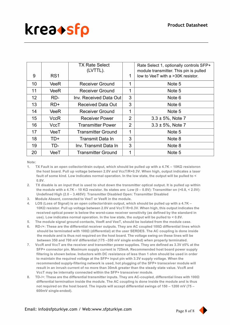
9
RS1
TX Rate Select (LVTTL).
1
Rate Select 1, optionally controls SFP+ module transmitter. This pin is pulled low to VeeT with a >30K resistor.
10 VeeR Receiver Ground 1 Note 5 11 VeeR Receiver Ground 1 Note 5 12 RD- Inv. Received Data Out 3 Note 6 13 RD+ Received Data Out 3 Note 6 14 VeeR Receiver Ground 1 Note 5 15 VccR Receiver Power 2 3.3 ± 5%, Note 7 16 VccT Transmitter Power 2 3.3 ± 5%, Note 7 17 VeeT Transmitter Ground 1 Note 5 18 TD+ Transmit Data In 3 Note 8 19 TD- Inv. Transmit Data In 3 Note 8 20 VeeT Transmitter Ground 1 Note 5
Note: 1. TX Fault is an open collector/drain output, which should be pulled up with a 4.7K – 10KΩ resistoron
the host board. Pull up voltage between 2.0V and VccT/R+0.3V. When high, output indicates a laser fault of some kind. Low indicates normal operation. In the low state, the output will be pulled to < 0.8V.
2. TX disable is an input that is used to shut down the transmitter optical output. It is pulled up within the module with a 4.7K – 10 KΩ resistor. Its states are: Low (0 – 0.8V): Transmitter on (>0.8, < 2.0V): Undefined High (2.0 – 3.465V): Transmitter Disabled Open: Transmitter Disabled
3. Module Absent, connected to VeeT or VeeR in the module. 4. LOS (Loss of Signal) is an open collector/drain output, which should be pulled up with a 4.7K –
10KΩ resistor. Pull up voltage between 2.0V and VccT/ R+0.3V. When high, this output indicates the received optical power is below the worst-case receiver sensitivity (as defined by the standard in use). Low indicates normal operation. In the low state, the output will be pulled to < 0.8V.
5. The module signal ground contacts, VeeR and VeeT, should be isolated from the module case. 6. RD-/+: These are the differential receiver outputs. They are AC coupled 100Ω differential lines which
should be terminated with 100Ω (differential) at the user SERDES. The AC coupling is done inside the module and is thus not required on the host board. The voltage swing on these lines will be between 350 and 700 mV differential (175 –350 mV single ended) when properly terminated.
7. VccR and VccT are the receiver and transmitter power supplies. They are defined as 3.3V ±5% at the SFP+ connector pin. Maximum supply current is 725mA. Recommended host board power supply filtering is shown below. Inductors with DC resistance of less than 1 ohm should be used in order to maintain the required voltage at the SFP+ input pin with 3.3V supply voltage. When the recommended supply-filtering network is used, hot plugging of the SFP+ transceiver module will result in an inrush current of no more than 30mA greater than the steady state value. VccR and VccT may be internally connected within the SFP+ transceiver module.
8. TD-/+: These are the differential transmitter inputs. They are AC-coupled, differential lines with 100Ω differential termination inside the module. The AC coupling is done inside the module and is thus not required on the host board. The inputs will accept differential swings of 150 – 1200 mV (75 – 600mV single-ended).
Page 9 of 8
Product Datasheet
Email: [email protected] / Web:www.sfpturkiye.com
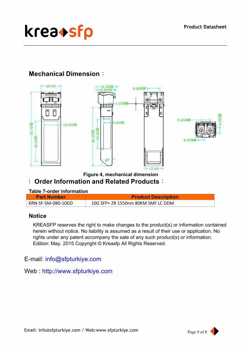
Mechanical Dimension:
Figure 4, mechanical dimension l Order Information and Related Products:
Table 7-order information
Part Number Product Description KRN-SF-SM-080-10GD
10GSFP+ZR1550nm80KMSMFLCDDM
Notice
KREASFP reserves the right to make changes to the product(s) or information contained herein without notice. No liability is assumed as a result of their use or application. No rights under any patent accompany the sale of any such product(s) or information. Edition: May. 2015 Copyright © Kreasfp All Rights Reserved.
E-mail: [email protected]
Web : http://www.sfpturkiye.com