IRFP640 - Elcodisdatasheet.elcodis.com/pdf2/92/73/927393/irfp640.pdf · IRFP640 HEXFET® Power...
2
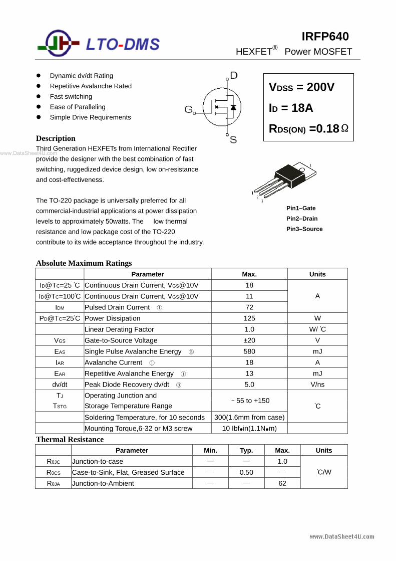
IRFP640 HEXFET ® Power MOSFET z Dynamic dv/dt Rating z Repetitive Avalanche Rated z Fast switching z Ease of Paralleling z Simple Drive Requirements Description Third Generation HEXFETs from International Rectifier VDSS = 200V ID = 18A RDS(ON) =0.18 Ω Pin1–Gate Pin2–Drain Pin3–Source provide the designer with the best combination of fast switching, ruggedized device design, low on-resistance and cost-effectiveness. The TO-220 package is universally preferred for all commercial-industrial applications at power dissipation levels to approximately 50watts. The low thermal resistance and low package cost of the TO-220 contribute to its wide acceptance throughout the industry. Absolute Maximum Ratings Parameter Max. Units ID@TC=25 C Continuous Drain Current, VGS@10V 18 ID@TC=100C Continuous Drain Current, VGS@10V 11 IDM Pulsed Drain Current ① 72 A PD@TC=25C Power Dissipation 125 W Linear Derating Factor 1.0 W/ C VGS Gate-to-Source Voltage ±20 V EAS Single Pulse Avalanche Energy ② 580 mJ IAR Avalanche Current ① 18 A EAR Repetitive Avalanche Energy ① 13 mJ dv/dt Peak Diode Recovery dv/dt ③ 5.0 V/ns TJ TSTG Operating Junction and Storage Temperature Range –55 to +150 Soldering Temperature, for 10 seconds 300(1.6mm from case) C Mounting Torque,6-32 or M3 screw 10 Ibf●in(1.1N●m) Thermal Resistance Parameter Min. Typ. Max. Units RθJC Junction-to-case — — 1.0 RθCS Case-to-Sink, Flat, Greased Surface — 0.50 — RθJA Junction-to-Ambient — — 62 C/W www.DataSheet4U.com
Transcript of IRFP640 - Elcodisdatasheet.elcodis.com/pdf2/92/73/927393/irfp640.pdf · IRFP640 HEXFET® Power...
IRFP640 HEXFET® Power MOSFET
Dynamic dv/dt Rating Repetitive Avalanche Rated Fast switching Ease of Paralleling Simple Drive Requirements
Description Third Generation HEXFETs from International Rectifier
VDSS = 200V
ID = 18A RDS(ON) =0.18Ω
Pin1–Gate
Pin2–Drain
Pin3–Source
provide the designer with the best combination of fast switching, ruggedized device design, low on-resistance and cost-effectiveness. The TO-220 package is universally preferred for all commercial-industrial applications at power dissipation levels to approximately 50watts. The low thermal resistance and low package cost of the TO-220 contribute to its wide acceptance throughout the industry. Absolute Maximum Ratings
Parameter Max. Units ID@TC=25 C Continuous Drain Current, VGS@10V 18 ID@TC=100C Continuous Drain Current, VGS@10V 11
IDM Pulsed Drain Current ① 72 A
PD@TC=25C Power Dissipation 125 W Linear Derating Factor 1.0 W/ C
VGS Gate-to-Source Voltage ±20 V EAS Single Pulse Avalanche Energy ② 580 mJ IAR Avalanche Current ① 18 A EAR Repetitive Avalanche Energy ① 13 mJ
dv/dt Peak Diode Recovery dv/dt ③ 5.0 V/ns TJ
TSTG Operating Junction and Storage Temperature Range –55 to +150
Soldering Temperature, for 10 seconds 300(1.6mm from case) C
Mounting Torque,6-32 or M3 screw 10 Ibfin(1.1Nm) Thermal Resistance
Parameter Min. Typ. Max. Units RθJC Junction-to-case — — 1.0 RθCS Case-to-Sink, Flat, Greased Surface — 0.50 — RθJA Junction-to-Ambient — — 62
C/W
www.DataSheet4U.com
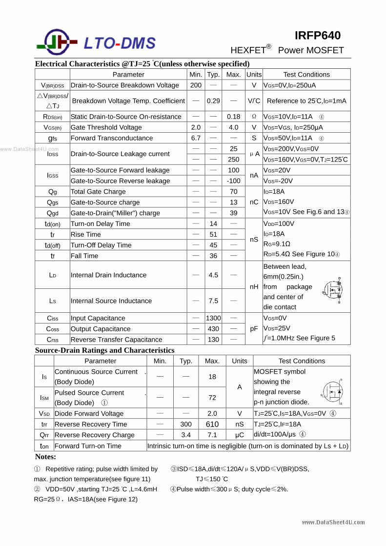
IRFP640 HEXFET® Power MOSFET
Electrical Characteristics @TJ=25 C(unless otherwise specified) Parameter Min. Typ. Max. Units Test Conditions
V(BR)DSS Drain-to-Source Breakdown Voltage 200 — — V VGS=0V,ID=250uA V(BR)DSS/
TJ Breakdown Voltage Temp. Coefficient — 0.29 — V/C Reference to 25C,ID=1mA
RDS(on) Static Drain-to-Source On-resistance — — 0.18 Ω VGS=10V,ID=11A ④ VGS(th) Gate Threshold Voltage 2.0 — 4.0 V VDS=VGS, ID=250μA
gfs Forward Transconductance 6.7 — — S VDS=50V,ID=11A ④ — — 25 VDS=200V,VGS=0V
IDSS Drain-to-Source Leakage current — — 250
μAVDS=160V,VGS=0V,TJ=125C
Gate-to-Source Forward leakage — — 100 VGS=20V IGSS
Gate-to-Source Reverse leakage — — -100nA
VGS=-20V Qg Total Gate Charge — — 70 Qgs Gate-to-Source charge — — 13 Qgd Gate-to-Drain("Miller") charge — — 39
nCID=18A VDS=160V VGS=10V See Fig.6 and 13④
td(on) Turn-on Delay Time — 14 — tr Rise Time — 51 —
td(off) Turn-Off Delay Time — 45 — tf Fall Time — 36 —
nS
VDD=100V ID=18A RG=9.1Ω RD=5.4Ω See Figure 10④
LD Internal Drain Inductance — 4.5 —
LS Internal Source Inductance — 7.5 —
nH
Between lead, 6mm(0.25in.) from package and center of die contact
Ciss Input Capacitance — 1300 — Coss Output Capacitance — 430 — Crss Reverse Transfer Capacitance — 130 —
pFVGS=0V VDS=25V f=1.0MHZ See Figure 5
Source-Drain Ratings and Characteristics Parameter Min. Typ. Max. Units Test Conditions
IS Continuous Source Current . (Body Diode) — — 18
ISM Pulsed Source Current . (Body Diode) ① — — 72
A
MOSFET symbol showing the integral reverse p-n junction diode.
VSD Diode Forward Voltage — — 2.0 V TJ=25C,IS=18A,VGS=0V ④ trr Reverse Recovery Time — 300 610 nS Qrr Reverse Recovery Charge — 3.4 7.1 μC
TJ=25C,IF=18A di/dt=100A/μs ④
ton Forward Turn-on Time Intrinsic turn-on time is negligible (turn-on is dominated by Ls + LD)Notes: ① Repetitive rating; pulse width limited by ③ISD≤18A,di/dt≤120A/μS,VDD≤V(BR)DSS, max. junction temperature(see figure 11) TJ≤150 C ② VDD=50V ,starting TJ=25 C ,L=4.6mH ④Pulse width≤300μS; duty cycle≤2%. RG=25Ω,IAS=18A(see Figure 12)
www.DataSheet4U.com