Industrial Imaging Solutions - PerkinElmer | For The ... · 40 kV - 225 kV (XRD 3025N-G22) 40 kV -...
4
SPECIFICATIONS Features and Benefits • Based on CMOS or a-Si technology • Outstanding image quality • High dynamic range and high resolution • High DQE at low dose • High speed, low noise X-ray detectors with excellent sensitivity • Various scintillator and interface options available 1207NDT Pixel Size 74.8 µm Pixel Matrix 1536 × 864 Active Area 114.9 mm × 64.6 mm Energy 12 kV - 160 kV Speed up to 191 fps Scintillator CsI:Tl or various Gd 2 O 2 S:Tb Technology CMOS Applications • Electronics inspection • Industrial Non-Destructive Testing • Life and physical science 1512NDT Pixel Size 74.8 µm Pixel Matrix 1944 × 1536 Active Area 145.4 mm × 114.9 mm Energy 12 kV - 160 kV Speed up to 86 fps Scintillator CsI:Tl or various Gd 2 O 2 S:Tb Technology CMOS Applications • Electronics inspection • Industrial Non-Destructive Testing • 3D cone beam CT • Life and physical science 2315NDT Pixel Size 74.8 µm Pixel Matrix 3072 × 1944 Active Area 229.8 mm × 145.4 mm Energy 12 kV - 225 kV Speed up to 86 fps Scintillator CsI:Tl or various Gd 2 O 2 S:Tb Technology CMOS Applications • Electronics inspection • Industrial Non-Destructive Testing • 3D cone beam CT • Life and physical science 2923NDT Pixel Size 74.8 µm Pixel Matrix 3888 × 3072 Active Area 290.8 mm × 229.8 mm Energy 12 kV - 225 kV Speed up to 86 fps Scintillator CsI:Tl or various Gd 2 O 2 S:Tb Technology CMOS Applications • Electronics inspection • Industrial Non-Destructive Testing • 3D cone beam CT • Life and physical science Dexela CMOS Detectors Flat Panel X-ray Detectors Industrial Imaging Solutions
Transcript of Industrial Imaging Solutions - PerkinElmer | For The ... · 40 kV - 225 kV (XRD 3025N-G22) 40 kV -...
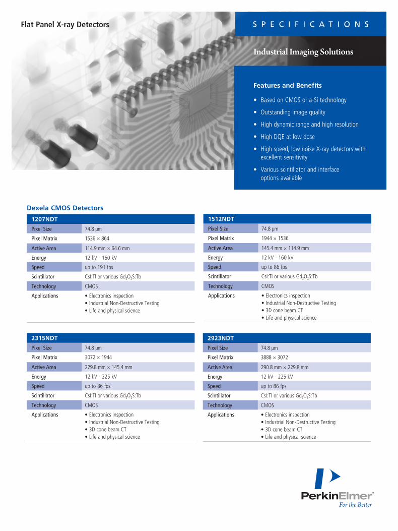
S P E C I F I C A T I O N S
Features and Benefits
• Based on CMOS or a-Si technology
• Outstanding image quality
• High dynamic range and high resolution
• High DQE at low dose
• High speed, low noise X-ray detectors with excellent sensitivity
• Various scintillator and interface options available
1207NDT
Pixel Size 74.8 µm
Pixel Matrix 1536 × 864
Active Area 114.9 mm × 64.6 mm
Energy 12 kV - 160 kV
Speed up to 191 fps
Scintillator CsI:Tl or various Gd2O2S:Tb
Technology CMOS
Applications • Electronics inspection • Industrial Non-Destructive Testing • Life and physical science
1512NDT
Pixel Size 74.8 µm
Pixel Matrix 1944 × 1536
Active Area 145.4 mm × 114.9 mm
Energy 12 kV - 160 kV
Speed up to 86 fps
Scintillator CsI:Tl or various Gd2O2S:Tb
Technology CMOS
Applications • Electronics inspection • Industrial Non-Destructive Testing • 3D cone beam CT • Life and physical science
2315NDT
Pixel Size 74.8 µm
Pixel Matrix 3072 × 1944
Active Area 229.8 mm × 145.4 mm
Energy 12 kV - 225 kV
Speed up to 86 fps
Scintillator CsI:Tl or various Gd2O2S:Tb
Technology CMOS
Applications • Electronics inspection • Industrial Non-Destructive Testing • 3D cone beam CT • Life and physical science
2923NDT
Pixel Size 74.8 µm
Pixel Matrix 3888 × 3072
Active Area 290.8 mm × 229.8 mm
Energy 12 kV - 225 kV
Speed up to 86 fps
Scintillator CsI:Tl or various Gd2O2S:Tb
Technology CMOS
Applications • Electronics inspection • Industrial Non-Destructive Testing • 3D cone beam CT • Life and physical science
Dexela CMOS Detectors
Flat Panel X-ray Detectors
Industrial Imaging Solutions
2
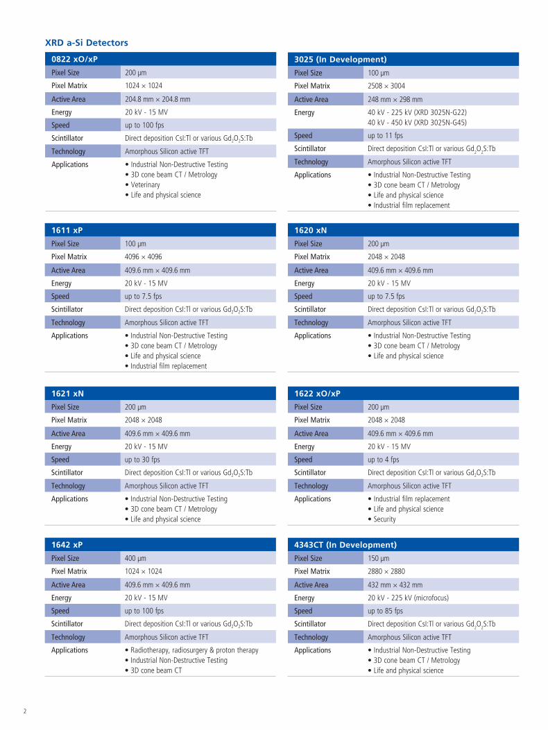
3025 (In Development)
Pixel Size 100 μm
Pixel Matrix 2508 × 3004
Active Area 248 mm × 298 mm
Energy 40 kV - 225 kV (XRD 3025N-G22) 40 kV - 450 kV (XRD 3025N-G45)
Speed up to 11 fps
Scintillator Direct deposition CsI:Tl or various Gd2O2S:Tb
Technology Amorphous Silicon active TFT
Applications • Industrial Non-Destructive Testing • 3D cone beam CT / Metrology • Life and physical science • Industrial film replacement
4343CT (In Development)
Pixel Size 150 µm
Pixel Matrix 2880 × 2880
Active Area 432 mm × 432 mm
Energy 20 kV - 225 kV (microfocus)
Speed up to 85 fps
Scintillator Direct deposition CsI:Tl or various Gd2O2S:Tb
Technology Amorphous Silicon active TFT
Applications • Industrial Non-Destructive Testing • 3D cone beam CT / Metrology • Life and physical science
1620 xN
Pixel Size 200 μm
Pixel Matrix 2048 × 2048
Active Area 409.6 mm × 409.6 mm
Energy 20 kV - 15 MV
Speed up to 7.5 fps
Scintillator Direct deposition CsI:Tl or various Gd2O2S:Tb
Technology Amorphous Silicon active TFT
Applications • Industrial Non-Destructive Testing • 3D cone beam CT / Metrology • Life and physical science
1621 xN
Pixel Size 200 μm
Pixel Matrix 2048 × 2048
Active Area 409.6 mm × 409.6 mm
Energy 20 kV - 15 MV
Speed up to 30 fps
Scintillator Direct deposition CsI:Tl or various Gd2O2S:Tb
Technology Amorphous Silicon active TFT
Applications • Industrial Non-Destructive Testing • 3D cone beam CT / Metrology • Life and physical science
0822 xO/xP
Pixel Size 200 μm
Pixel Matrix 1024 × 1024
Active Area 204.8 mm × 204.8 mm
Energy 20 kV - 15 MV
Speed up to 100 fps
Scintillator Direct deposition CsI:Tl or various Gd2O2S:Tb
Technology Amorphous Silicon active TFT
Applications • Industrial Non-Destructive Testing • 3D cone beam CT / Metrology • Veterinary • Life and physical science
1611 xP
Pixel Size 100 μm
Pixel Matrix 4096 × 4096
Active Area 409.6 mm × 409.6 mm
Energy 20 kV - 15 MV
Speed up to 7.5 fps
Scintillator Direct deposition CsI:Tl or various Gd2O2S:Tb
Technology Amorphous Silicon active TFT
Applications • Industrial Non-Destructive Testing • 3D cone beam CT / Metrology • Life and physical science • Industrial film replacement
XRD a-Si Detectors
1622 xO/xP
Pixel Size 200 μm
Pixel Matrix 2048 × 2048
Active Area 409.6 mm × 409.6 mm
Energy 20 kV - 15 MV
Speed up to 4 fps
Scintillator Direct deposition CsI:Tl or various Gd2O2S:Tb
Technology Amorphous Silicon active TFT
Applications • Industrial film replacement • Life and physical science • Security
1642 xP
Pixel Size 400 μm
Pixel Matrix 1024 × 1024
Active Area 409.6 mm × 409.6 mm
Energy 20 kV - 15 MV
Speed up to 100 fps
Scintillator Direct deposition CsI:Tl or various Gd2O2S:Tb
Technology Amorphous Silicon active TFT
Applications • Radiotherapy, radiosurgery & proton therapy • Industrial Non-Destructive Testing • 3D cone beam CT
3
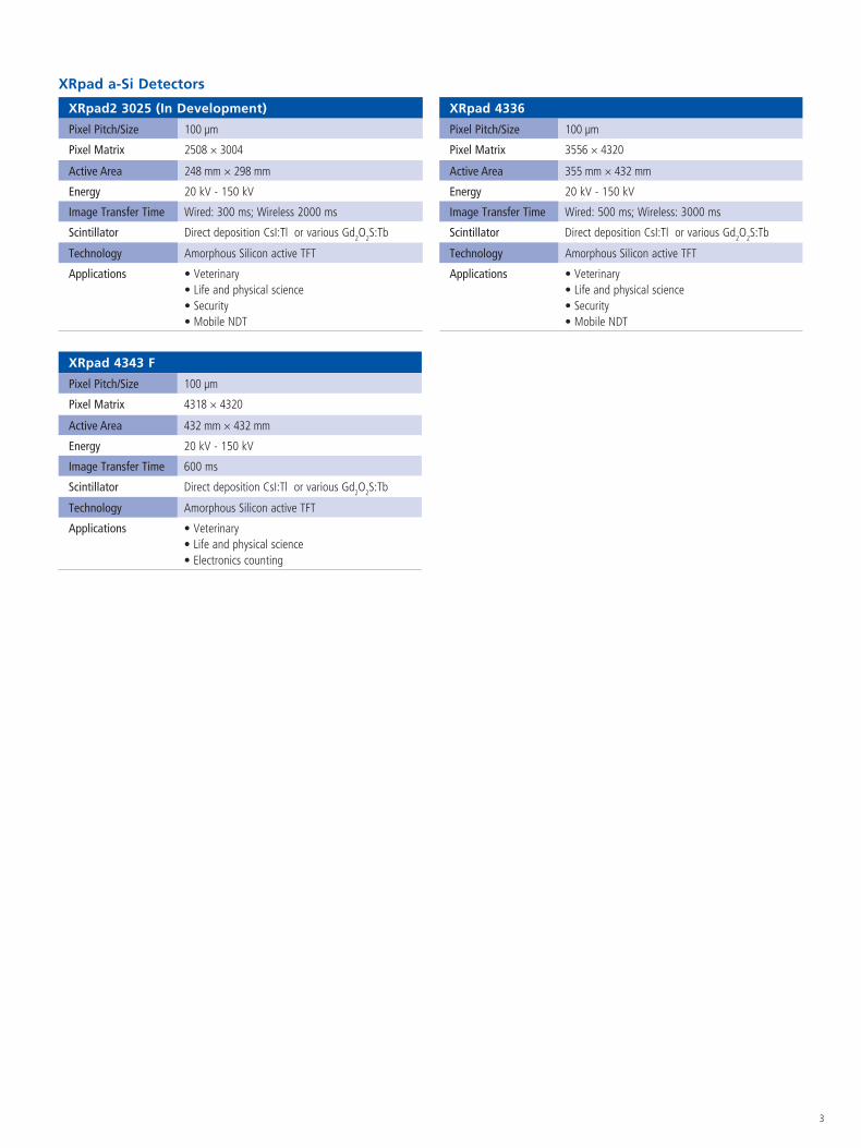
XRpad 4343 F
Pixel Pitch/Size 100 μm
Pixel Matrix 4318 × 4320
Active Area 432 mm × 432 mm
Energy 20 kV - 150 kV
Image Transfer Time 600 ms
Scintillator Direct deposition CsI:Tl or various Gd2O2S:Tb
Technology Amorphous Silicon active TFT
Applications • Veterinary • Life and physical science • Electronics counting
XRpad2 3025 (In Development)
Pixel Pitch/Size 100 μm
Pixel Matrix 2508 × 3004
Active Area 248 mm × 298 mm
Energy 20 kV - 150 kV
Image Transfer Time Wired: 300 ms; Wireless 2000 ms
Scintillator Direct deposition CsI:Tl or various Gd2O2S:Tb
Technology Amorphous Silicon active TFT
Applications • Veterinary • Life and physical science • Security • Mobile NDT
XRpad 4336
Pixel Pitch/Size 100 μm
Pixel Matrix 3556 × 4320
Active Area 355 mm × 432 mm
Energy 20 kV - 150 kV
Image Transfer Time Wired: 500 ms; Wireless: 3000 ms
Scintillator Direct deposition CsI:Tl or various Gd2O2S:Tb
Technology Amorphous Silicon active TFT
Applications • Veterinary • Life and physical science • Security • Mobile NDT
XRpad a-Si Detectors

For a complete listing of our global offices, visit www.perkinelmer.com/ContactUs
Copyright ©2015-2016, PerkinElmer, Inc. All rights reserved. PerkinElmer® is a registered trademark of PerkinElmer, Inc. All other trademarks are the property of their respective owners. 012163A_01 PKI
USA PerkinElmer, Inc.2175 Mission College BlvdSanta Clara, CA 95054 USAP: +1-844-726-8228F: +1-408-969-6493
GermanyPerkinElmer Technologies GmbH & Co. KGIn der Rehbach 22 65396 Walluf Germany P: +49-6123-971-300 F: +49-6123-971-600
United Kingdom Dexela LimitedA PerkinElmer CompanyWenlock Business Centre50-52 Wharf RoadLondon N1 7EU United KingdomP: +44-20-7148-3107
ChinaPerkinElmer, Inc.No. 1670 Zhangheng Road Zhangjiang Hi-Tech Park Shanghai 201203, PRC P: +86-21-6064-5611 F: +86-21-6064-5666
Visit our website at www.perkinelmer.com/imaging-components/ and contact us through the contact form provided or email [email protected].