High Responsivity and High Rejection Ratio of Self-Powered...
7
High Responsivity and High Rejection Ratio of Self-Powered Solar- Blind Ultraviolet Photodetector Based on PEDOT:PSS/β-Ga 2 O 3 Organic/Inorganic p−n Junction Hebin Wang, #,† Hongyu Chen,* ,#,† Li Li, ⊥,# Yuefei Wang, † Longxing Su, ‡ Wanpeng Bian, † Bingsheng Li,* ,§ and Xiaosheng Fang* ,∥ † Department of Physics, Harbin Institute of Technology, Harbin 150001, P. R. China ⊥ School of Life Science and Technology, Harbin Institute of Technology, Harbin 150080, P. R. China ‡ Department of Physical Science and Technology, ShanghaiTech University, Shanghai 201210, P. R. China § Center for Advanced Optoelectronic Functional Materials Research, Key Laboratory of UV-Emitting Materials and Technology of Ministry of Education, Northeast Normal University, Changchun 130024, P. R. China ∥ Department of Materials Science, Fudan University, Shanghai 200433, P. R. China * S Supporting Information ABSTRACT: A high responsivity self-powered solar-blind deep UV (DUV) photo- detector with high rejection ratio was proposed based on inorganic/organic hybrid p−n junction. Owing to the high crystallized β-Ga 2 O 3 and excellent transparent conductive polymer PEDOT:PSS, the device exhibited ultrahigh responsivity of 2.6 A/W at 245 nm with a sharp cutoff wavelength at 255 nm without any power supply. The responsivity is much larger than that of previous solar-blind DUV photodetectors. Moreover, the device exhibited an ultrahigh solar-blind/UV rejection ratio (R 245 nm /R 280 nm ) of 10 3 , which is two orders of magnitude larger than the average value reported in Ga 2 O 3 -based solar-blind photodetectors. In addition, the photodetector shows a narrow bandpass response of only 17 nm in width. This work might be of great value in developing a high wavelength selective DUV photodetector with respect to low cost for future energy-efficient photoelectric devices. P hotodetectors operating in deep-ultraviolet (DUV) solar- blind region (220−280 nm) avoiding interference from solar radiation have drawn extensive attention in the past few decades. Especially DUV photodetectors with high wavelength selectivity exhibited many potential significant applications in missile warning, fire alarms, medical insurance, environmental monitoring, space-to-space communications, etc. 1−5 Therefore, to achieve desirable photodetection, much efforts have been carried out for constructing DUV photodetectors with high responsivity and high rejection ratio up to now. Benefited from sophisticated fabrication technologies such as molecular beam epitaxy (MBE) and metal−organic chemical vapor deposition (MOCVD), versatile wavelength selective DUV photodetec- tors with high performance have been fabricated by the successful utilization of band gap engineering, and high crystal quality alloy wide bandgap semiconductors such as GaAlN, MgZnO, BeZnO with tunable bandgap have been explored extensively. 6−11 However, the defect density of GaAlN increases remarkably with increasing the Al composition in the alloy thin film, which would severely limit these materials applications in DUV region. Although MgZnO alloys with a tunable band gap in the solar-blind region, phase-separation will occur in MgZnO alloys at a certain Mg composition. Because MgO prefers to crystallize in cubic rocksalt structure, while ZnO prefers to crystallize in hexagonal wurtzite structure. 12 Coincidentally, phase segregation of BeZnO will also occur if Be composition is relatively high. This can be ascribed to the large lattice mismatch between BeO and ZnO, and the tremendous ionic radius difference between Zn 2+ (0.6 Å) and Be 2+ (0.27 Å). 13 Therefore, various defects in these alloy semiconductors seriously influenced the cut off wave- length and signal-noise ratio of photodetectors in solar-blind region. In addition, to achieve a desirable photodetection long- term working in some unmanned hazardous atmosphere or harsh environment, high responsivity and high wavelength selectivity self-powered DUV photodetectors capable of operating without any power supply are urgently needed. In spite of alloy semiconductors, ultrawide bandgap semiconductors such as diamond, BN, and Ga 2 O 3 have been developed in fabricating solar-blind photodetectors re- cently. 14−18 Among these materials, Ga 2 O 3 has been extensively studied as an important n-type semiconductor in solar-blind photodetectors owing to its distinct DUV absorption characteristics (>10 5 cm −1 near band edge) with Received: September 22, 2019 Accepted: October 18, 2019 Published: October 18, 2019 Letter pubs.acs.org/JPCL Cite This: J. Phys. Chem. Lett. 2019, 10, 6850-6856 © 2019 American Chemical Society 6850 DOI: 10.1021/acs.jpclett.9b02793 J. Phys. Chem. Lett. 2019, 10, 6850−6856 Downloaded via FUDAN UNIV on December 13, 2019 at 06:28:32 (UTC). See https://pubs.acs.org/sharingguidelines for options on how to legitimately share published articles.
Transcript of High Responsivity and High Rejection Ratio of Self-Powered...
High Responsivity and High Rejection Ratio of Self-Powered Solar-Blind Ultraviolet Photodetector Based on PEDOT:PSS/β-Ga2O3Organic/Inorganic p−n JunctionHebin Wang,#,† Hongyu Chen,*,#,† Li Li,⊥,# Yuefei Wang,† Longxing Su,‡ Wanpeng Bian,†
Bingsheng Li,*,§ and Xiaosheng Fang*,∥
†Department of Physics, Harbin Institute of Technology, Harbin 150001, P. R. China⊥School of Life Science and Technology, Harbin Institute of Technology, Harbin 150080, P. R. China‡Department of Physical Science and Technology, ShanghaiTech University, Shanghai 201210, P. R. China§Center for Advanced Optoelectronic Functional Materials Research, Key Laboratory of UV-Emitting Materials and Technology ofMinistry of Education, Northeast Normal University, Changchun 130024, P. R. China∥Department of Materials Science, Fudan University, Shanghai 200433, P. R. China
*S Supporting Information
ABSTRACT: A high responsivity self-powered solar-blind deep UV (DUV) photo-detector with high rejection ratio was proposed based on inorganic/organic hybrid p−njunction. Owing to the high crystallized β-Ga2O3 and excellent transparent conductivepolymer PEDOT:PSS, the device exhibited ultrahigh responsivity of 2.6 A/W at 245 nmwith a sharp cutoff wavelength at 255 nm without any power supply. The responsivity ismuch larger than that of previous solar-blind DUV photodetectors. Moreover, the deviceexhibited an ultrahigh solar-blind/UV rejection ratio (R245 nm/R280 nm) of 10
3, which is twoorders of magnitude larger than the average value reported in Ga2O3-based solar-blindphotodetectors. In addition, the photodetector shows a narrow bandpass response of only17 nm in width. This work might be of great value in developing a high wavelengthselective DUV photodetector with respect to low cost for future energy-efficientphotoelectric devices.
Photodetectors operating in deep-ultraviolet (DUV) solar-blind region (220−280 nm) avoiding interference from
solar radiation have drawn extensive attention in the past fewdecades. Especially DUV photodetectors with high wavelengthselectivity exhibited many potential significant applications inmissile warning, fire alarms, medical insurance, environmentalmonitoring, space-to-space communications, etc.1−5 Therefore,to achieve desirable photodetection, much efforts have beencarried out for constructing DUV photodetectors with highresponsivity and high rejection ratio up to now. Benefited fromsophisticated fabrication technologies such as molecular beamepitaxy (MBE) and metal−organic chemical vapor deposition(MOCVD), versatile wavelength selective DUV photodetec-tors with high performance have been fabricated by thesuccessful utilization of band gap engineering, and high crystalquality alloy wide bandgap semiconductors such as GaAlN,MgZnO, BeZnO with tunable bandgap have been exploredextensively.6−11 However, the defect density of GaAlNincreases remarkably with increasing the Al composition inthe alloy thin film, which would severely limit these materialsapplications in DUV region. Although MgZnO alloys with atunable band gap in the solar-blind region, phase-separationwill occur in MgZnO alloys at a certain Mg composition.Because MgO prefers to crystallize in cubic rocksalt structure,
while ZnO prefers to crystallize in hexagonal wurtzitestructure.12 Coincidentally, phase segregation of BeZnO willalso occur if Be composition is relatively high. This can beascribed to the large lattice mismatch between BeO and ZnO,and the tremendous ionic radius difference between Zn2+(0.6Å) and Be2+(0.27 Å).13 Therefore, various defects in thesealloy semiconductors seriously influenced the cut off wave-length and signal-noise ratio of photodetectors in solar-blindregion. In addition, to achieve a desirable photodetection long-term working in some unmanned hazardous atmosphere orharsh environment, high responsivity and high wavelengthselectivity self-powered DUV photodetectors capable ofoperating without any power supply are urgently needed.In spite of alloy semiconductors, ultrawide bandgap
semiconductors such as diamond, BN, and Ga2O3 have beendeveloped in fabricating solar-blind photodetectors re-cently.14−18 Among these materials, Ga2O3 has beenextensively studied as an important n-type semiconductor insolar-blind photodetectors owing to its distinct DUVabsorption characteristics (>105 cm−1 near band edge) with
Received: September 22, 2019Accepted: October 18, 2019Published: October 18, 2019
Letter
pubs.acs.org/JPCLCite This: J. Phys. Chem. Lett. 2019, 10, 6850−6856
© 2019 American Chemical Society 6850 DOI: 10.1021/acs.jpclett.9b02793J. Phys. Chem. Lett. 2019, 10, 6850−6856
Dow
nloa
ded
via
FUD
AN
UN
IV o
n D
ecem
ber
13, 2
019
at 0
6:28
:32
(UT
C).
See
http
s://p
ubs.
acs.
org/
shar
ingg
uide
lines
for
opt
ions
on
how
to le
gitim
atel
y sh
are
publ
ishe
d ar
ticle
s.
a wide bandgap (∼4.9 eV), which is promising for develop-ment of DUV photodetectors.19−22 Moreover, β-Ga2O3 usuallyexhibit high chemical and thermal stability, larger electronmobility, and lower defect concentration, which is favorable forfabricating high performance photodetectors working in harshenvironments. Up to now, due to the difficulty of realizing thep−n homojunction and vertical Schottky Ga2O3 photodiodes,great efforts in fabricating Ga2O3 based self-powered photo-detectors have been proposed through the construction ofheterojunctions in conjunction with ZnO, GaN, MoS2,etc.20,23−26 Although several photodetectors possess highresponsivity in the solar-blind region, the cutoff wavelengthand rejection ratio of these devices are seriously affected by therelatively narrow band gap semiconductors. Therefore, thecomprehensive performance of solar-blind photodetectors isstill lower than expected.Fortunately, the emergence of organic conductive polymers
provide us an additional pathway for fabricating photovoltaicdevices owing to their several unique properties, such as easyprocessing, low cost, high flexibility, conjugated π-electrons inthe polymer backbone, high stability, etc. In particular,PEDOT:PSS is an excellent p-type conductive polymer, itselectrical conductivity could reach more than 1000 s·cm−1.27−30 In spite of this, the electrical conductivities ofPEDOT:PSS could be tailored over many orders of magnitudeby changing its dopant type and oxidation state. Our and otherprevious works indicated that PEDOT:PSS is a suitableplatform to construct photodetectors as an excellent holetransporting layer.28−31 Therefore, in conjunction with thehigh crystallized Ga2O3 microwire, an ultrahigh responsivity(2.6 A/W) self-powered solar-blind photodetector with a sharpcutoff wavelength of 255 nm was proposed based on thePEDOT:PSS/Ga2O3 organic−inorganic hybrid p−n junction(Figure 1). It is worth pointing out that the device exhibited an
ultrahigh solar-blind/UV rejection ratio (245/280 nm) of 103.This value is almost two orders of magnitude larger than thatof Ga2O3 based self-powered photodetector.21,26,32 Its UV/visible (245/400 nm) rejection ratio could achieve up to ∼9 ×10⁴, which is comparable to that of previous excellent solar-blind photodetectors even at a bias voltage.2,14 Moreover, thephotodetector based on PEDOT:PSS/Ga2O3 heterojunctionshows a narrow response “window” of only 17 nm, and a highwavelength selectivity photodetector was obtained, as well.This work will be an important exploration in developing highperformance self-powered DUV photodetectors.Figure 2a is the optical image of Ga2O3 single microwires. It
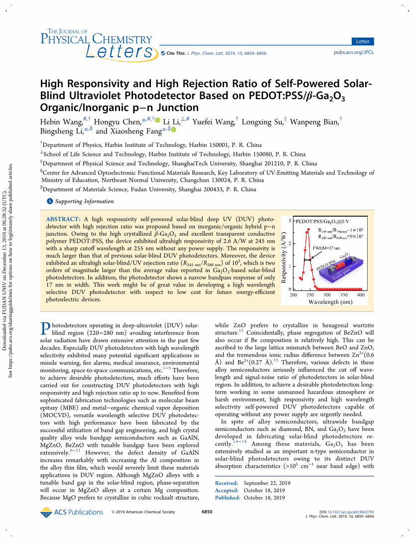
can be found that the microwires are ranging in length from 6to 9 mm, and the longest length of the microwire could reach
up to 1 cm. The cross section of scanning electron microscopy(SEM) and low-magnification transmission electron micros-copy (TEM) images of the Ga2O3 microwire demonstrate thatthe microwires are quadrangular with the average diameter ofabout 10 μm (Figures 2b,c and S2). At the same time, the SEMimage shows a smooth surface of Ga2O3 microwires. Figure 2dis the selected area electron diffraction (SAED) pattern andhigh-resolution TEM (HRTEM) image of Ga2O3 microwire.From the SAED pattern image, the as-fabricated Ga2O3microwires have a monoclinic lattice structure with the [010]zone axis. The lattice constant along the [010] direction is 0.30nm, the d-spacing of {001} plane family is 0.55 nm, and theangle between (010) and (001) crystallographic planes is 90°.These results are corresponding well to the monoclinic latticeof β-Ga2O3 (a = 12.23 Å, b = 3.04 Å, c = 5.80 Å).Raman spectrum and FTIR spectrum were performed to
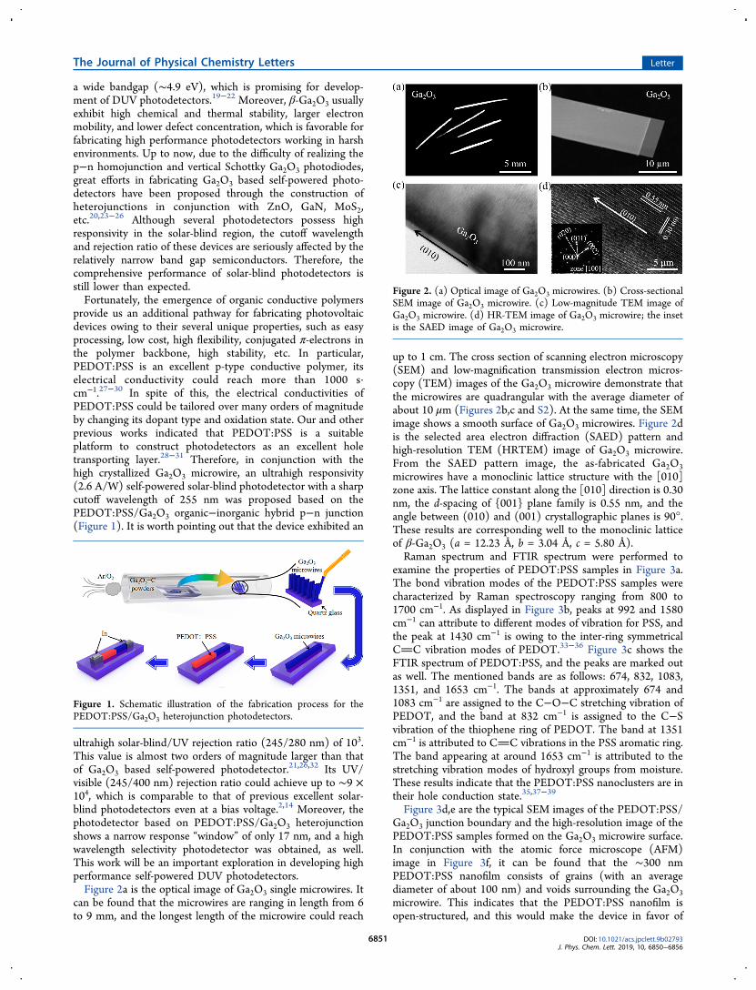
examine the properties of PEDOT:PSS samples in Figure 3a.The bond vibration modes of the PEDOT:PSS samples werecharacterized by Raman spectroscopy ranging from 800 to1700 cm−1. As displayed in Figure 3b, peaks at 992 and 1580cm−1 can attribute to different modes of vibration for PSS, andthe peak at 1430 cm−1 is owing to the inter-ring symmetricalCC vibration modes of PEDOT.33−36 Figure 3c shows theFTIR spectrum of PEDOT:PSS, and the peaks are marked outas well. The mentioned bands are as follows: 674, 832, 1083,1351, and 1653 cm−1. The bands at approximately 674 and1083 cm−1 are assigned to the C−O−C stretching vibration ofPEDOT, and the band at 832 cm−1 is assigned to the C−Svibration of the thiophene ring of PEDOT. The band at 1351cm−1 is attributed to CC vibrations in the PSS aromatic ring.The band appearing at around 1653 cm−1 is attributed to thestretching vibration modes of hydroxyl groups from moisture.These results indicate that the PEDOT:PSS nanoclusters are intheir hole conduction state.35,37−39
Figure 3d,e are the typical SEM images of the PEDOT:PSS/Ga2O3 junction boundary and the high-resolution image of thePEDOT:PSS samples formed on the Ga2O3 microwire surface.In conjunction with the atomic force microscope (AFM)image in Figure 3f, it can be found that the ∼300 nmPEDOT:PSS nanofilm consists of grains (with an averagediameter of about 100 nm) and voids surrounding the Ga2O3microwire. This indicates that the PEDOT:PSS nanofilm isopen-structured, and this would make the device in favor of
Figure 1. Schematic illustration of the fabrication process for thePEDOT:PSS/Ga2O3 heterojunction photodetectors.
Figure 2. (a) Optical image of Ga2O3 microwires. (b) Cross-sectionalSEM image of Ga2O3 microwire. (c) Low-magnitude TEM image ofGa2O3 microwire. (d) HR-TEM image of Ga2O3 microwire; the insetis the SAED image of Ga2O3 microwire.
The Journal of Physical Chemistry Letters Letter
DOI: 10.1021/acs.jpclett.9b02793J. Phys. Chem. Lett. 2019, 10, 6850−6856
6851
yielding higher quantum efficiency and longer photocarrierlifetime due to surface states.In order to explore the usefulness of the PEDOT:PSS/
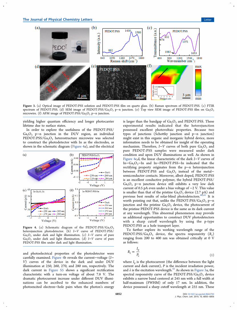
Ga2O3 p−n junction in the DUV region, an individualPEDOT:PSS/Ga2O3 heterostructure microwire was selectedto construct the photodetector with In as the electrodes, asshown in the schematic diagram (Figure 4a), and the electrical
and photoelectrical properties of the photodetector werecarefully examined. Figure 4b reveals the current−voltage (I−V) curves of the device in the dark and under DUVillumination at 250, 260, 270, and 280 nm, respectively. Thedark current in Figure S5 shows a significant rectificationcharacteristic with a turn-on voltage of about 7.8 V. Thedramatic photocurrent increase under different DUV illumi-nations can be ascribed to the enhanced numbers ofphotoexcited electron−hole pairs when the photon’s energy
is larger than the bandgap of Ga2O3 and PEDOT:PSS. Theseexperimental results indicated that the heterojunctionpossessed excellent photovoltaic properties. Because twotypes of junctions (Schottky junction and p−n junction)might exist in this organic and inorganic hybrid device, moreinformation needs to be obtained for insight of the operatingmechanism. Therefore, I−V curves of both pure Ga2O3 andpure PEDOT:PSS samples were measured under darkcondition and upon DUV illuminations as well. As shown inFigure 4c,d, the linear characteristic of the dark I−V curves ofIn−Ga2O3−In and In−PEDOT:PSS−In indicated that therectifying property originates from the p−n heterojunctionbetween PEDOT:PSS and Ga2O3 instead of the metal−semiconductor contacts. Moreover, albeit doped, PEDOT:PSSis an excellent conductive polymer, the hybrid PEDOT:PSS/Ga2O3 p−n junction device still exhibits a very low darkcurrent of 0.5 pA even under a bias voltage of −2 V. This valueis smaller than that of the pristine Ga2O3 device (2.7 pA) andprevious best results of solar-blind photodetectors.40,41 It isworth pointing out that, unlike the PEDOT:PSS/Ga2O3 p−njunction and the pristine Ga2O3 device, the photocurrent ofthe pristine PEDOT:PSS device is the same as its dark currentat any wavelength. This abnormal phenomenon may provideus additional opportunities to construct DUV photodetectorswith a sharp cutoff wavelength by using the p-typePEDOT:PSS as a hole transport layer.To further explore its working wavelength range of the
PEDOT:PSS/Ga2O3 device, the spectra responsivity (Rλ)ranging from 200 to 400 nm was obtained critically at 0 Vas follows:
=λλ
RI
Pp
(1)
where Ip is the photocurrent (the difference between the lightcurrent and dark current), P is the incident irradiation power,and λ is the excitation wavelength.42 As shown in Figure 5a, thespectral responsivity curve of the PEDOT:PSS/Ga2O3 deviceexhibits a narrow band centered at 245 nm with a full width athalf-maximum (FWHM) of only 17 nm. In addition, thedevice possessed a sharp cutoff wavelength at 255 nm. These
Figure 3. (a) Optical image of PEDOT:PSS solution and PEDOT:PSS film on quartz glass. (b) Raman spectrum of PEDOT:PSS. (c) FTIRspectrum of PEDOT:PSS. (d) SEM image of PEDOT:PSS/Ga2O3 p−n junction. (e) Top view SEM image of PEDOT:PSS film on Ga2O3microwire. (f) AFM image of PEDOT:PSS/Ga2O3 p−n junction.
Figure 4. (a) Schematic diagram of the PEDOT:PSS/Ga2O3heterojunction photodetector. (b) I−V curve of PEDOT:PSS/Ga2O3 under dark and light illumination. (c) I−V curve of pureGa2O3 under dark and light illumination. (d) I−V curve of purePEDOT:PSS film under dark and light illumination.
The Journal of Physical Chemistry Letters Letter
DOI: 10.1021/acs.jpclett.9b02793J. Phys. Chem. Lett. 2019, 10, 6850−6856
6852
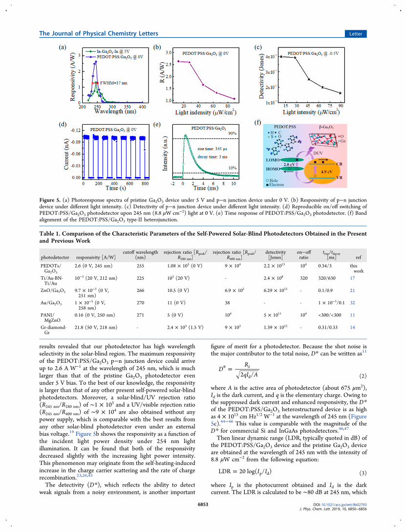
results revealed that our photodetector has high wavelengthselectivity in the solar-blind region. The maximum responsivityof the PEDOT:PSS/Ga2O3 p−n junction device could arriveup to 2.6 A W−1 at the wavelength of 245 nm, which is muchlarger than that of the pristine Ga2O3 photodetector evenunder 5 V bias. To the best of our knowledge, the responsivityis larger than that of any other present self-powered solar-blindphotodetectors. Moreover, a solar-blind/UV rejection ratio(R245 nm/R280 nm) of ∼1 × 10³ and a UV/visible rejection ratio(R245 nm/R400 nm) of ∼9 × 10⁴ are also obtained without anypower supply, which is comparable with the best results fromany other solar-blind photodetector even under an externalbias voltage.14 Figure 5b shows the responsivity as a function ofthe incident light power density under 254 nm lightillumination. It can be found that both of the responsivitydecreased slightly with the increasing light power intensity.This phenomenon may originate from the self-heating-inducedincrease in the charge carrier scattering and the rate of chargerecombination.23,26,43
The detectivity (D*), which reflects the ability to detectweak signals from a noisy environment, is another important
figure of merit for a photodetector. Because the shot noise isthe major contributor to the total noise, D* can be written as11
* = λDRqI A2 /d (2)
where A is the active area of photodetector (about 675 μm2),Id is the dark current, and q is the elementary charge. Owing tothe suppressed dark current and enhanced responsivity, the D*of the PEDOT:PSS/Ga2O3 heterostructured device is as highas 4 × 1013 cm Hz1/2 W−1 at the wavelength of 245 nm (Figure5c).44−46 This value is comparable with the magnitude of theD* for commercial Si and InGaAs photodetectors.46,47
Then linear dynamic range (LDR, typically quoted in dB) ofthe PEDOT:PSS/Ga2O3 device and the pristine Ga2O3 deviceare obtained at the wavelength of 245 nm with the intensity of8.8 μW cm−2 from the following equation:
= I ILDR 20 log( / )p d (3)
where Ip is the photocurrent obtained and Id is the darkcurrent. The LDR is calculated to be ∼80 dB at 245 nm, which
Figure 5. (a) Photoresponse spectra of pristine Ga2O3 device under 5 V and p−n junction device under 0 V. (b) Responsivity of p−n junctiondevice under different light intensity. (c) Detectivity of p−n junction device under different light intensity. (d) Reproducible on/off switching ofPEDOT:PSS/Ga2O3 photodetector upon 245 nm (8.8 μW cm−2) light at 0 V. (e) Time response of PEDOT:PSS/Ga2O3 photodetector. (f) Bandalignment of the PEDOT:PSS/Ga2O3 type-II heterojunction.
Table 1. Comparison of the Characteristic Parameters of the Self-Powered Solar-Blind Photodetectors Obtained in the Presentand Previous Work
photodetector responsivity [A/W]cutoff wavelength
(nm)rejection ratio [Rpeak/
R280 nm]rejection ratio [Rpeak/
R400 nm]detectivity[Jones]
on−offratio
trise/tdecay[ms] ref
PEDOTs/Ga2O3
2.6 (0 V, 245 nm) 255 1.08 × 10³ (0 V) 9 × 10⁴ 2.2 × 10¹³ 104 0.34/3 thiswork
Ti/Au-BN-Ti/Au
10−3 (20 V, 212 nm) 225 103 (20 V) - 2.4 × 10⁸ 320 320/630 17
ZnO/Ga2O3 9.7 × 10⁻³ (0 V,251 nm)
266 10.5 (0 V) 6.9 × 10² 6.29 × 10¹² - 0.1/0.9 21
Au/Ga2O3 1 × 10⁻⁵ (0 V,258 nm)
270 11 (0 V) 38 - - 1 × 10⁻³/0.1 32
PANI/MgZnO
0.16 (0 V, 250 nm) 271 5 (0 V) 104 5 × 10¹¹ 104 <300/<300 11
Gr-diamond-Gr
21.8 (50 V, 218 nm) - 2.4 × 10³ (1.5 V) 9 × 10³ 1.39 × 10¹² - 0.31/0.33 14
The Journal of Physical Chemistry Letters Letter
DOI: 10.1021/acs.jpclett.9b02793J. Phys. Chem. Lett. 2019, 10, 6850−6856
6853
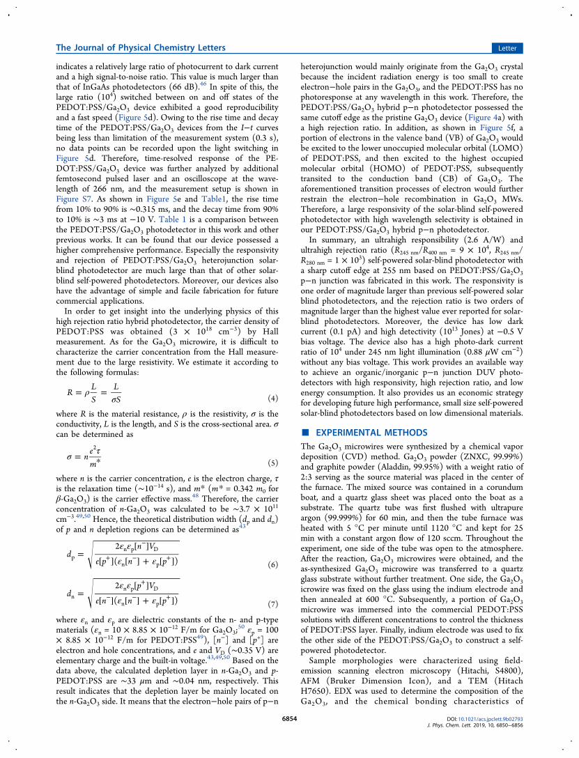
indicates a relatively large ratio of photocurrent to dark currentand a high signal-to-noise ratio. This value is much larger thanthat of InGaAs photodetectors (66 dB).46 In spite of this, thelarge ratio (104) switched between on and off states of thePEDOT:PSS/Ga2O3 device exhibited a good reproducibilityand a fast speed (Figure 5d). Owing to the rise time and decaytime of the PEDOT:PSS/Ga2O3 devices from the I−t curvesbeing less than limitation of the measurement system (0.3 s),no data points can be recorded upon the light switching inFigure 5d. Therefore, time-resolved response of the PE-DOT:PSS/Ga2O3 device was further analyzed by additionalfemtosecond pulsed laser and an oscilloscope at the wave-length of 266 nm, and the measurement setup is shown inFigure S7. As shown in Figure 5e and Table1, the rise timefrom 10% to 90% is ∼0.315 ms, and the decay time from 90%to 10% is ∼3 ms at −10 V. Table 1 is a comparison betweenthe PEDOT:PSS/Ga2O3 photodetector in this work and otherprevious works. It can be found that our device possessed ahigher comprehensive performance. Especially the responsivityand rejection of PEDOT:PSS/Ga2O3 heterojunction solar-blind photodetector are much large than that of other solar-blind self-powered photodetectors. Moreover, our devices alsohave the advantage of simple and facile fabrication for futurecommercial applications.In order to get insight into the underlying physics of this
high rejection ratio hybrid photodetector, the carrier density ofPEDOT:PSS was obtained (3 × 1018 cm−3) by Hallmeasurement. As for the Ga2O3 microwire, it is difficult tocharacterize the carrier concentration from the Hall measure-ment due to the large resistivity. We estimate it according tothe following formulas:
ρσ
= =RLS
LS (4)
where R is the material resistance, ρ is the resistivity, σ is theconductivity, L is the length, and S is the cross-sectional area. σcan be determined as
σ τ= *nem
2
(5)
where n is the carrier concentration, e is the electron charge, τis the relaxation time (∼10−14 s), and m* (m* = 0.342 m0 forβ-Ga2O3) is the carrier effective mass.48 Therefore, the carrierconcentration of n-Ga2O3 was calculated to be ∼3.7 × 10¹¹
cm−3.49,50 Hence, the theoretical distribution width (dp and dn)of p and n depletion regions can be determined as43
ε εε ε
=[ ]
[ ] [ ] + [ ]
−
+ − +dn V
e p n p
2
( )pn p D
n p (6)
ε εε ε
=[ ]
[ ] [ ] + [ ]
+
− − +dp V
e n n p
2
( )nn p D
n p (7)
where εn and εp are dielectric constants of the n- and p-typematerials (εn = 10 × 8.85 × 10−12 F/m for Ga2O3;
50 εp = 100× 8.85 × 10−12 F/m for PEDOT:PSS49), [n−] and [p+] areelectron and hole concentrations, and e and VD (∼0.35 V) areelementary charge and the built-in voltage.43,49,50 Based on thedata above, the calculated depletion layer in n-Ga2O3 and p-PEDOT:PSS are ∼33 μm and ∼0.04 nm, respectively. Thisresult indicates that the depletion layer be mainly located onthe n-Ga2O3 side. It means that the electron−hole pairs of p−n
heterojunction would mainly originate from the Ga2O3 crystalbecause the incident radiation energy is too small to createelectron−hole pairs in the Ga2O3, and the PEDOT:PSS has nophotoresponse at any wavelength in this work. Therefore, thePEDOT:PSS/Ga2O3 hybrid p−n photodetector possessed thesame cutoff edge as the pristine Ga2O3 device (Figure 4a) witha high rejection ratio. In addition, as shown in Figure 5f, aportion of electrons in the valence band (VB) of Ga2O3 wouldbe excited to the lower unoccupied molecular orbital (LOMO)of PEDOT:PSS, and then excited to the highest occupiedmolecular orbital (HOMO) of PEDOT:PSS, subsequentlytransited to the conduction band (CB) of Ga2O3. Theaforementioned transition processes of electron would furtherrestrain the electron−hole recombination in Ga2O3 MWs.Therefore, a large responsivity of the solar-blind self-poweredphotodetector with high wavelength selectivity is obtained inour PEDOT:PSS/Ga2O3 hybrid p−n photodetector.In summary, an ultrahigh responsibility (2.6 A/W) and
ultrahigh rejection ratio (R245 nm/R400 nm = 9 × 10⁴, R245 nm/R280 nm = 1 × 10³) self-powered solar-blind photodetector witha sharp cutoff edge at 255 nm based on PEDOT:PSS/Ga2O3p−n junction was fabricated in this work. The responsivity isone order of magnitude larger than previous self-powered solarblind photodetectors, and the rejection ratio is two orders ofmagnitude larger than the highest value ever reported for solar-blind photodetectors. Moreover, the device has low darkcurrent (0.1 pA) and high detectivity (1013 Jones) at −0.5 Vbias voltage. The device also has a high photo-dark currentratio of 104 under 245 nm light illumination (0.88 μW cm−2)without any bias voltage. This work provides an available wayto achieve an organic/inorganic p−n junction DUV photo-detectors with high responsivity, high rejection ratio, and lowenergy consumption. It also provides us an economic strategyfor developing future high performance, small size self-poweredsolar-blind photodetectors based on low dimensional materials.
■ EXPERIMENTAL METHODSThe Ga2O3 microwires were synthesized by a chemical vapordeposition (CVD) method. Ga2O3 powder (ZNXC, 99.99%)and graphite powder (Aladdin, 99.95%) with a weight ratio of2:3 serving as the source material was placed in the center ofthe furnace. The mixed source was contained in a corundumboat, and a quartz glass sheet was placed onto the boat as asubstrate. The quartz tube was first flushed with ultrapureargon (99.999%) for 60 min, and then the tube furnace washeated with 5 °C per minute until 1120 °C and kept for 25min with a constant argon flow of 120 sccm. Throughout theexperiment, one side of the tube was open to the atmosphere.After the reaction, Ga2O3 microwires were obtained, and theas-synthesized Ga2O3 microwire was transferred to a quartzglass substrate without further treatment. One side, the Ga2O3icrowire was fixed on the glass using the indium electrode andthen annealed at 600 °C. Subsequently, a portion of Ga2O3microwire was immersed into the commercial PEDOT:PSSsolutions with different concentrations to control the thicknessof PEDOT:PSS layer. Finally, indium electrode was used to fixthe other side of the PEDOT:PSS/Ga2O3 to construct a self-powered photodetector.Sample morphologies were characterized using field-
emission scanning electron microscopy (Hitachi, S4800),AFM (Bruker Dimension Icon), and a TEM (HitachH7650). EDX was used to determine the composition of theGa2O3, and the chemical bonding characteristics of
The Journal of Physical Chemistry Letters Letter
DOI: 10.1021/acs.jpclett.9b02793J. Phys. Chem. Lett. 2019, 10, 6850−6856
6854
PEDOT:PSS were studied using a Raman spectroscopy (Witecalpha 300) and FTIR spectroscopy (Nicolet Impact 410spectrometer). The photoelectric performance of the photo-detector was measured by a Xe lamp, monochromator, aprogram-controlled semiconductor characterization system(Keithley 4200 and 4200 remote preamps), a femtosecondpulsed laser (266 nm), and a digital oscilloscope (TektronixTBS 1102), respectively.
■ ASSOCIATED CONTENT*S Supporting InformationThe Supporting Information is available free of charge on theACS Publications website at DOI: 10.1021/acs.jp-clett.9b02793.
Additional figures, including schematic illustration of thegrowth process for the Ga2O3 microwires, SEM ofGa2O3 microwires, dark current of In−Ga2O3−In, In−PEDOT:PSS−In, PEDOT:PSS/Ga2O3 device, EDSmapping of Ga2O3 microwires, schematic diagram ofour experimental setup for measuring the time responseof the photodetectors, reproducible on/off switching ofPEDOT:PSS/Ga2O3 photodetector, and photoresponsespectrum of p−n junction device under 0 V in a logcoordinate (PDF)
■ AUTHOR INFORMATIONCorresponding Authors*E-mail: [email protected].*E-mail: [email protected].*E-mail: [email protected] Chen: 0000-0002-3926-1959Xiaosheng Fang: 0000-0003-3387-4532Author Contributions#These authors contribute equally to this work.NotesThe authors declare no competing financial interest.
■ ACKNOWLEDGMENTSThis work is supported by the National Natural ScienceFoundation of China (61874037, 11474076, 61705043, and11674061), National Postdoctoral Science Foundation ofChina (2017M621254, 2018T110280), Heilongjiang Provin-cial Postdoctoral Science Foundation (LBH-TZ1708), KeyLaboratory of Microsystems and Microstructures Manufactur-ing of Ministry of Education, Harbin Institute of Technology(2017KM003), Fundamental Research Funds for the CentralUniversities (HIT.NSRIF.2019060), the Ministry of EducationJoint Fund for Equipment Pre-Research (6141A02033241),and the Open Project of the State Key Laboratory ofLuminescence and Applications (SKLA-2018-05).
■ REFERENCES(1) Chen, H.; Liu, H.; Zhang, Z.; Hu, K.; Fang, X. S. NanostructuredPhotodetectors: From Ultraviolet to Terahertz. Adv. Mater. 2016, 28(3), 403−433.(2) Xie, C.; Lu, X.-T.; Tong, X.-W.; Zhang, Z.-X.; Liang, F.-X.;Liang, L.; Luo, L.-B.; Wu, Y.-C. Recent Progress in Solar-Blind Deep-Ultraviolet Photodetectors Based on Inorganic Ultrawide BandgapSemiconductors. Adv. Funct. Mater. 2019, 29 (9), 1806006.(3) Razeghi, M.; Rogalski, A. Semiconductor ultraviolet detectors. J.Appl. Phys. 1996, 79 (10), 7433−7473.
(4) Chen, H.; Liu, K.; Hu, L.; Al-Ghamdi, A. A.; Fang, X. S. Newconcept ultraviolet photodetectors. Mater. Today 2015, 18 (9), 493−502.(5) Sang, L.; Liao, M.; Sumiya, M. A comprehensive review ofsemiconductor ultraviolet photodetectors: from thin film to one-dimensional nanostructures. Sensors 2013, 13 (8), 10482−10518.(6) Azhar, E. A.; Vanjaria, J.; Ahn, S.; Fou, T.; Dey, S. K.; Salagaj, T.;Sbrockey, N.; Tompa, G. S.; Yu, H. Vapor-Transport Synthesis andAnnealing Study of ZnxMg1−xO Nanowire Arrays for Selective, Solar-Blind UV-C Detection. ACS Omega 2018, 3 (5), 4899−4907.(7) Muhtadi, S.; Hwang, S.; Coleman, A.; Asif, F.; Lunev, A.;Chandrashekhar, M. V. S.; Khan, A. Selective area deposited n-Al0.5Ga0.5N channel field effect transistors with high solar-blindultraviolet photo-responsivity. Appl. Phys. Lett. 2017, 110 (17),171104−171109.(8) Parish, G.; Keller, S.; Kozodoy, P.; Ibbetson, J. P.; Marchand, H.;Fini, P. T.; Fleischer, S. B.; DenBaars, S. P.; Mishra, U. K.; Tarsa, E. J.High-performance (Al,Ga)N-based solar-blind ultraviolet p−i−ndetectors on laterally epitaxially overgrown GaN. Appl. Phys. Lett.1999, 75 (2), 247−249.(9) Ouyang, W. X.; Teng, F.; He, J. H.; Fang, X. S. Enhancing thephotoelectric performance of photodetectors based on metal oxidesemiconductors by charge-carrier engineering. Adv. Funct. Mater.2019, 29 (9), 1807672.(10) Bao, G.; Li, D.; Sun, X.; Jiang, M.; Li, Z.; Song, H.; Jiang, H.;Chen, Y.; Miao, G.; Zhang, Z. Enhanced spectral response of anAlGaN-based solar-blind ultraviolet photodetector with Al nano-particles. Opt. Express 2014, 22 (20), 24286−24293.(11) Chen, H.; Yu, P.; Zhang, Z.; Teng, F.; Zheng, L.; Hu, K.; Fang,X. S. Ultrasensitive Self-Powered Solar-Blind Deep-UltravioletPhotodetector Based on All-Solid-State Polyaniline/MgZnO Bilayer.Small 2016, 12 (42), 5809−5816.(12) Alema, F.; Hertog, B.; Mukhopadhyay, P.; Zhang, Y.; Mauze,A.; Osinsky, A.; Schoenfeld, W. V.; Speck, J. S.; Vogt, T. Solar blindSchottky photodiode based on an MOCVD-grown homoepitaxial β-Ga2O3 thin film. APL Mater. 2019, 7 (2), 022527.(13) Zhang, W.; Xu, M.; Zhang, M.; Cheng, H.; Li, M.; Zhang, Q.;Lu, Y.; Chen, J.; Chen, C.; He, Y. Pulsed laser depositedBexZn1‑xO1‑ySy quaternary alloy films: structure, composition, andband gap bowing. Appl. Surf. Sci. 2018, 433 (1), 674−679.(14) Lin, C.-N.; Lu, Y.-J.; Yang, X.; Tian, Y.-Z.; Gao, C.-J.; Sun, J.-L.;Dong, L.; Zhong, F.; Hu, W.-D.; Shan, C.-X. Diamond-Based All-Carbon Photodetectors for Solar-Blind Imaging. Adv. Opt. Mater.2018, 6 (15), 1800068.(15) Kim, S.; Oh, S.; Kim, J. Ultrahigh Deep-UV Sensitivity inGraphene-Gated β-Ga2O3 Phototransistors. ACS Photonics 2019, 6(4), 1026−1032.(16) Liu, Z.; Zhao, D.; Min, T.; Wang, J.; Chen, G.; Wang, H.-X.Photovoltaic Three-Dimensional Diamond UV Photodetector WithLow Dark Current and Fast Response Speed Fabricated by Bottom-Up Method. IEEE Electron Device Lett. 2019, 40 (7), 1186−1189.(17) Liu, H.; Meng, J.; Zhang, X.; Chen, Y.; Yin, Z.; Wang, D.;Wang, Y.; You, J.; Gao, M.; Jin, P. High-performance deep ultravioletphotodetectors based on few-layer hexagonal boron nitride. Nanoscale2018, 10 (12), 5559−5565.(18) Zhou, A. F.; Aldalbahi, A.; Feng, P. Vertical metal-semi-conductor-metal deep UV photodetectors based on hexagonal boronnitride nanosheets prepared by laser plasma deposition. Opt. Mater.Express 2016, 6 (10), 3286−3293.(19) Chen, Y.-C.; Lu, Y.-J.; Liu, Q.; Lin, C.-N.; Guo, J.; Zang, J.-H.;Tian, Y.-Z.; Shan, C.-X. Ga2O3 photodetector arrays for solar-blindimaging. J. Mater. Chem. C 2019, 7 (9), 2557−2562.(20) Zhuo, R.; Wu, D.; Wang, Y.; Wu, E.; Jia, C.; Shi, Z.; Xu, T.;Tian, Y.; Li, X. A self-powered solar-blind photodetector based on aMoS2/β-Ga2O3 heterojunction. J. Mater. Chem. C 2018, 6 (41),10982−10986.(21) Zhao, B.; Wang, F.; Chen, H.; Zheng, L.; Su, L.; Zhao, D.;Fang, X. S. An Ultrahigh Responsivity (9.7 mA W−1) Self-Powered
The Journal of Physical Chemistry Letters Letter
DOI: 10.1021/acs.jpclett.9b02793J. Phys. Chem. Lett. 2019, 10, 6850−6856
6855
Solar-Blind Photodetector Based on Individual ZnO-Ga2O3 Hetero-structures. Adv. Funct. Mater. 2017, 27 (17), 1700264.(22) Zhao, B.; Wang, F.; Chen, H.; Wang, Y.; Jiang, M.; Fang, X. S.;Zhao, D. Solar-Blind Avalanche Photodetector Based On Single ZnO-Ga2O3 Core-Shell Microwire. Nano Lett. 2015, 15 (6), 3988−3993.(23) Guo, D.; Su, Y.; Shi, H.; Li, P.; Zhao, N.; Ye, J.; Wang, S.; Liu,A.; Chen, Z.; Li, C.; et al. Self-Powered Ultraviolet Photodetectorwith Superhigh Photoresponsivity (3.05 A/W) Based on the GaN/Sn:Ga2O3 pn Junction. ACS Nano 2018, 12 (12), 12827−12835.(24) Guo, X. C.; Hao, N. H.; Guo, D. Y.; Wu, Z. P.; An, Y. H.; Chu,X. L.; Li, L. H.; Li, P. G.; Lei, M.; Tang, W. H. β-Ga2O3/p-Siheterojunction solar-blind ultraviolet photodetector with enhancedphotoelectric responsivity. J. Alloys Compd. 2016, 660 (5), 136−140.(25) Qu, Y.; Wu, Z.; Ai, M.; Guo, D.; An, Y.; Yang, H.; Li, L.; Tang,W. Enhanced Ga2O3/SiC ultraviolet photodetector with graphene topelectrodes. J. Alloys Compd. 2016, 680, 247−251.(26) You, D.; Xu, C.; Zhao, J.; Zhang, W.; Qin, F.; Chen, J.; Shi, Z.Vertically aligned ZnO/Ga2O3 core/shell nanowire arrays as self-driven superior sensitivity solar-blind photodetectors. J. Mater. Chem.C 2019, 7 (10), 3056−3063.(27) Ouyang, J. Secondary doping” methods to significantly enhancethe conductivity of PEDOT:PSS for its application as transparentelectrode of optoelectronic devices. Displays 2013, 34 (5), 423−436.(28) Sun, K.; Zhang, S.; Li, P.; Xia, Y.; Zhang, X.; Du, D.; Isikgor, F.H.; Ouyang, J. Review on application of PEDOTs and PEDOT:PSS inenergy conversion and storage devices. J. Mater. Sci.: Mater. Electron.2015, 26 (7), 4438−4462.(29) Yoo, D.; Kim, J.; Kim, J. H. Direct synthesis of highlyconductive poly(3,4-ethylenedioxythiophene):poly(4-styrenesulfo-nate) (PEDOT:PSS)/graphene composites and their applications inenergy harvesting systems. Nano Res. 2014, 7 (5), 717−730.(30) Ha, S. R.; Park, S.; Oh, J. T.; Kim, D. H.; Cho, S.; Bae, S. Y.;Kang, D. W.; Kim, J. M.; Choi, H. Water-resistant PEDOT:PSS holetransport layers by incorporating a photo-crosslinking agent for high-performance perovskite and polymer solar cells. Nanoscale 2018, 10(27), 13187−13193.(31) Yu, P.; Hu, K.; Chen, H.; Zheng, L.; Fang, X. S. Novel p-pHeterojunctions Self-Powered Broadband Photodetectors with Ultra-fast Speed and High Responsivity. Adv. Funct. Mater. 2017, 27 (38),1703166.(32) Chen, X.; Liu, K.; Zhang, Z.; Wang, C.; Li, B.; Zhao, H.; Zhao,D.; Shen, D. Self-Powered Solar-Blind Photodetector with FastResponse Based on Au/β-Ga2O3 Nanowires Array Film SchottkyJunction. ACS Appl. Mater. Interfaces 2016, 8 (6), 4185−4191.(33) Ram, J.; Singh, R. G.; Singh, F.; Kumar, V.; Chauhan, V.;Gupta, R.; Kumar, U.; Yadav, B. C.; Kumar, R. Development of WO3-PEDOT: PSS hybrid nanocomposites based devices for liquefiedpetroleum gas (LPG) sensor. J. Mater. Sci.: Mater. Electron. 2019, 30(14), 13593−13603.(34) Garreau, S.; Louarn, G.; Buisson, J. P.; Froyer, G.; Lefrant, S. InSitu Spectroelectrochemical Raman Studies of Poly(3,4-ethylenediox-ythiophene) (PEDT). Macromolecules 1999, 32 (20), 6807−6812.(35) Seekaew, Y.; Lokavee, S.; Phokharatkul, D.; Wisitsoraat, A.;Kerdcharoen, T.; Wongchoosuk, C. Low-cost and flexible printedgraphene−PEDOT:PSS gas sensor for ammonia detection. Org.Electron. 2014, 15 (11), 2971−2981.(36) Garreau, S.; Duvail, J. L.; Louarn, G. Spectroelectrochemicalstudies of poly(3,4-ethylenedioxythiophene) in aqueous medium.Synth. Met. 2001, 125 (3), 325−329.(37) Gao, B.; Dong, S.; Liu, J.; Sillanpaa, M. PEDOT:PSS decoratedZnIn2S4 for reduced recombination of photogenerated electron-holepairs. Mater. Lett. 2018, 224 (1), 64−66.(38) Olivares, A. J.; Cosme, I.; Sanchez-Vergara, M. E.; Mansurova,S.; Carrillo, J. C.; Martinez, H. E.; Itzmoyotl, A. NanostructuralModification of PEDOT:PSS for High Charge Carrier Collection inHybrid Frontal Interface of Solar Cells. Polymers 2019, 11 (6), 1034−1050.(39) Baruah, B.; Kumar, A. PEDOT:PSS/MnO2/rGO ternarynanocomposite based anode catalyst for enhanced electrocatalytic
activity of methanol oxidation for direct methanol fuel cell. Synth. Met.2018, 245, 74−86.(40) Kalra, A.; Rathkanthiwar, S.; Muralidharan, R.; Raghavan, S.;Nath, D. N. Polarization-Graded AlGaN Solar-Blind p-i-n DetectorWith 92% Zero-Bias External Quantum Efficiency. IEEE PhotonicsTechnol. Lett. 2019, 31 (15), 1237−1240.(41) Li, S.; Guo, D.; Li, P.; Wang, X.; Wang, Y.; Yan, Z.; Liu, Z.; Zhi,Y.; Huang, Y.; Wu, Z.; et al. Ultrasensitive, Superhigh Signal-to-NoiseRatio, Self-Powered Solar-Blind Photodetector Based on n-Ga2O3/p-CuSCN Core-Shell Microwire Heterojunction. ACS Appl. Mater.Interfaces 2019, 11 (38), 35105−35114.(42) Xu, X.; Chen, J.; Cai, S.; Long, Z.; Zhang, Y.; Su, L.; He, S.;Tang, C.; Liu, P.; Peng, H.; Fang, X. S. A Real-Time Wearable UV-Radiation Monitor based on a High-Performance p-CuZnS/n-TiO2Photodetector. Adv. Mater. 2018, 30 (43), 1803165.(43) Su, L.; Zhang, Q.; Wu, T.; Chen, M.; Su, Y.; Zhu, Y.; Xiang, R.;Gui, X.; Tang, a. Z. High-performance zero-bias ultraviolet photo-detector based on p-GaN/n-ZnO heterojunction. Appl. Phys. Lett.2014, 105 (7), 4.(44) Ma, C.; Shi, Y.; Hu, W.; Chiu, M. H.; Liu, Z.; Bera, A.; Li, F.;Wang, H.; Li, L. J.; Wu, T. Heterostructured WS2/CH3NH3PbI3Photoconductors with Suppressed Dark Current and EnhancedPhotodetectivity. Adv. Mater. 2016, 28 (19), 3683−3689.(45) Shen, L.; Fang, Y.; Wei, H.; Yuan, Y.; Huang, J. A HighlySensitive Narrowband Nanocomposite Photodetector with Gain. Adv.Mater. 2016, 28 (10), 2043−2048.(46) Liu, S.; Wei, Z.; Cao, Y.; Gan, L.; Wang, Z.; Xu, W.; Guo, X.;Zhu, D. Ultrasensitive water-processed monolayer photodetectors.Chem. Sci. 2011, 2 (4), 796−803.(47) Manders, J. R.; Lai, T.-H.; An, Y.; Xu, W.; Lee, J.; Kim, D. Y.;Bosman, G.; So, F. Low-Noise Multispectral Photodetectors Madefrom All Solution-Processed Inorganic Semiconductors. Adv. Funct.Mater. 2014, 24 (45), 7205−7211.(48) Ashcroft, N. W.; Mermin, N. D.; Rodriguez, S. Solid StatePhysics. Am. J. Phys. 1978, 46 (1), 116−117.(49) Kyaw, A. K. K.; Yemata, T. A.; Wang, X.; Lim, S. L.; Chin, W.S.; Hippalgaonkar, K.; Xu, J. Enhanced Thermoelectric Performanceof PEDOT:PSS Films by Sequential Post-Treatment with Formamide.Macromol. Mater. Eng. 2018, 303 (2), 1700429−1700436.(50) Passlack, M.; Schubert, E. F.; Hobson, W. S.; Hong, M.;Moriya, N.; Chu, S. N. G.; Konstadinidis, K.; Mannaerts, J. P.;Schnoes, M. L.; Zydzik, G. J. Ga2O3 films for electronic andoptoelectronic applications. J. Appl. Phys. 1995, 77 (2), 686−693.
The Journal of Physical Chemistry Letters Letter
DOI: 10.1021/acs.jpclett.9b02793J. Phys. Chem. Lett. 2019, 10, 6850−6856
6856