
GATE 2001 Electronics and Communication...
27
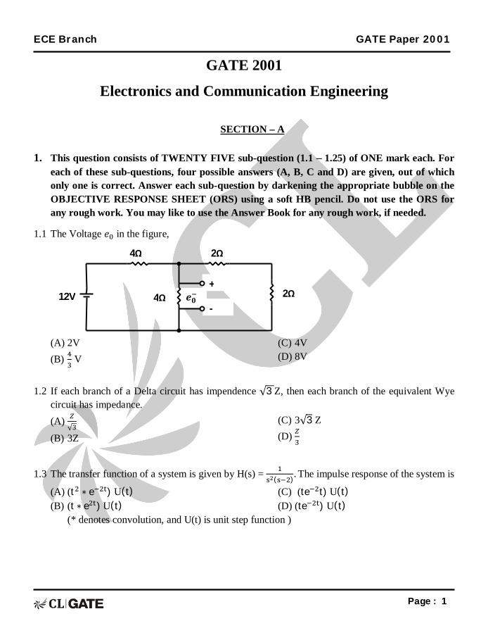
ECE Branch GATE Paper 2001 Page : 1 GATE 2001 Electronics and Communication Engineering SECTION – A 1. This question consists of TWENTY FIVE sub-question (1.1 – 1.25) of ONE mark each. For each of these sub-questions, four possible answers (A, B, C and D) are given, out of which only one is correct. Answer each sub-question by darkening the appropriate bubble on the OBJECTIVE RESPONSE SHEET (ORS) using a soft HB pencil. Do not use the ORS for any rough work. You may like to use the Answer Book for any rough work, if needed. 1.1 The Voltage in the figure, (A) 2V (B) ସ ଷ V (C) 4V (D) 8V 1.2 If each branch of a Delta circuit has impendence √3 Z, then each branch of the equivalent Wye circuit has impedance. (A) √ଷ (B) 3Z (C) 3√3 Z (D) ଷ 1.3 The transfer function of a system is given by H(s) = ଵ ୱ మ (ୱଶ) . The impulse response of the system is (A) (t ଶ ∗ e ଶ୲ ) U(t) (B) (t ∗ e ଶ୲ ) U(t) (C) (te ଶ t) U(t) (D) (te ଶ୲ ) U(t) (* denotes convolution, and U(t) is unit step function ) - + 12V 4Ω 4Ω 2Ω 2Ω
Transcript of GATE 2001 Electronics and Communication...
ECE Branch GATE Paper 2001
Page : 1
GATE 2001
Electronics and Communication Engineering
SECTION – A
1. This question consists of TWENTY FIVE sub-question (1.1 – 1.25) of ONE mark each. For each of these sub-questions, four possible answers (A, B, C and D) are given, out of which only one is correct. Answer each sub-question by darkening the appropriate bubble on the OBJECTIVE RESPONSE SHEET (ORS) using a soft HB pencil. Do not use the ORS for any rough work. You may like to use the Answer Book for any rough work, if needed.
1.1 The Voltage 푒 in the figure,
(A) 2V (B) V
(C) 4V (D) 8V
1.2 If each branch of a Delta circuit has impendence √3 Z, then each branch of the equivalent Wye circuit has impedance. (A)
√
(B) 3Z
(C) 3√3 Z (D)
1.3 The transfer function of a system is given by H(s) = ( ). The impulse response of the system is
(A) (t ∗ e ) U(t) (B) (t ∗ e ) U(t)
(C) (te t) U(t) (D) (te ) U(t)
(* denotes convolution, and U(t) is unit step function )
-
+ 풆ퟎ 12V
4Ω
4Ω
2Ω
2Ω

ECE Branch GATE Paper 2001
Page : 2
1.4 The admittance parameter 푌 in the 2-point network in the figure,
(A) −0.2 mho (B) 0.1 mho
(C) −0.05 mho (D) 0.05 mho
1.5 The region of convergence of the z-transform of a unit step function is
(A) |z| > 1 (B) |z| < 1
(C) (Real part of z) > 0 (D) (Real part of z) < 0
1.6 The current gain of a BJT is
(A) g r
(B)
(C) g rπ
(D) π
1.7 MOSFET can be used as a (A) current controlled capacitor (B) voltage controlled capacitor
(C) current controlled inductor (D) voltage controlled inductor
1.8 The effective channel length of a MOSFET in saturation decreases with increase in
(A) gate voltage (B) drain voltage
(C) source voltage (D) body voltage
1.9 The ideal OP-AMP has the following characteristics.
(A) R = ∞, A = ∞, R = 0 (B) R = 0, A = ∞, R = 0
(C) R = ∞, A = ∞, R = ∞ (D) R = 0, A = ∞, R = ∞
1.10 The 2’s complement representation of −17 is
(A) 01110 (B) 01111
(C) 11110 (D) 10001
20Ω I1 I2
5Ω 10Ω E1↑ ↑E2

ECE Branch GATE Paper 2001
Page : 3
1.11 Consider the following two statements: Statement 1: A stable multivibrator can be used for generating square wave. Statement 2: B stable multivibrator can be used for storing binary information. (A) Only statement 1 is correct (B) Only statement 2 is correct (C) Both the statements 1 and 2 are correct (D) Both the statements 1 and 2 are incorrect.
1.12 For the ring oscillator shown in the figure, the propagation delay of each inverter is 100 pico sec. What is the fundamental frequency of the oscillator output?
(A) 10 MHz (B) 100 MHz
(C) 1 GHz (D) 2 GHz
1.13 An 8085 microprocessor based system uses a 4K × 8 bit RAM whose starting address is AA00 H.
The address of the last byte in this RAM is (A) 0FFF H (B) 1000 H
(C) B9FF H (D) BA00 H
퐕ퟎ
ECE Branch GATE Paper 2001
Page : 4
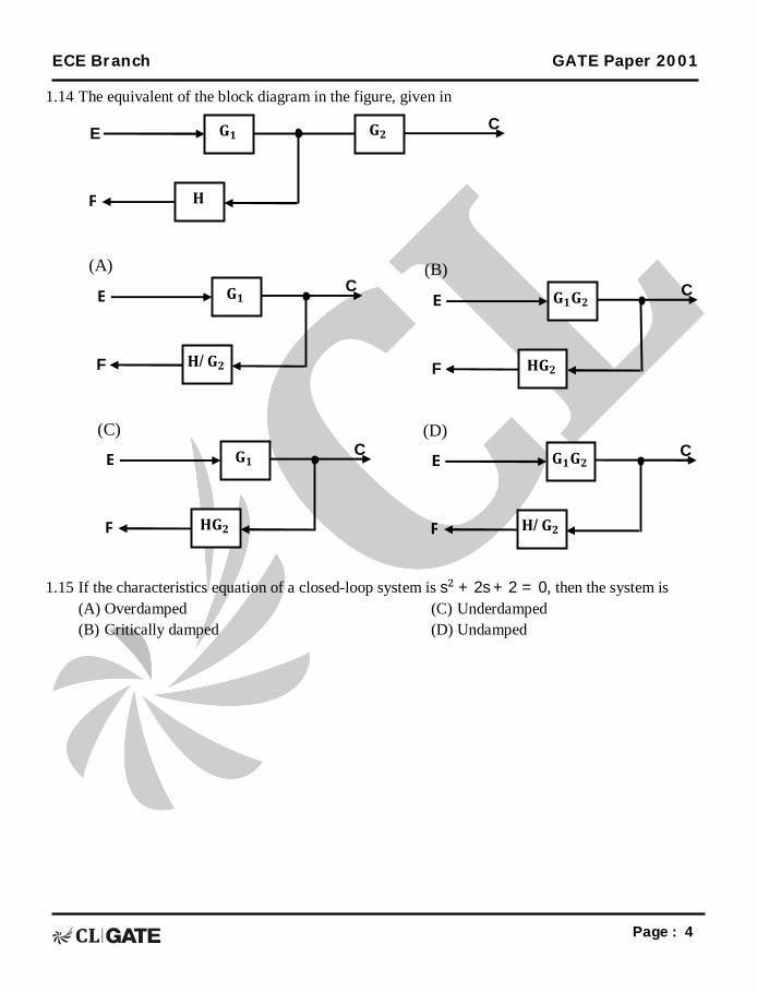
1.14 The equivalent of the block diagram in the figure, given in
1.15 If the characteristics equation of a closed-loop system is s + 2s + 2 = 0, then the system is
(A) Overdamped (B) Critically damped
(C) Underdamped (D) Undamped
퐆ퟏ
퐇/퐆ퟐ
E
F
C (A)
퐆ퟏ퐆ퟐ
퐇퐆ퟐ
E
F
C (B)
퐆ퟏ
퐇퐆ퟐ
E
F
C (C)
퐆ퟏ퐆ퟐ
퐇/퐆ퟐ
E
F
C (D)
퐆ퟏ 퐆ퟐ
퐇
E
F
C

ECE Branch GATE Paper 2001
Page : 5
1.16 The root-locus diagram for a closed-loop feedback system is shown in the figure is. The system is overdamped.
(A) only if 0 ≤ 퐾 ≤ 1 (B) only if 1 < 퐾 < 5
(C) only if 퐾 > 5 (D) if 0 ≤ 퐾 < 1 or 퐾 > 5
1.17 The Nyquist plot for the open-loop transfer function G(s) of a unity negative feedback system is
shown in the figure, if G(s) has no pole in the right-half of s-plane, the number of roots of the system characteristic equation in the right-half of s-plane is
(A) 0 (B) 1
(C) 2 (D) 3
G(s)-plane
퐑퐞(퐬)
퐈퐦(퐬)
−ퟏ
풋흎
흈 풌 = ퟎ
−ퟏ
풌 = ퟏ
−ퟐ −ퟑ
풌 = ퟎ 풌 = ∞
풌 = ퟓ
∞⟵ 풌

ECE Branch GATE Paper 2001
Page : 6
1.18 Let 훿(푡) denote the delta function. The value of the integral ∫ δ(t) cos dt∞∞ is
(A) 1 (B) −1 (C) 0 (D) π
1.19 A bandlimited signal is sampled at the Nyquist rate. The signal can be recovered by passing the samples through (A) an RC filter (B) an envelope detector (C) a PLL (D) an ideal low-pass filter with the appropriate bandwidth.
1.20 The PDF of a Gaussian random variable X is given by 푃푥(푥) =√
푒( )
. The probability of
the event X=4 is (A)
(B) √ π
(C) 0 (D)
1.21 If a signal 푓(푡) has energy E, the energy of the signal 푓(2푡) is equal to (A) E (B) (C) 2E (D) 4E
1.22 A transmission line is distortionless if (A) 푅퐿 = (B) 푅퐿 = 퐺퐶 (C) 퐿퐺 = 푅퐶 (D) 푅퐺 = 퐿퐶
ECE Branch GATE Paper 2001
Page : 7
1.23 If a plane electromagnetic wave satisfies the equation = c , the wave propagates in the (A) 푥 −direction (B) 푧 −direction (C) 푦 −direction (D) 푥푦 plane at an angle of 45 between the 푥 and 푧 directions
1.24 The phase velocity of waves propagating in a hollow metal waveguide is (A) greater than the velocity of light in free space. (B) less than the velocity of light in free space. (C) equal to the velocity of light in free space. (D) equal to the group velocity
1.25 The dominant mode in a rectangular waveguide is TE10, because this mode has (A) no attenuation (B) no cut-off (C) no magnetic field component (D) the higher cut-off wavelength
2. This question consists of TWENTY FIVE sub-questions (2.1 – 2.25) of TWO marks each. For each of these sub-questions, four possible answers (A, B, C and D) are given, out of which only one is correct. Answer each sub-question by darkening the appropriate bubble on the OBJECTIVE RESPONSE SHEET (ORS) using a soft HB pencil. Do not use the ORS for any rough work. You may like to use the Answer Book for any rough work, if needed.
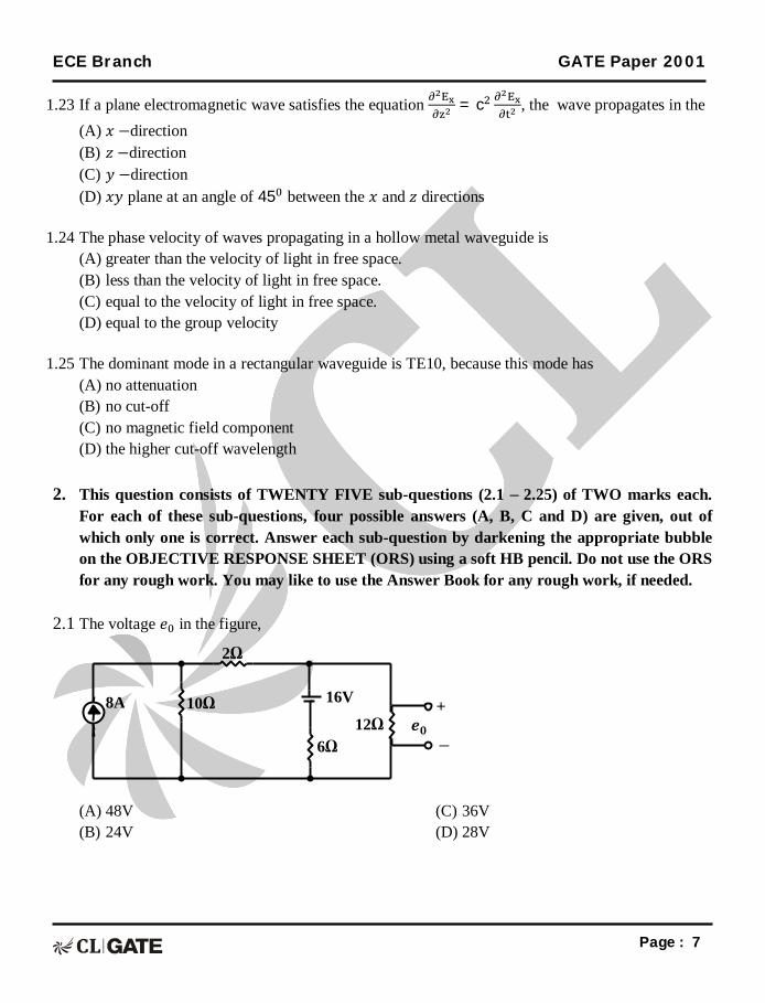
2.1 The voltage 푒 in the figure,
(A) 48V (B) 24V
(C) 36V (D) 28V
−
+ 풆ퟎ 12Ω
6Ω
2Ω
10Ω 16V 8A
ECE Branch GATE Paper 2001
Page : 8
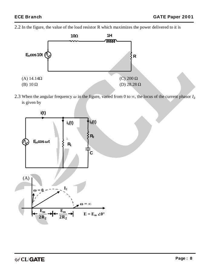
2.2 In the figure, the value of the load resistor R which maximizes the power delivered to it is
(A) 14.14Ω (B) 10 Ω
(C) 200 Ω (D) 28.28 Ω
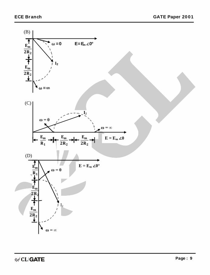
2.3 When the angular frequency 휔 in the figure, varied from 0 to ∞, the locus of the current phasor 퐼
is given by
Emcos 10t R
1H 10Ω
R2
R1
i1(t) i2(t)
i(t)
Emcos 흎t
C
E = Em ∠0°
ω = ∞ 퐄퐦ퟐ퐑ퟐ
퐄퐦ퟐ퐑ퟐ
I2 ω = 0
(A)
ECE Branch GATE Paper 2001
Page : 9
퐄퐦ퟐ퐑ퟐ
퐄퐦ퟐ퐑ퟐ
I2
ω = 0
ω = ∞
E = Em ∠0°
(B)
ω = ∞
퐄퐦ퟐ퐑ퟐ
퐄퐦ퟐ퐑ퟐ
I2 ω = 0
E = Em ∠0 퐄퐦퐑ퟏ
(C)
퐄퐦ퟐ퐑ퟐ
퐄퐦ퟐ퐑ퟐ
I2
ω = 0
ω = ∞
E = Em ∠0° 퐄퐦퐑ퟏ
(D)
ECE Branch GATE Paper 2001
Page : 10
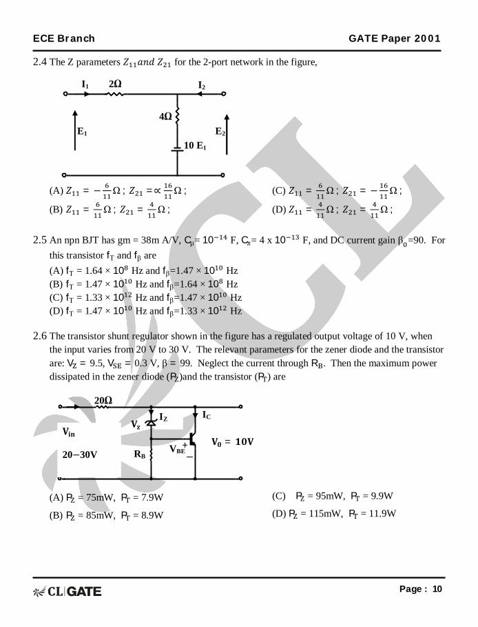
2.4 The Z parameters 푍 푎푛푑 푍 for the 2-port network in the figure,
(A) 푍 = − Ω ; 푍 =∝ Ω ;
(B) 푍 = Ω ; 푍 = Ω ;
(C) 푍 = Ω ; 푍 = − Ω ;
(D) 푍 = Ω ; 푍 = Ω ;
2.5 An npn BJT has gm = 38m A/V, Cµ= 10 F, Cπ= 4 x 10 F, and DC current gain β =90. For this transistor fΤ and fβ are (A) fΤ = 1.64 × 10 Hz and fβ=1.47 × 10 Hz (B) fΤ = 1.47 × 10 Hz and fβ=1.64 × 10 Hz (C) fΤ = 1.33 × 10 Hz and fβ=1.47 × 10 Hz (D) fΤ = 1.47 × 10 Hz and fβ=1.33 × 10 Hz
2.6 The transistor shunt regulator shown in the figure has a regulated output voltage of 10 V, when the input varies from 20 V to 30 V. The relevant parameters for the zener diode and the transistor are: V = 9.5, V = 0.3 V, β = 99. Neglect the current through R . Then the maximum power dissipated in the zener diode (P )and the transistor (P ) are
(A) P = 75mW, P = 7.9W
(B) P = 85mW, P = 8.9W
(C) P = 95mW, P = 9.9W
(D) P = 115mW, P = 11.9W
2Ω
10 E1
4Ω E1 E2
I1 I2
VBE +
IZ 퐕퐳
IC
퐕퐢퐧
20−30V
20Ω
RB − 퐕ퟎ = ퟏퟎ퐕
ECE Branch GATE Paper 2001
Page : 11
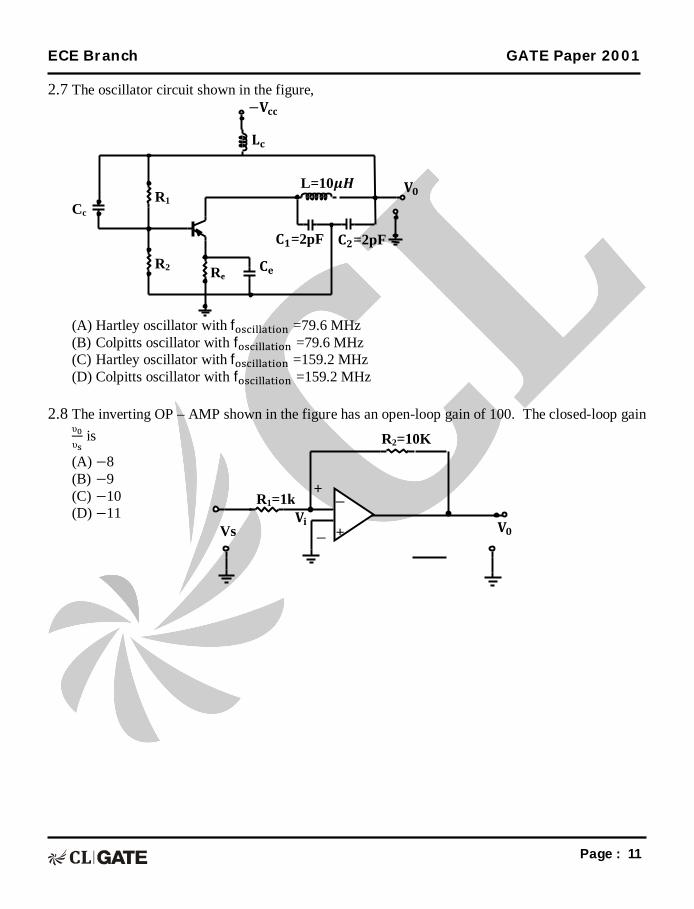
2.7 The oscillator circuit shown in the figure,
(A) Hartley oscillator with f =79.6 MHz (B) Colpitts oscillator with f =79.6 MHz (C) Hartley oscillator with f =159.2 MHz (D) Colpitts oscillator with f =159.2 MHz
2.8 The inverting OP – AMP shown in the figure has an open-loop gain of 100. The closed-loop gain υυ
is
(A) −8 (B) −9 (C) −10 (D) −11
−퐕퐜퐜
퐕ퟎ L=10흁푯
퐋퐜
퐂ퟐ=2pF 퐂ퟏ=2pF
퐂퐞 Re R2
R1 Cc
R1=1k
R2=10K
Vs 퐕ퟎ 퐕퐢
−
+
+
−
ECE Branch GATE Paper 2001
Page : 12
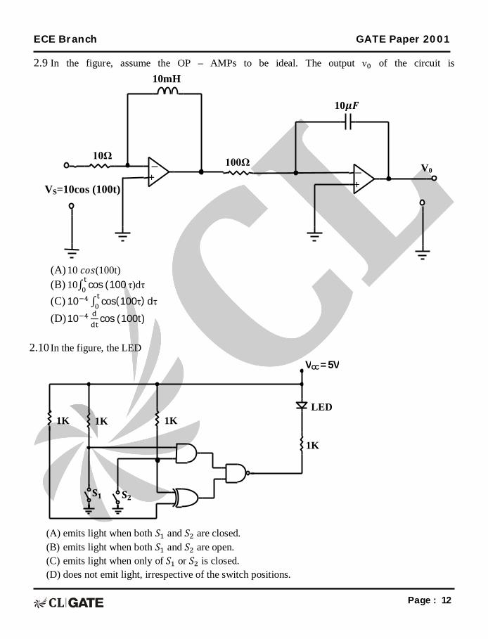
2.9 In the figure, assume the OP – AMPs to be ideal. The output ν of the circuit is
(A) 10 푐표푠(100t) (B) 10∫ cos (100 τ)dτ (C) 10 ∫ cos(100τ) dτ
(D) 10 cos (100t)
2.10 In the figure, the LED
(A) emits light when both 푆 and 푆 are closed. (B) emits light when both 푆 and 푆 are open. (C) emits light when only of 푆 or 푆 is closed. (D) does not emit light, irrespective of the switch positions.
VCC = 5V
LED
퐒ퟐ 퐒ퟏ
1K
1K 1K 1K
10mH
VS=10cos (100t)
100Ω
10흁푭
10Ω V0
+ − −
+
ECE Branch GATE Paper 2001
Page : 13
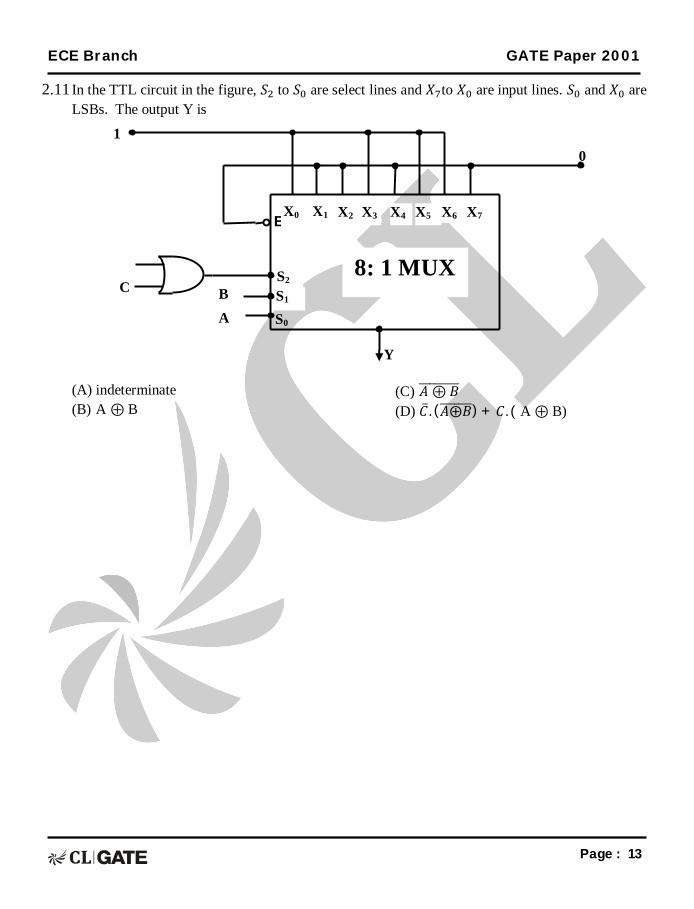
X1 X2 X3 X4 X5 X6 X7 X0
S2
S0 S1
A B
Y
8: 1 MUX
0 1
C
E
2.11 In the TTL circuit in the figure, 푆 to 푆 are select lines and 푋 to 푋 are input lines. 푆 and 푋 are LSBs. The output Y is
(A) indeterminate (B) A ⊕ B
(C) 퐴⊕퐵 (D) 퐶. (퐴⨁퐵) + 퐶. ( A ⊕ B)
ECE Branch GATE Paper 2001
Page : 14
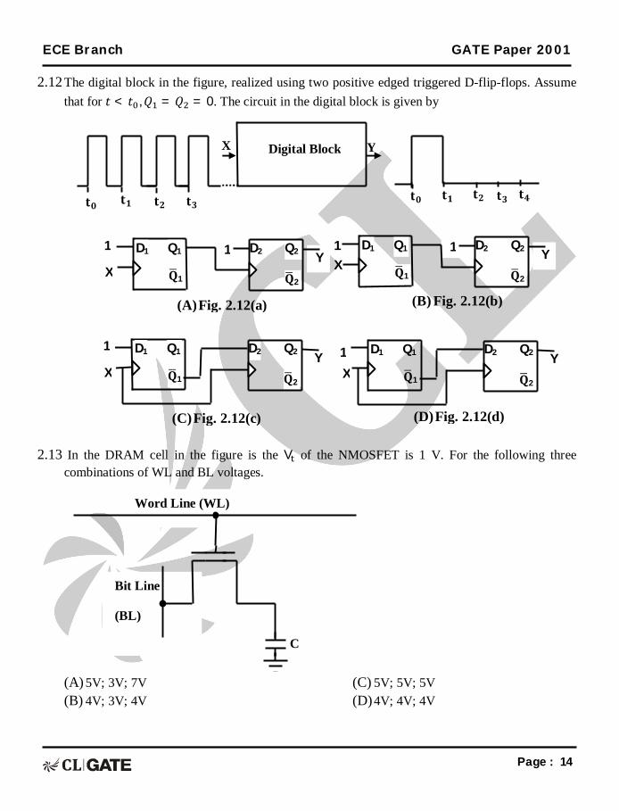
2.12 The digital block in the figure, realized using two positive edged triggered D-flip-flops. Assume that for 푡 < 푡 ,푄 = 푄 = 0. The circuit in the digital block is given by
2.13 In the DRAM cell in the figure is the V of the NMOSFET is 1 V. For the following three
combinations of WL and BL voltages.
(A) 5V; 3V; 7V (B) 4V; 3V; 4V
(C) 5V; 5V; 5V (D) 4V; 4V; 4V
퐭ퟎ
X Y Digital Block
퐭ퟏ 퐭ퟐ 퐭ퟑ 퐭ퟎ 퐭ퟏ 퐭ퟐ 퐭ퟑ 퐭ퟒ
C
Bit Line
(BL)
Word Line (WL)
Y 1
퐐2
Q2 D2D1 Q1
퐐1
1 1
X Y
1
퐐2
Q2 D2D1 Q1
퐐1
Y
퐐2
Q2 D2D1 Q1
퐐1
1 1
X Y
퐐2
Q2 D2D1 Q1
퐐1
1
X
1
X
(A) Fig. 2.12(a) (B) Fig. 2.12(b)
(C) Fig. 2.12(c) (D) Fig. 2.12(d)
ECE Branch GATE Paper 2001
Page : 15
2.14 The impulse response functions of four linear systems S , S , S , S are given respectively by ℎ (푡) = 1 ℎ (푡) = 푈(푡)
ℎ (푡) = ( ) ℎ (푡) = 푒 푈(푡) Where 푈(푡) is the unit step function. Which of these systems is time invariant, causal, and stable? (A) S (B) S
(C) S (D) S
2.15 An electrical system and its signal-flow graph representations are shown in the figure
respectively. The values of G and H, respectively, are
(A) ( )
( ) ( ) ( ), ( )
( ) ( )
(B) ( )( ) ( ) ( )
, ( )( ) ( )
(C) ( )( ) ( ) ( )
, ( )( ) ( )
(D) ( )( ) ( ) ( )
, ( )( ) ( )
2.16 The open-loop DC gain of a unity negative feedback system with closed-loop transfer function
is
(A) (C) 4
(B) (D) 13
퐙ퟏ(퐒) 퐙ퟐ(퐒)
퐙ퟒ(퐒) 퐙ퟑ(퐒) 퐈ퟏ(퐒) 퐈ퟐ(퐒) 퐕퐢(퐒)
퐕ퟎ(퐒)
Fig. 2.15(a)
퐕퐢(퐒) 퐕ퟎ(퐒) H
퐆ퟏ 퐈ퟏ(퐒) 퐈ퟐ(퐒) 퐆ퟐ 퐆ퟑ
Fig. 2.15(b)
ECE Branch GATE Paper 2001
Page : 16
2.17 The feedback control system in the figure is stable.
(A) for all 퐾 ≥ 0 (B) only if 퐾 ≥ 1 (C) only if 0 ≤ 퐾 < 1 (D) only if 0 ≤ 퐾 ≤ 1
2.18 A video transmission system transmits 625 picture frames per second. Each frame consists of a 400 × 400 pixel grid with 64 intensity levels per pixel. The data rate of the system is (A) 16 Mbps (B) 100 Mbps
(C) 600 Mbps (D) 6.4 Gbps
2.19 The Nyquist sampling interval, for the signal 푆푖푛 푐(700푡) + 푆푖푛 푐(500푡) is
(A) sec
(B) sec
(C) sec
(D) sec
2.20 During transmission over a communication channel, bit errors occur independently with probability 푝. If a block of 푛 bits is transmitted, the probability of at most one bit error is equal to (A) 1−(1-p)n
(B) p+(n−1)(1−p) (C) np(1−p)n-1 (D) (1−p)n+ np(1−p)n-1
2.21 The PSD and the power of a signal g(t) are, respectively, Sg(휔) and Pg. The PSD and the power of the signal ag(t) are, respectively, (A) a2푆 (휔) and 푎 푃 (B) 푎 푆 (휔) and 푎푃 (C) 푎푆 (휔) and 푎 푃 (D) 푎푆 (휔) and 푎푃
푲 ≥ ퟎ 푺 − ퟐ(푺 + ퟐ)ퟐ
푹(풔) 푪(풔) +
−
푺 − ퟐ

ECE Branch GATE Paper 2001
Page : 17
2.22 A material has conductivity of 10 mho/m and a relative permittivity of 4. The frequency at which the conduction current in the medium is equal to the displacement current is (A) 45MHz (B) 90 MHz
(C) 450 MHz (D) 900 MHz
2.23 A uniform plane electromagnetic wave incident normally on a plane surface of a dielectric
material is reflected with a VSWR of 3. What is the percentage of incident power that is reflected? (A) 10% (B) 25%
(C) 50% (D) 75%
2.24 A medium wave radio transmitter operating at a wavelength of 492 m has a tower antenna of
height 124 m. What is the radiation resistance of the antenna? (A) 25 Ω (B) 36.5 Ω
(C) 50 Ω (D) 73 Ω
2.25 In a uniform linear array, four isotropic radiating elements are spaced apart. The progressive phase shift between the elements required for forming the main beam at 60o off the end-fire is (A) –π radians (B) − π radians
(C) − π radians
(D) − π radians
SECTION – B (75 Marks)
This section consists of TWENTY questions of FIVE marks each. ANY FIFTEEN out of these questions have to be answered in the Answer Book provided. 3. For the circuit shown in the figure, determine the phasors E , E , I, and I .
~
풋ퟐΩ
퐈ퟏ
ퟎ.ퟓΩ 퐄ퟎ
ퟎ.ퟓΩ 퐄ퟐ 풋Ω 푰
퐄ퟏ = ퟏퟎ∠ퟐퟎퟎ
ퟏΩ
−풋Ω
ECE Branch GATE Paper 2001
Page : 18
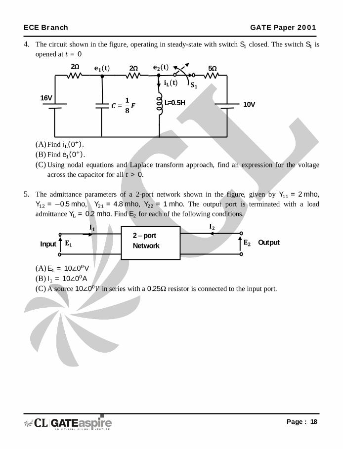
4. The circuit shown in the figure, operating in steady-state with switch S closed. The switch S is opened at 푡 = 0
(A) Find i (0 ). (B) Find e (0 ). (C) Using nodal equations and Laplace transform approach, find an expression for the voltage
across the capacitor for all 푡 > 0.
5. The admittance parameters of a 2-port network shown in the figure, given by Y = 2 mho, Y = −0.5 mho, Y = 4.8 mho, Y = 1 mho. The output port is terminated with a load admittance Y = 0.2 mho. Find E for each of the following conditions.
(A) E = 10∠0 V (B) I = 10∠0 A (C) A source 10∠0 푉 in series with a 0.25Ω resistor is connected to the input port.
2 – port Network
퐈ퟏ 퐈ퟐ
퐄ퟏ Input 퐄ퟐ Output
10V L=0.5H
퐢퐋(퐭)
2Ω 퐞ퟏ(퐭) 2Ω 퐞ퟐ(퐭)
16V 푪 =
ퟏퟖ푭
퐒ퟏ
5Ω
ECE Branch GATE Paper 2001
Page : 19
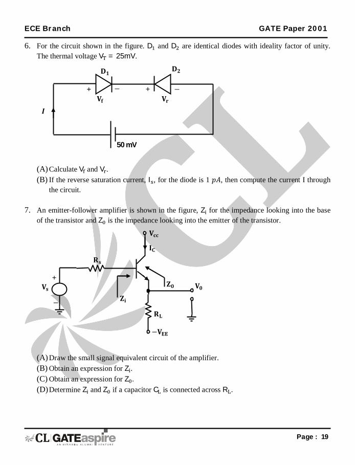
6. For the circuit shown in the figure. D and D are identical diodes with ideality factor of unity. The thermal voltage V = 25mV.
(A) Calculate V and V . (B) If the reverse saturation current, I , for the diode is 1 푝퐴, then compute the current I through
the circuit.
7. An emitter-follower amplifier is shown in the figure, Z for the impedance looking into the base of the transistor and Z is the impedance looking into the emitter of the transistor.
(A) Draw the small signal equivalent circuit of the amplifier. (B) Obtain an expression for Z . (C) Obtain an expression for Z . (D) Determine Z and Z if a capacitor C is connected across R .
+
−
퐕퐬
퐑퐬
퐕ퟎ
퐑퐋
−퐕퐄퐄
퐙ퟎ
퐙퐢
퐈퐂
퐕퐜퐜
퐃ퟐ 퐃ퟏ
퐕퐫 퐕퐟
50 mV
푰
+ − + −
ECE Branch GATE Paper 2001
Page : 20
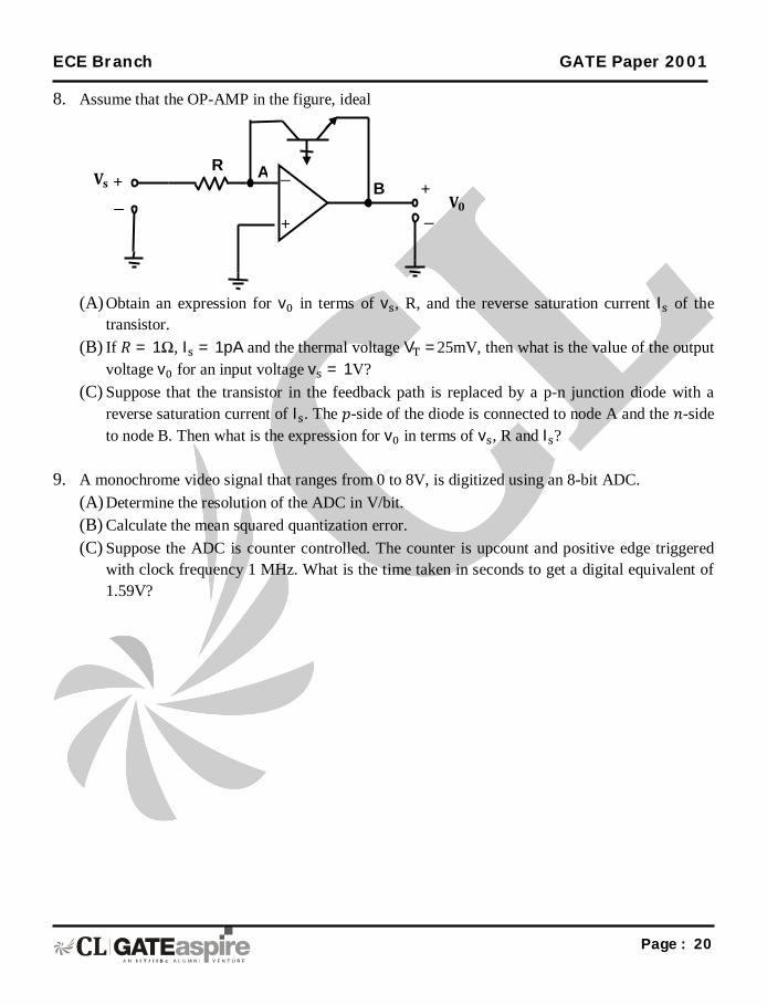
8. Assume that the OP-AMP in the figure, ideal
(A) Obtain an expression for v in terms of v , R, and the reverse saturation current I of the
transistor. (B) If 푅 = 1Ω, I = 1pA and the thermal voltage V =25mV, then what is the value of the output
voltage v for an input voltage v = 1V? (C) Suppose that the transistor in the feedback path is replaced by a p-n junction diode with a
reverse saturation current of I . The 푝-side of the diode is connected to node A and the 푛-side to node B. Then what is the expression for v in terms of v , R and I ?
9. A monochrome video signal that ranges from 0 to 8V, is digitized using an 8-bit ADC.
(A) Determine the resolution of the ADC in V/bit. (B) Calculate the mean squared quantization error. (C) Suppose the ADC is counter controlled. The counter is upcount and positive edge triggered
with clock frequency 1 MHz. What is the time taken in seconds to get a digital equivalent of 1.59V?
−
+
B 퐕ퟎ
+
−
A R 퐕퐬 +
−
ECE Branch GATE Paper 2001
Page : 21
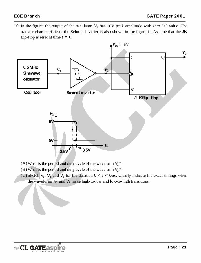
10. In the figure, the output of the oscillator, V has 10V peak amplitude with zero DC value. The transfer characteristic of the Schmitt inverter is also shown in the figure is. Assume that the JK flip-flop is reset at time 푡 = 0.
(A) What is the period and duty cycle of the waveform V ? (B) What is the period and duty cycle of the waveform V ? (C) Sketch V , V and V for the duration 0 ≤ 푡 ≤ 6휇푠. Clearly indicate the exact timings when
the waveforms V and V make high-to-low and low-to-high transitions.
퐕ퟑ
퐕퐜퐜 = ퟓ퐕
0.5 MHz Sinewave oscillator
Q J
K
퐕ퟐ 퐕ퟏ
Oscillator Schmitt inverter J−K flip−flop
퐕ퟏ 3.5V 2.5V
0V
5V
퐕ퟐ
ECE Branch GATE Paper 2001
Page : 22
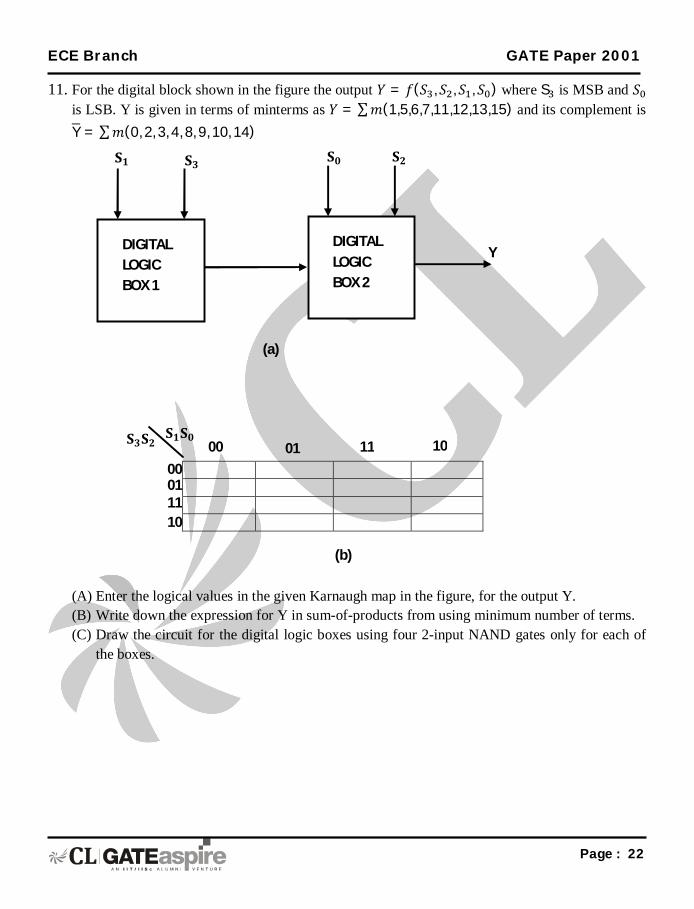
11. For the digital block shown in the figure the output 푌 = 푓(푆 , 푆 , 푆 , 푆 ) where S is MSB and 푆 is LSB. Y is given in terms of minterms as 푌 = ∑푚(1,5,6,7,11,12,13,15) and its complement is Y = ∑푚(0, 2, 3, 4, 8, 9, 10, 14)
(A) Enter the logical values in the given Karnaugh map in the figure, for the output Y. (B) Write down the expression for Y in sum-of-products from using minimum number of terms. (C) Draw the circuit for the digital logic boxes using four 2-input NAND gates only for each of
the boxes.
00 01 11 10
00 01 11 10
(b)
퐒ퟏ퐒ퟎ
퐒ퟑ퐒ퟐ
DIGITAL LOGIC BOX 1
DIGITAL LOGIC BOX 2
퐒ퟏ 퐒ퟐ 퐒ퟎ 퐒ퟑ
(a)
Y

ECE Branch GATE Paper 2001
Page : 23
12. Consider the following sequence of instructions for an 8085 microprocessor based system. Memory Address Instructions FF00 MVI A, FFH FF02 INR A FF03 JC FF0C H FF06 ORI A8H FF08 JM FF15 H FF0B XRA A FF0C OUT PORT 1 FF0E HLT FF10 XRI FF H FF12 OUT PORT2 FF14 HLT FF15 MVI A, FF H FF17 ADI 02 H FF19 RAL FF1A JZ FF23 H FF1D JC FF10 H FF20 JNC FF12 H FF23 CMA FF24 OUT PORT3 FF26 HLT (A) If the program execution begins at the location FF00 H, write down the sequence of
instructions which are actually executed till a HLT instruction. (Assume all flags are initially RESET).
(B) Which of the three ports (PORT1, PORT2 and PORT3) will be loaded with data, and what is the bit pattern of the data?
ECE Branch GATE Paper 2001
Page : 24
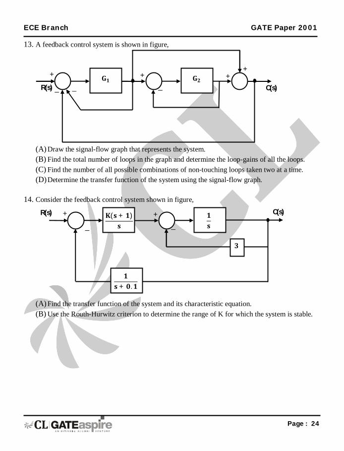
13. A feedback control system is shown in figure,
(A) Draw the signal-flow graph that represents the system. (B) Find the total number of loops in the graph and determine the loop-gains of all the loops. (C) Find the number of all possible combinations of non-touching loops taken two at a time. (D) Determine the transfer function of the system using the signal-flow graph.
14. Consider the feedback control system shown in figure,
(A) Find the transfer function of the system and its characteristic equation. (B) Use the Routh-Hurwitz criterion to determine the range of K for which the system is stable.
퐊(퐬 + ퟏ)퐬
R(s) C(s) +
− −
+ ퟏ퐬
ퟑ
ퟏ퐬 + ퟎ.ퟏ
퐆ퟏ 퐆ퟐ R(s) C(s)
+
− − −
+ + +
ECE Branch GATE Paper 2001
Page : 25
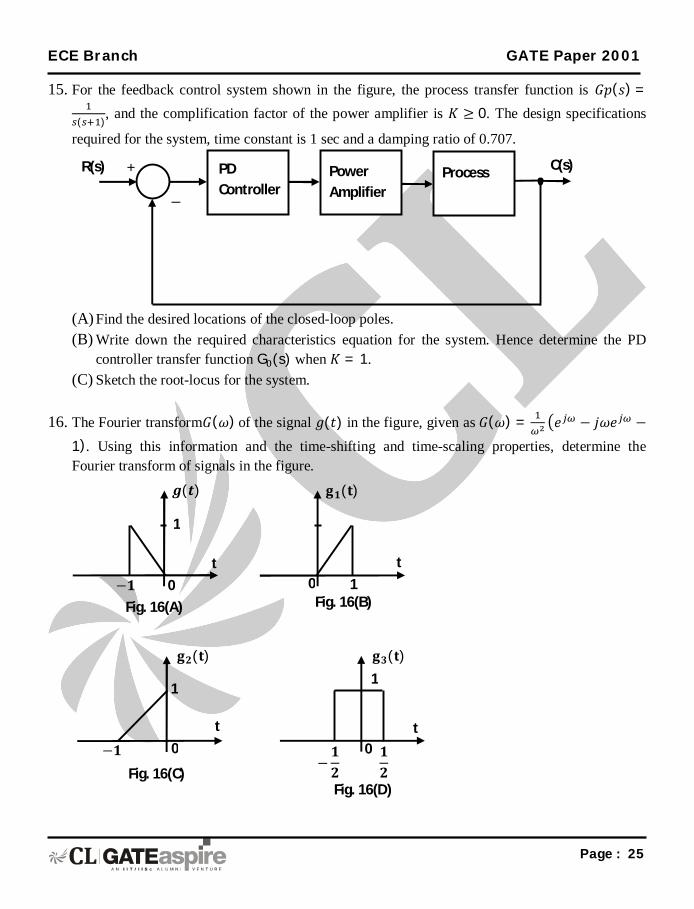
15. For the feedback control system shown in the figure, the process transfer function is 퐺푝(푠) =
( ), and the complification factor of the power amplifier is 퐾 ≥ 0. The design specifications
required for the system, time constant is 1 sec and a damping ratio of 0.707.
(A) Find the desired locations of the closed-loop poles. (B) Write down the required characteristics equation for the system. Hence determine the PD
controller transfer function G (s) when 퐾 = 1. (C) Sketch the root-locus for the system.
16. The Fourier transform퐺(휔) of the signal 푔(푡) in the figure, given as 퐺(휔) = 푒 − 푗휔푒 −1). Using this information and the time-shifting and time-scaling properties, determine the Fourier transform of signals in the figure.
1
−ퟏ 0 0 1
t
1
−ퟏ 0 −ퟏퟐ
ퟏퟐ
0
t t
t
퐠ퟐ(퐭)
품(풕) 퐠ퟏ(퐭)
퐠ퟑ(퐭)
Fig. 16(A) Fig. 16(B)
Fig. 16(C) Fig. 16(D)
1
R(s) C(s) +
−
PD Controller
Power Amplifier
Process
ECE Branch GATE Paper 2001
Page : 26
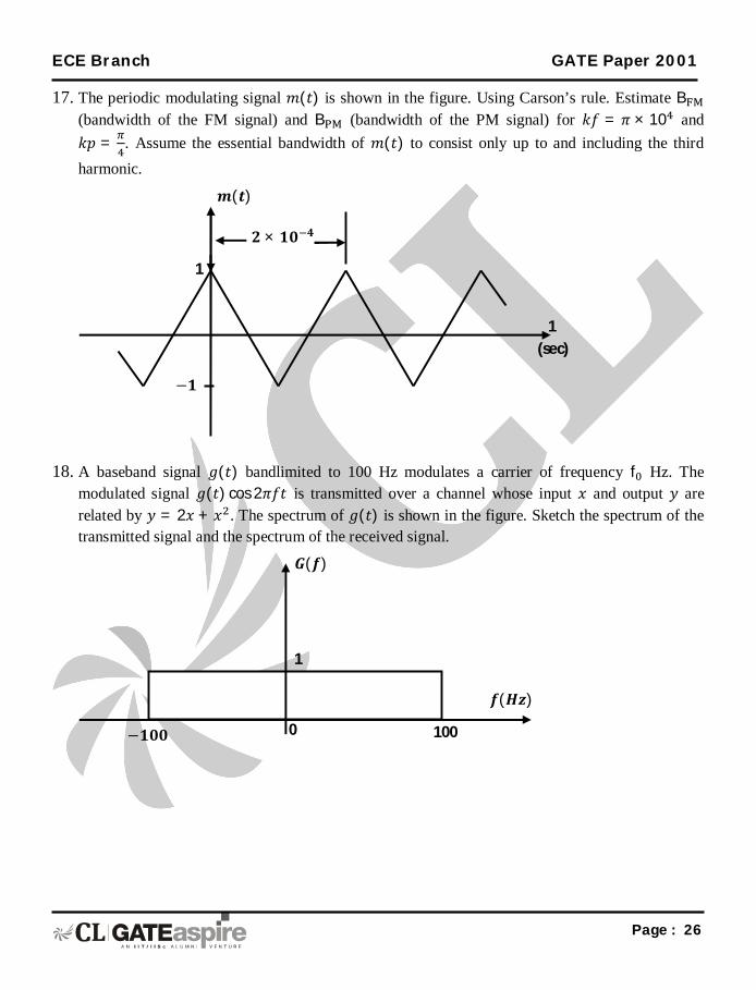
17. The periodic modulating signal 푚(푡) is shown in the figure. Using Carson’s rule. Estimate B (bandwidth of the FM signal) and B (bandwidth of the PM signal) for 푘푓 = 휋 × 10 and 푘푝 = . Assume the essential bandwidth of 푚(푡) to consist only up to and including the third harmonic.
18. A baseband signal 푔(푡) bandlimited to 100 Hz modulates a carrier of frequency f Hz. The modulated signal 푔(푡) cos 2휋푓푡 is transmitted over a channel whose input 푥 and output 푦 are related by 푦 = 2푥 + 푥 . The spectrum of 푔(푡) is shown in the figure. Sketch the spectrum of the transmitted signal and the spectrum of the received signal.
푮(풇)
1
−ퟏퟎퟎ 0 100
풇(푯풛)
풎(풕)
ퟐ× ퟏퟎ ퟒ
1
−ퟏ
1 (sec)

ECE Branch GATE Paper 2001
Page : 27
19. A periodic signal 푔(푡) is shown in the figure. Determine the PSD of 푔(푡).
20. A system of three electric charges lying in a straight line is in equilibrium. Two of the charges are
positive with magnitudes Q and 2Q, and are 50cm apart. Determine the sign, magnitude and position of the third charge.
21. A medium has a breakdown strength of 16 KV/m r.m.s. its relative permeability is 1.0 and relative permittivity is 4.0 A plane electromagnetic wave is transmitted through the medium. Calculate the maximum possible power flow density and the associated magnetic field.
22. A rectangular hollow metal waveguide has dimensions 푎 = 2.29cm and 푏 = 1.02cm. Microwave power at 10 GHz is transmitted through the waveguide in the TE mode. (A) Calculate the cut-off wavelength and the guide wavelength for this mode. (B) What are the other (TE or TM) modes that can propagate through the waveguide? (C) If 푎 = 푏 = 2.29cm, what are the modes which can propagate through the waveguide?
−ퟐ흅 −흅ퟐ
훑ퟐ
ퟐ흅 ퟒ흅
t sec
Fig. 19
1
품(풕)


![GATE 2021 [Afternoon Session] 1 Electronics ...](https://static.fdocument.org/doc/165x107/61f934f172f3ef648a782147/gate-2021-afternoon-session-1-electronics-.jpg)