EVAL-AD7176-2SDZ User Guide - Analog Devices · 2. Connect the EVAL -SDP-CB1Z evaluation board to...
40
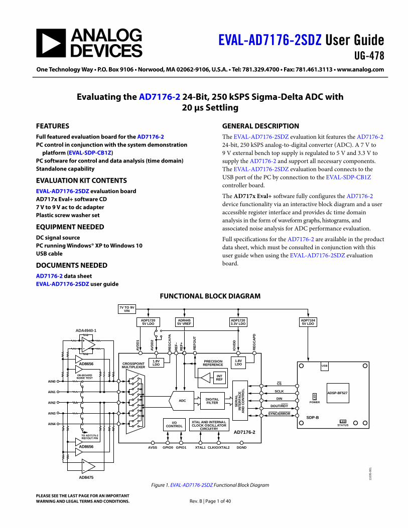
EVAL-AD7176-2SDZ User Guide UG-478 One Technology Way • P.O. Box 9106 • Norwood, MA 02062-9106, U.S.A. • Tel: 781.329.4700 • Fax: 781.461.3113 • www.analog.com Evaluating the AD7176-2 24-Bit, 250 kSPS Sigma-Delta ADC with 20 μs Settling PLEASE SEE THE LAST PAGE FOR AN IMPORTANT WARNING AND LEGAL TERMS AND CONDITIONS. Rev. B | Page 1 of 40 FEATURES Full featured evaluation board for the AD7176-2 PC control in conjunction with the system demonstration platform (EVAL-SDP-CB1Z) PC software for control and data analysis (time domain) Standalone capability EVALUATION KIT CONTENTS EVAL-AD7176-2SDZ evaluation board AD717x Eval+ software CD 7 V to 9 V ac to dc adapter Plastic screw washer set EQUIPMENT NEEDED DC signal source PC running Windows® XP to Windows 10 USB cable DOCUMENTS NEEDED AD7176-2 data sheet EVAL-AD7176-2SDZ user guide GENERAL DESCRIPTION The EVAL-AD7176-2SDZ evaluation kit features the AD7176-2 24-bit, 250 kSPS analog-to-digital converter (ADC). A 7 V to 9 V external bench top supply is regulated to 5 V and 3.3 V to supply the AD7176-2 and support all necessary components. The EVAL-AD7176-2SDZ evaluation board connects to the USB port of the PC by connection to the EVAL-SDP-CB1Z controller board. The AD717x Eval+ software fully configures the AD7176-2 device functionality via an interactive block diagram and a user accessible register interface and provides dc time domain analysis in the form of waveform graphs, histograms, and associated noise analysis for ADC performance evaluation. Full specifications for the AD7176-2 are available in the product data sheet, which must be consulted in conjunction with this user guide when using the EVAL-AD7176-2SDZ evaluation board. FUNCTIONAL BLOCK DIAGRAM 11035-001 AVDD1 AVSS GPIO0 GPIO1 XTAL1 CLKIO/XTAL2 DGND REF– REF+ REFOUT AVDD2 REGCAPA AIN0 AIN1 AIN2 AIN3 AIN4 1.8V LDO 1.8V LDO INT REF CROSSPOINT MULTIPLEXER IOVDD REGCAPD I/O CONTROL SERIAL INTERFACE AND CONTROL DIGITAL FILTER AD7176-2 PRECISION REFERENCE XTAL AND INTERNA L CLOCK OSCILLATOR CIRCUITRY SCLK DIN CS DOUT/RDY SYNC/ERROR TO AD7175-2 REFOUT PIN POWER LED STATUS LED ADSP-BF527 USB SDP-B ADC ADP1720 5V LDO ADR445 5V VREF 7V TO 9V VIN ADP1720 3.3V LDO ADP7104 5V LDO ON-BOARD NOISE TEST AD8656 ADA4940-1 AD8656 AD8475 Figure 1. EVAL-AD7176-2SDZ Functional Block Diagram
Transcript of EVAL-AD7176-2SDZ User Guide - Analog Devices · 2. Connect the EVAL -SDP-CB1Z evaluation board to...
EVAL-AD7176-2SDZ User GuideUG-478
One Technology Way • P.O. Box 9106 • Norwood, MA 02062-9106, U.S.A. • Tel: 781.329.4700 • Fax: 781.461.3113 • www.analog.com
Evaluating the AD7176-2 24-Bit, 250 kSPS Sigma-Delta ADC with
20 μs Settling
PLEASE SEE THE LAST PAGE FOR AN IMPORTANT WARNING AND LEGAL TERMS AND CONDITIONS. Rev. B | Page 1 of 40
FEATURES Full featured evaluation board for the AD7176-2 PC control in conjunction with the system demonstration
platform (EVAL-SDP-CB1Z) PC software for control and data analysis (time domain) Standalone capability
EVALUATION KIT CONTENTS EVAL-AD7176-2SDZ evaluation board AD717x Eval+ software CD 7 V to 9 V ac to dc adapter Plastic screw washer set
EQUIPMENT NEEDED DC signal source PC running Windows® XP to Windows 10 USB cable
DOCUMENTS NEEDED AD7176-2 data sheet EVAL-AD7176-2SDZ user guide
GENERAL DESCRIPTION The EVAL-AD7176-2SDZ evaluation kit features the AD7176-2 24-bit, 250 kSPS analog-to-digital converter (ADC). A 7 V to 9 V external bench top supply is regulated to 5 V and 3.3 V to supply the AD7176-2 and support all necessary components. The EVAL-AD7176-2SDZ evaluation board connects to the USB port of the PC by connection to the EVAL-SDP-CB1Z controller board.
The AD717x Eval+ software fully configures the AD7176-2 device functionality via an interactive block diagram and a user accessible register interface and provides dc time domain analysis in the form of waveform graphs, histograms, and associated noise analysis for ADC performance evaluation.
Full specifications for the AD7176-2 are available in the product data sheet, which must be consulted in conjunction with this user guide when using the EVAL-AD7176-2SDZ evaluation board.
FUNCTIONAL BLOCK DIAGRAM
1103
5-00
1
AVDD
1
AVSS GPIO0 GPIO1 XTAL1 CLKIO/XTAL2 DGND
REF–
REF+
REFO
UT
AVDD
2
REG
CAPA
AIN0
AIN1
AIN2
AIN3
AIN4
1.8VLDO
1.8VLDO
INTREF
CROSSPOINTMULTIPLEXER
IOVD
D
REG
CAP
D
I/OCONTROL
SERI
AL
INTE
RFA
CEA
ND C
ON
TRO
L
DIGITALFILTER
AD7176-2
PRECISIONREFERENCE
XTAL AND INTERNALCLOCK OSCILLATOR
CIRCUITRY
SCLK
DIN
CS
DOUT/RDY
SYNC/ERROR
TO AD7175-2REFOUT PIN
POWER
LEDSTATUS
LED
ADSP-BF527
USB
SDP-B
ADC
ADP17205V LDO
ADR4455V VREF
7V TO 9VVIN
ADP17203.3V LDO
ADP71045V LDO
ON-BOARDNOISE TEST
AD8656
ADA4940-1
AD8656
AD8475 Figure 1. EVAL-AD7176-2SDZ Functional Block Diagram
UG-478 EVAL-AD7176-2SDZ User Guide
Rev. B | Page 2 of 40
TABLE OF CONTENTS Features .............................................................................................. 1 Evaluation Kit Contents ................................................................... 1 Equipment Needed ........................................................................... 1 Documents Needed .......................................................................... 1 General Description ......................................................................... 1 Functional Block Diagram .............................................................. 1 Revision History ............................................................................... 2 EVAL-AD7176-2SDZ Quick Start Guide ...................................... 4 Evaluation Board Hardware ............................................................ 5
Device Description ....................................................................... 5 Hardware Link Options ............................................................... 5 Sockets and On-Board Connectors ........................................... 6 Power Supplies .............................................................................. 7 Serial Interface .............................................................................. 7 Analog Inputs ................................................................................ 7 Reference Options ........................................................................ 8 Using the On-Board Amplifiers ................................................. 8
Evaluation Board Software ............................................................ 12
Software Installation .................................................................. 12 Warning ....................................................................................... 12 Installing the AD717X Eval+ Software .................................... 12 Installing the Eval+ Dependencies ........................................... 13 Installing .NET Framework 3.5 on Windows 8/Windows 10 ... 13 Setting Up the System for Data Capture ................................. 14 Launching the Software ............................................................. 14
Evaluation Board Software Operation ......................................... 15 Overview of the Main Window ................................................ 15 Waveform Tab (18) ..................................................................... 17 Histogram Tab (28) .................................................................... 18 Modelled Performance Tab (31)............................................... 19 Registers Tab (45) ....................................................................... 22 Exiting the Software ................................................................... 22
Evaluation Board Schematics and Artwork ................................ 23 Ordering Information .................................................................... 32
Bill of Materials ........................................................................... 32
REVISION HISTORY 4/2018—Rev. A to Rev. B Changed AD7176-2 Eval Board to AD717x Eval+ ... Throughout Changes to Title, Equipment Needed Section, and General Description Section .......................................................................... 1 Deleted Online Resources Section ................................................. 1 Added Evaluation Kit Contents Section and Documents Needed Section ................................................................................. 1 Changes to EVAL-AD7176-2SDZ Quick Start Guide Section ... 4 Changes to Table 1 ............................................................................ 5 Changed On-Board Connectors Section to Sockets and On-Board Connectors Section ............................................................... 6 Changes to Sockets and On-Board Connectors Section ............. 6 Changes to Table 2 ............................................................................ 6 Changes to Serial Interface Section ................................................ 7 Deleted Sockets/Connectors Section and Table 4; Renumbered Sequentially ....................................................................................... 7 Changes to Reference Options Section .......................................... 8 Deleted Figure 3 and Figure 4; Renumbered Sequentially .......... 8 Changes to Figure 4 .......................................................................... 9 Changes to Table 4 ............................................................................ 9 Changes to Figure 5 ........................................................................ 10 Deleted Evaluation Board Setup Procedures Section, Warning Section, and Configuring the Evaluation and SDP Boards Section .............................................................................................. 11 Changed Software Installation Procedures Section to Software Installation Section ......................................................................... 12 Changes to Software Installation Section, Warning Section, Figure 6 Caption, Figure 7, Figure 8, and Figure 9 ..................... 12
Changed Installing the EVAL-SDP-CB1Z System Demonstration Platform Board Drivers Section to Installing the Eval+ Dependencies Section .................................................................... 13 Changes to Figure 10, Installing the Eval+ Dependencies Section, Figure 11, and Figure 12 ................................................. 13 Added Installing .NET Framework 3.5 on Windows 8/Windows 10 Section and Figure 14; Renumbered Sequentially ................ 13 Added Figure 16 and Figure 18 .................................................... 14 Changes to Figure 17 ...................................................................... 14 Changed Software Operation Section to Evaluation Board Software Operation Section .......................................................... 15 Changes to Overview of the Main Window Section ................. 15 Added Figure 19, Configuration Tab (1) Section, Select Product/Evaluation Mode (2) Section, Tutorial Button (3) Section, Functional Block Diagram (4) Section, Configuration Pop-Up Button (5) Section, and Analog and Digital Supply Voltages (6, 7, and 14) Section ...................................................... 15 Deleted ADC Setup Button Section, Start Sampling Button Section, Data Graph Section, Analysis Graph Section, CRC Error Indicator Section, and Figure 20 ........................................ 16 Added Figure 20, External Reference (Ext. REF−(V) and Ext. REF+(V)) (8) Section, Register Configuration Summary (9) Section, Reset ADC (10) Section, Menu Bar (11) Section, File Section, Save Section, Load Section, Exit Section, and Edit Section .............................................................................................. 16 Deleted Noise Test—Quick Start Demonstration Section and Figure 21 .......................................................................................... 17
EVAL-AD7176-2SDZ User Guide UG-478
Rev. B | Page 3 of 40
Added Help Section, Status Bar (12) Section, Device Error (13) Section, External MCLK Frequency (15) Section, Analog Input Voltage (16) Section, External SCLK Frequency (17) Section, Waveform Tab (18) Section, Sampling Mode (19) Section, Samples (20) Section, and Sample (21) Section..........................17 Deleted Reading Samples from the ADC Section and Figure 22........................................................................................18 Added Figure 21, Waveform Graph and Controls (22 and 23) Section, Channel Selection (24) Section, Noise Analysis (25) Section, Analysis Channel (26) Section, Display Units and Axis Controls (27) Section, Histogram Tab (28) Section, and Histogram Graph and Controls Section .....................................18 Deleted DC Waveform Capture Section, DC Testing—Histogram Section, and Figure 23 ...............................................19 Added Figure 22, Figure 23, Modelled Performance Tab (31) Section, and Analysis Channel (32) Section ...............................19 Deleted Save File Section and Figure 24 .....................................20 Added Filter Profile (33) Section, Filter Profile Graph (34) Section, Filter Rejection (35) Section, Filter Performance (36) Section, Figure 24, Filter Step Response (37) Section, Step Response Graph (38) Section, Step Configuration (39) Section, Step Response (40) Section, and Graph Units (41) Section.......20
Added Figure 25, Timing Power / Power (42) Section, Estimated Power Consumption (43) Section, and Timing Diagram (44) Section ...................................................................21 Added Figure 26, Registers Tab (45) Section, Register Tree (46) Section, Register (47) Section, Bitfields (48) Section, Documen-tation (49) Section, and Save (50) and Load (51) Section .........22 Changes to Exiting the Software Section ....................................22 Changes to Figure 27 ....................................................................23 Changes to Figure 28 ....................................................................24 Changes to Figure 29 ....................................................................25 Changes to Figure 31 ....................................................................27 Added Ordering Information Section.........................................32 Changes to Bill of Materials Section............................................32 Changes to Table 7 ........................................................................32 4/2014—Rev. 0 to Rev. A Changes to the Reference Options Section...................................8 11/2012—Revision 0: Initial Version
UG-478 EVAL-AD7176-2SDZ User Guide
Rev. B | Page 4 of 40
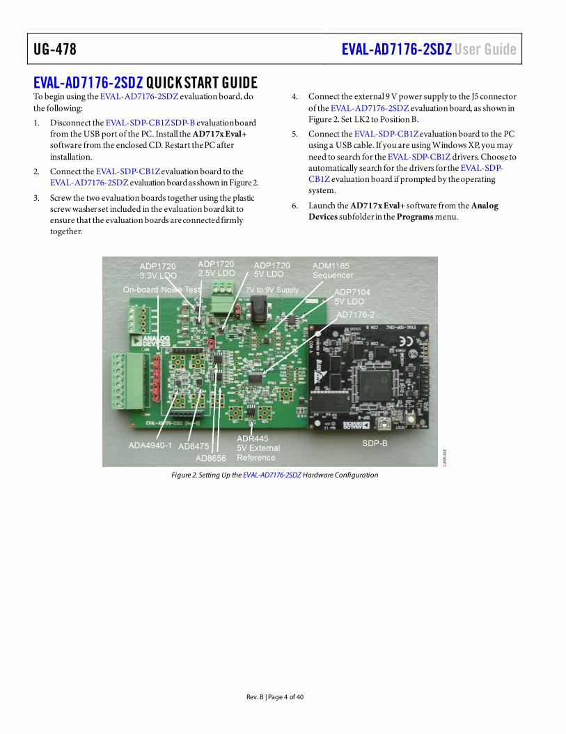
EVAL-AD7176-2SDZ QUICK START GUIDE To begin using the EVAL-AD7176-2SDZ evaluation board, do the following:
1. Disconnect the EVAL-SDP-CB1Z SDP-B evaluation board from the USB port of the PC. Install the AD717x Eval+ software from the enclosed CD. Restart the PC after installation.
2. Connect the EVAL-SDP-CB1Z evaluation board to the EVAL-AD7176-2SDZ evaluation board as shown in Figure 2.
3. Screw the two evaluation boards together using the plastic screw washer set included in the evaluation board kit to ensure that the evaluation boards are connected firmly together.
4. Connect the external 9 V power supply to the J5 connector of the EVAL-AD7176-2SDZ evaluation board, as shown in Figure 2. Set LK2 to Position B.
5. Connect the EVAL-SDP-CB1Z evaluation board to the PC using a USB cable. If you are using Windows XP, you may need to search for the EVAL-SDP-CB1Z drivers. Choose to automatically search for the drivers for the EVAL-SDP-CB1Z evaluation board if prompted by the operating system.
6. Launch the AD717x Eval+ software from the Analog Devices subfolder in the Programs menu.
1103
5-00
2
Figure 2. Setting Up the EVAL-AD7176-2SDZ Hardware Configuration
EVAL-AD7176-2SDZ User Guide UG-478
Rev. B | Page 5 of 40
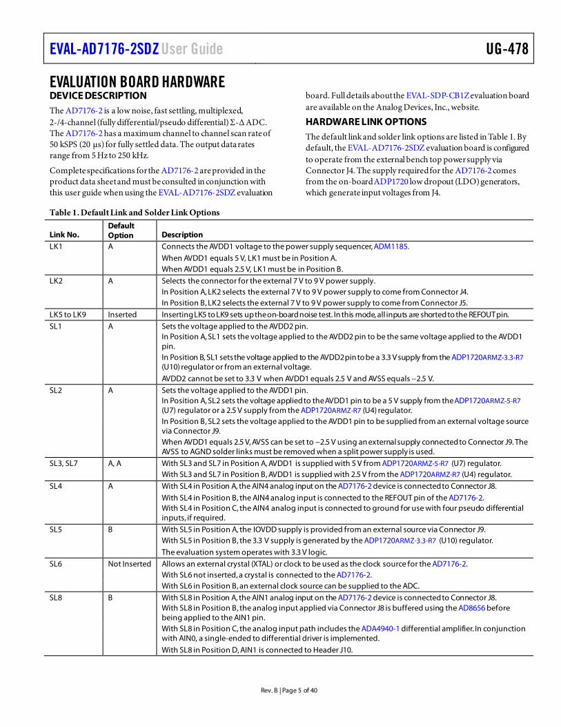
EVALUATION BOARD HARDWARE DEVICE DESCRIPTION The AD7176-2 is a low noise, fast settling, multiplexed, 2-/4-channel (fully differential/pseudo differential) Σ-Δ ADC. The AD7176-2 has a maximum channel to channel scan rate of 50 kSPS (20 µs) for fully settled data. The output data rates range from 5 Hz to 250 kHz.
Complete specifications for the AD7176-2 are provided in the product data sheet and must be consulted in conjunction with this user guide when using the EVAL-AD7176-2SDZ evaluation
board. Full details about the EVAL-SDP-CB1Z evaluation board are available on the Analog Devices, Inc., website.
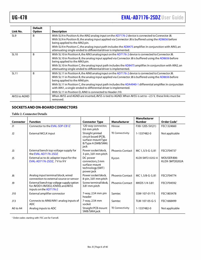
HARDWARE LINK OPTIONS The default link and solder link options are listed in Table 1. By default, the EVAL-AD7176-2SDZ evaluation board is configured to operate from the external bench top power supply via Connector J4. The supply required for the AD7176-2 comes from the on-board ADP1720 low dropout (LDO) generators, which generate input voltages from J4.
Table 1. Default Link and Solder Link Options
Link No. Default Option Description
LK1 A Connects the AVDD1 voltage to the power supply sequencer, ADM1185.
When AVDD1 equals 5 V, LK1 must be in Position A. When AVDD1 equals 2.5 V, LK1 must be in Position B.
LK2 A Selects the connector for the external 7 V to 9 V power supply. In Position A, LK2 selects the external 7 V to 9 V power supply to come from Connector J4. In Position B, LK2 selects the external 7 V to 9 V power supply to come from Connector J5.
LK5 to LK9 Inserted Inserting LK5 to LK9 sets up the on-board noise test. In this mode, all inputs are shorted to the REFOUT pin.
SL1 A Sets the voltage applied to the AVDD2 pin. In Position A, SL1 sets the voltage applied to the AVDD2 pin to be the same voltage applied to the AVDD1
pin.
In Position B, SL1 sets the voltage applied to the AVDD2 pin to be a 3.3 V supply from the ADP1720ARMZ-3.3-R7 (U10) regulator or from an external voltage.
AVDD2 cannot be set to 3.3 V when AVDD1 equals 2.5 V and AVSS equals −2.5 V.
SL2 A Sets the voltage applied to the AVDD1 pin. In Position A, SL2 sets the voltage applied to the AVDD1 pin to be a 5 V supply from the ADP1720ARMZ-5-R7
(U7) regulator or a 2.5 V supply from the ADP1720ARMZ-R7 (U4) regulator.
In Position B, SL2 sets the voltage applied to the AVDD1 pin to be supplied from an external voltage source via Connector J9.
When AVDD1 equals 2.5 V, AVSS can be set to −2.5 V using an external supply connected to Connector J9. The AVSS to AGND solder links must be removed when a split power supply is used.
SL3, SL7 A, A With SL3 and SL7 in Position A, AVDD1 is supplied with 5 V from ADP1720ARMZ-5-R7 (U7) regulator. With SL3 and SL7 in Position B, AVDD1 is supplied with 2.5 V from the ADP1720ARMZ-R7 (U4) regulator.
SL4 A With SL4 in Position A, the AIN4 analog input on the AD7176-2 device is connected to Connector J8.
With SL4 in Position B, the AIN4 analog input is connected to the REFOUT pin of the AD7176-2. With SL4 in Position C, the AIN4 analog input is connected to ground for use with four pseudo differential
inputs, if required.
SL5 B With SL5 in Position A, the IOVDD supply is provided from an external source via Connector J9. With SL5 in Position B, the 3.3 V supply is generated by the ADP1720ARMZ-3.3-R7 (U10) regulator.
The evaluation system operates with 3.3 V logic.
SL6 Not Inserted Allows an external crystal (XTAL) or clock to be used as the clock source for the AD7176-2. With SL6 not inserted, a crystal is connected to the AD7176-2. With SL6 in Position B, an external clock source can be supplied to the ADC.
SL8 B With SL8 in Position A, the AIN1 analog input on the AD7176-2 device is connected to Connector J8. With SL8 in Position B, the analog input applied via Connector J8 is buffered using the AD8656 before
being applied to the AIN1 pin.
With SL8 in Position C, the analog input path includes the ADA4940-1 differential amplifier. In conjunction with AIN0, a single-ended to differential driver is implemented.
With SL8 in Position D, AIN1 is connected to Header J10.
UG-478 EVAL-AD7176-2SDZ User Guide
Rev. B | Page 6 of 40
Link No. Default Option Description
SL9 B With SL9 in Position A, the AIN2 analog input on the AD7176-2 device is connected to Connector J8. With SL9 in Position B, the analog input applied via Connector J8 is buffered using the AD8656 before
being applied to the AIN2 pin.
With SL9 in Position C, the analog input path includes the AD8475 amplifier. In conjunction with AIN3, an attenuating single-ended to differential driver is implemented.
SL10 B With SL10 in Position A, the AIN3 analog input on the AD7176-2 device is connected to Connector J8.
With SL10 in Position B, the analog input applied via Connector J8 is buffered using the AD8656 before being applied to the AIN3 pin.
With SL10 in Position C, the analog input path includes the AD8475 amplifier. In conjunction with AIN2, an attenuating single-ended to differential driver is implemented.
SL11 B With SL11 in Position A, the AIN0 analog input on the AD7176-2 device is connected to Connector J8. With SL11 in Position B, the analog input applied via Connector J8 is buffered using the AD8656 before
being applied to the AIN0 pin.
With SL11 in Position C, the analog input path includes the ADA4940-1 differential amplifier. In conjunction with AIN1, a single-ended to differential driver is implemented.
With SL11 in Position D, AIN0 is connected to Header J10.
AVSS to AGND When AVSS and AGND are inserted, AVSS is tied to AGND. When AVSS is set to −2.5 V, these links must be removed.
SOCKETS AND ON-BOARD CONNECTORS
Table 2. Connector Details
Connector Function Connector Type Manufacturer Manufacturer Number Order Code1
J1 Connector to the EVAL-SDP-CB1Z 120-way connector, 0.6 mm pitch
Hirose FX8-120S-SV(21) FEC1324660
J2 External MCLK input Straight printed circuit board (PCB), surface-mount Type B/Type A (SMB/SMA) jack
TE Connectivity 1-1337482-0 Not applicable
J3 External bench top voltage supply for the EVAL-AD7176-2SDZ
Power socket block, 3-pin, 3.81 mm pitch
Phoenix Contact MC 1, 5/3-G-3, 81 FEC3704737
J5 External ac to dc adapter input for the EVAL-AD7176-2SDZ, 7 V to 9 V
DC power connectors, 2 mm surface-mount technology (SMT) power jack
Kycon KLDX-SMT2-0202-A MOUSER 806-KLDX-SMT20202A
J6 Analog input terminal block, wired connection to external source or sensor
Power socket block, 8-pin, 3.81 mm pitch
Phoenix Contact MC 1, 5/8-G-3, 81 FEC3704774
J9 External bench top voltage supply option for AVDD1/AVDD2, IOVDD, and AVSS inputs on the AD7176-2
Screw terminal block, 3.81 mm pitch
Phoenix Contact MKDS 1/4-3.81 FEC3704592
J10 External amplifier connector 7-way, 2.54 mm pin header
Samtec SSW-107-01-T-S FEC1803478
J13 Connects to AIN0/AIN1 analog inputs of ADC
7-way, 2.54 mm socket
Samtec TLW-107-05-G-S FEC1668499
A0 to A4 Analog inputs to ADC Straight PCB mount SMB/SMA jack
TE Connectivity 1-1337482-0 Not applicable
1 Order codes starting with FEC are for Farnell.
EVAL-AD7176-2SDZ User Guide UG-478
Rev. B | Page 7 of 40
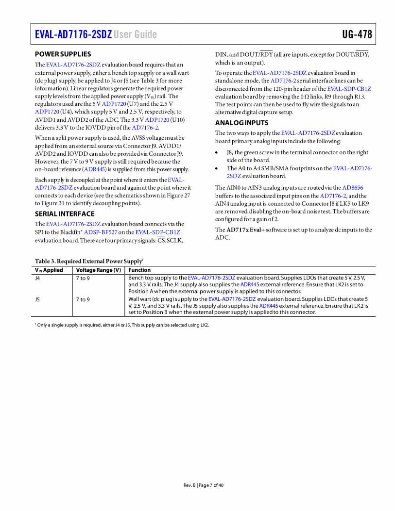
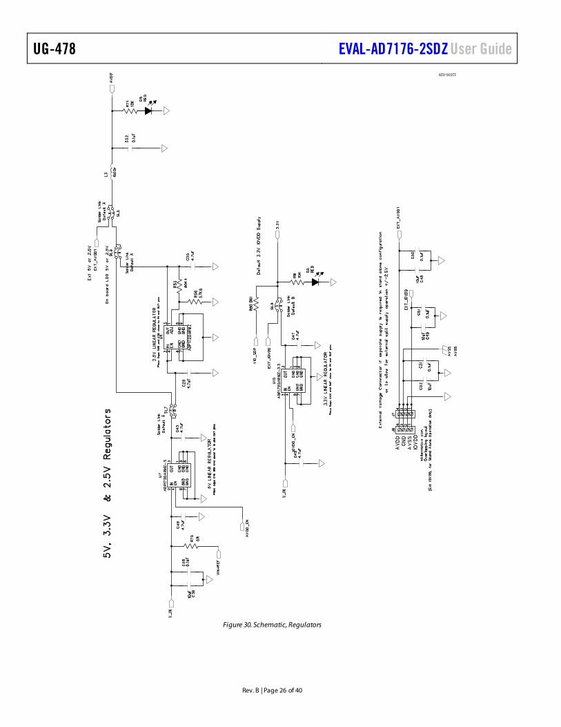
POWER SUPPLIES The EVAL-AD7176-2SDZ evaluation board requires that an external power supply, either a bench top supply or a wall wart (dc plug) supply, be applied to J4 or J5 (see Table 3 for more information). Linear regulators generate the required power supply levels from the applied power supply (VIN) rail. The regulators used are the 5 V ADP1720 (U7) and the 2.5 V ADP1720 (U4), which supply 5 V and 2.5 V, respectively, to AVDD1 and AVDD2 of the ADC. The 3.3 V ADP1720 (U10) delivers 3.3 V to the IOVDD pin of the AD7176-2.
When a split power supply is used, the AVSS voltage must be applied from an external source via Connector J9. AVDD1/ AVDD2 and IOVDD can also be provided via Connector J9. However, the 7 V to 9 V supply is still required because the on-board reference (ADR445) is supplied from this power supply.
Each supply is decoupled at the point where it enters the EVAL-AD7176-2SDZ evaluation board and again at the point where it connects to each device (see the schematics shown in Figure 27 to Figure 31 to identify decoupling points).
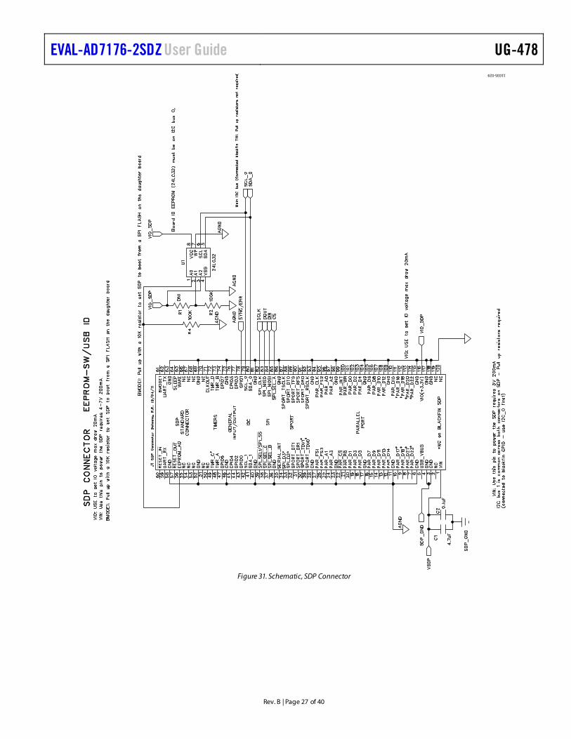
SERIAL INTERFACE The EVAL-AD7176-2SDZ evaluation board connects via the SPI to the Blackfin® ADSP-BF527 on the EVAL-SDP-CB1Z evaluation board. There are four primary signals: CS, SCLK,
DIN, and DOUT/RDY (all are inputs, except for DOUT/RDY, which is an output).
To operate the EVAL-AD7176-2SDZ evaluation board in standalone mode, the AD7176-2 serial interface lines can be disconnected from the 120-pin header of the EVAL-SDP-CB1Z evaluation board by removing the 0 Ω links, R9 through R13. The test points can then be used to fly wire the signals to an alternative digital capture setup.
ANALOG INPUTS The two ways to apply the EVAL-AD7176-2SDZ evaluation board primary analog inputs include the following:
• J8, the green screw in the terminal connector on the right side of the board.
• The A0 to A4 SMB/SMA footprints on the EVAL-AD7176-2SDZ evaluation board.
The AIN0 to AIN3 analog inputs are routed via the AD8656 buffers to the associated input pins on the AD7176-2, and the AIN4 analog input is connected to Connector J8 if LK5 to LK9 are removed, disabling the on-board noise test. The buffers are configured for a gain of 2.
The AD717x Eval+ software is set up to analyze dc inputs to the ADC.
Table 3. Required External Power Supply1 VIN Applied Voltage Range (V) Function J4 7 to 9 Bench top supply to the EVAL-AD7176-2SDZ evaluation board. Supplies LDOs that create 5 V, 2.5 V,
and 3.3 V rails. The J4 supply also supplies the ADR445 external reference. Ensure that LK2 is set to Position A when the external power supply is applied to this connector.
J5 7 to 9 Wall wart (dc plug) supply to the EVAL-AD7176-2SDZ evaluation board. Supplies LDOs that create 5 V, 2.5 V, and 3.3 V rails. The J5 supply also supplies the ADR445 external reference. Ensure that LK2 is set to Position B when the external power supply is applied to this connector.
1 Only a single supply is required, either J4 or J5. This supply can be selected using LK2.
UG-478 EVAL-AD7176-2SDZ User Guide
Rev. B | Page 8 of 40
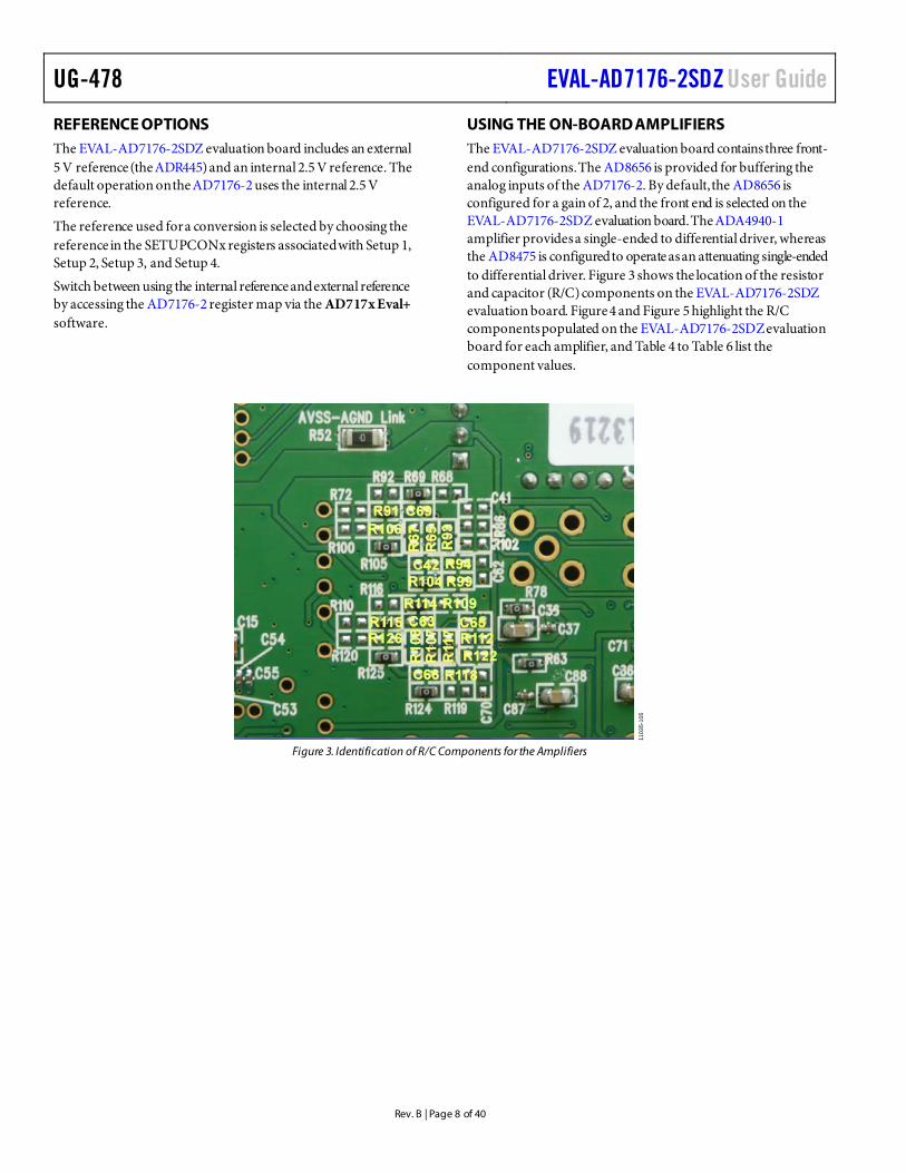
REFERENCE OPTIONS The EVAL-AD7176-2SDZ evaluation board includes an external 5 V reference (the ADR445) and an internal 2.5 V reference. The default operation on the AD7176-2 uses the internal 2.5 V reference.
The reference used for a conversion is selected by choosing the reference in the SETUPCONx registers associated with Setup 1, Setup 2, Setup 3, and Setup 4.
Switch between using the internal reference and external reference by accessing the AD7176-2 register map via the AD717x Eval+ software.
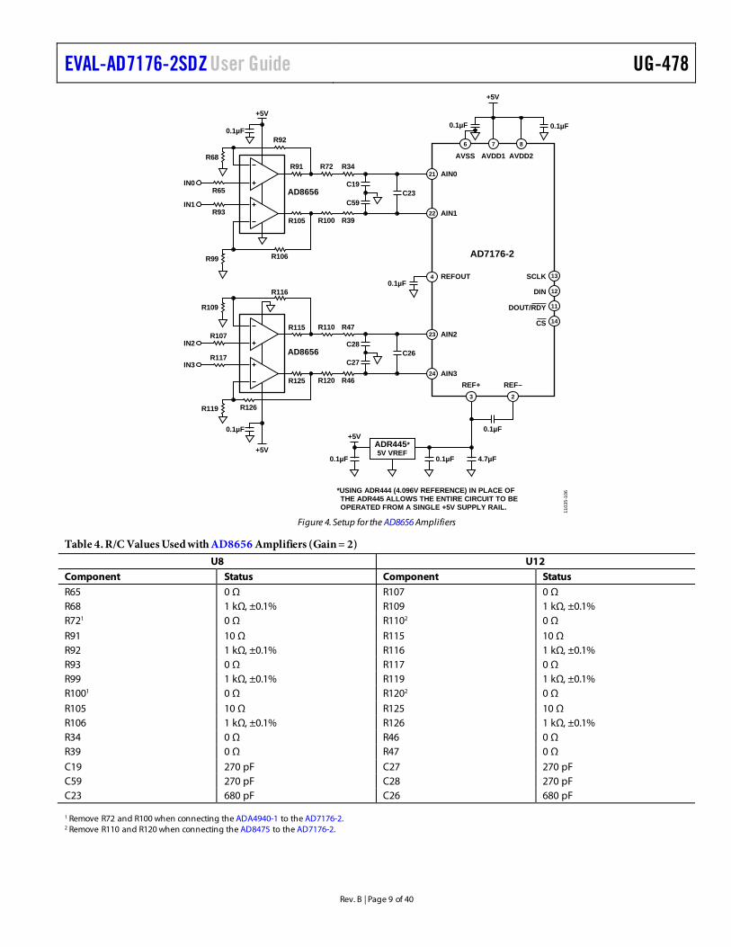
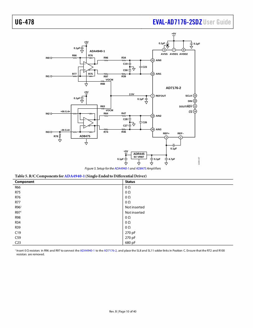
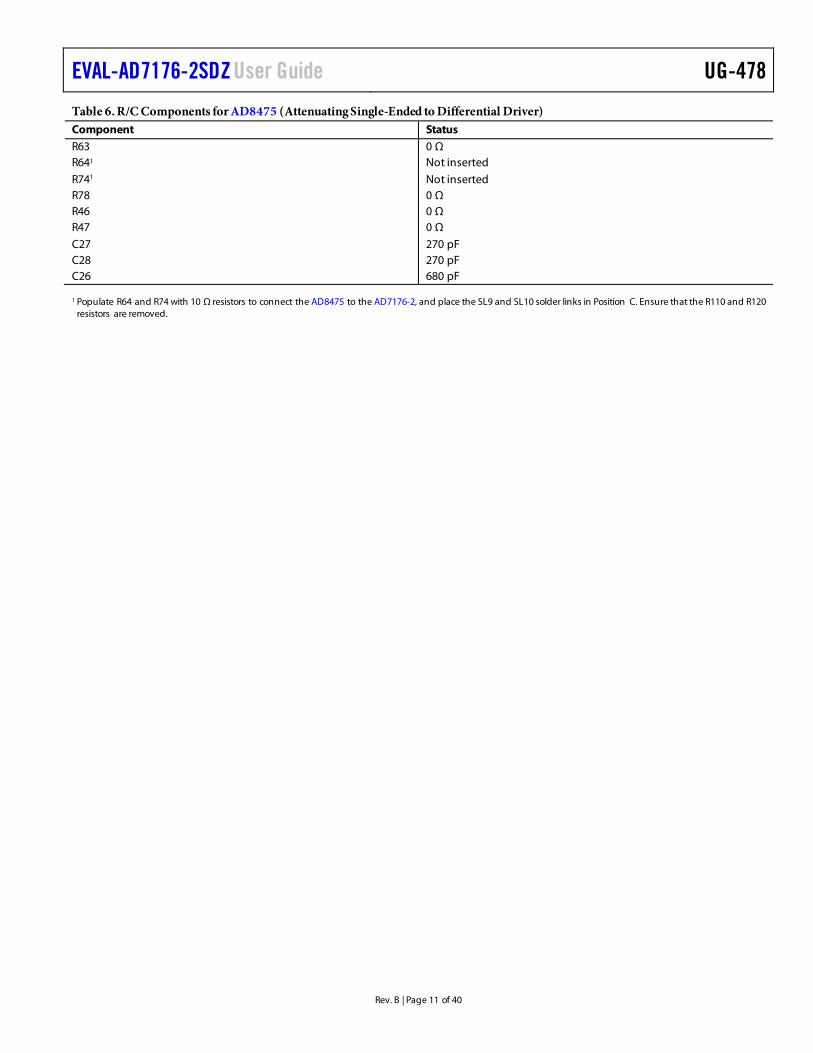
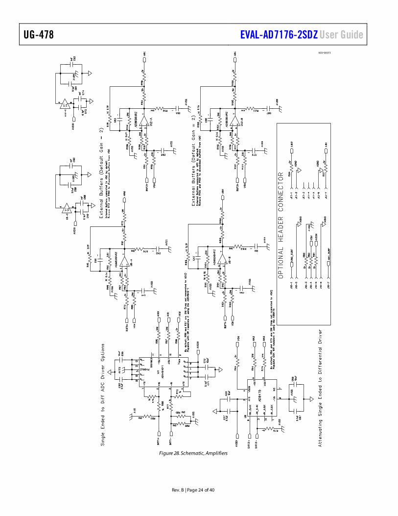
USING THE ON-BOARD AMPLIFIERS The EVAL-AD7176-2SDZ evaluation board contains three front-end configurations. The AD8656 is provided for buffering the analog inputs of the AD7176-2. By default, the AD8656 is configured for a gain of 2, and the front end is selected on the EVAL-AD7176-2SDZ evaluation board. The ADA4940-1 amplifier provides a single-ended to differential driver, whereas the AD8475 is configured to operate as an attenuating single-ended to differential driver. Figure 3 shows the location of the resistor and capacitor (R/C) components on the EVAL-AD7176-2SDZ evaluation board. Figure 4 and Figure 5 highlight the R/C components populated on the EVAL-AD7176-2SDZ evaluation board for each amplifier, and Table 4 to Table 6 list the component values.
1 103
5-10
5
Figure 3. Identification of R/C Components for the Amplifiers
EVAL-AD7176-2SDZ User Guide UG-478
Rev. B | Page 9 of 40
0.1µF
+5V
R91
R92
R105
R72
R100
R34
R39
R65
R93
AD8656
R68
R106R99
IN0
IN1
C19
C59C23
0.1µF
R119
+5V
R126
R115 R110 R47
R125 R120 R46
R107
R117AD8656
R116
R109
IN2
IN3
C28
C27C26
3
REF+2
REF–
21 AIN0
22 AIN1
23 AIN2
4 REFOUT
24 AIN3
6
AVSS7
AVDD18
AVDD2
0.1µF
AD7176-2
+5V
0.1µF 4.7µF0.1µF
ADR445*5V VREF
0.1µF
*USING ADR444 (4.096V REFERENCE) IN PLACE OFTHE ADR445 ALLOWS THE ENTIRE CIRCUIT TO BEOPERATED FROM A SINGLE +5V SUPPLY RAIL.
13
12
11
14
SCLK
DIN
CS
DOUT/RDY
1103
5-10
6
+5V
0.1µF 0.1µF
Figure 4. Setup for the AD8656 Amplifiers
Table 4. R/C Values Used with AD8656 Amplifiers (Gain = 2) U8 U12
Component Status Component Status R65 0 Ω R107 0 Ω R68 1 kΩ, ±0.1% R109 1 kΩ, ±0.1% R721 0 Ω R1102 0 Ω
R91 10 Ω R115 10 Ω R92 1 kΩ, ±0.1% R116 1 kΩ, ±0.1% R93 0 Ω R117 0 Ω R99 1 kΩ, ±0.1% R119 1 kΩ, ±0.1% R1001 0 Ω R1202 0 Ω
R105 10 Ω R125 10 Ω R106 1 kΩ, ±0.1% R126 1 kΩ, ±0.1% R34 0 Ω R46 0 Ω R39 0 Ω R47 0 Ω
C19 270 pF C27 270 pF C59 270 pF C28 270 pF C23 680 pF C26 680 pF 1 Remove R72 and R100 when connecting the ADA4940-1 to the AD7176-2. 2 Remove R110 and R120 when connecting the AD8475 to the AD7176-2.
UG-478 EVAL-AD7176-2SDZ User Guide
Rev. B | Page 10 of 40
1103
5-10
7
R96
R97
R34
R39
C19
C59C23
R64 R47
R74 R46
C28
C27C26
3
REF+2
REF–
21 AIN0
22 AIN1
23 AIN2
4 REFOUT
24 AIN3
6
AVSS7
AVDD18
AVDD2
0.1µF
+5V
0.1µF 0.1µF
AD7176-2
+5V
0.1µF 4.7µF0.1µF
ADR4455V VREF
0.1µF
13
12
11
14
SCLK
DIN
CS
DOUT/RDY
0.1µF
+5V
IN0
IN1
R76R66
R75R77
0.1µF
+5V
IN2
IN3AD8475
ADA4940-1
R98
R63
VOCM
VOCM
2.5V
R78
+IN 0.4×
–IN 0.4×
Figure 5. Setup for the ADA4940-1 and AD8475 Amplifiers
Table 5. R/C Components for ADA4940-1 (Single-Ended to Differential Driver) Component Status
R66 0 Ω R75 0 Ω R76 0 Ω R77 0 Ω R961 Not inserted
R971 Not inserted R98 0 Ω R34 0 Ω R39 0 Ω
C19 270 pF C59 270 pF C23 680 pF 1 Insert 0 Ω resistors in R96 and R97 to connect the ADA4940-1 to the AD7176-2, and place the SL8 and SL11 solder links in Position C. Ensure that the R72 and R100
resistors are removed.
EVAL-AD7176-2SDZ User Guide UG-478
Rev. B | Page 11 of 40
Table 6. R/C Components for AD8475 (Attenuating Single-Ended to Differential Driver) Component Status R63 0 Ω R641 Not inserted
R741 Not inserted R78 0 Ω R46 0 Ω R47 0 Ω
C27 270 pF C28 270 pF C26 680 pF 1 Populate R64 and R74 with 10 Ω resistors to connect the AD8475 to the AD7176-2, and place the SL9 and SL10 solder links in Position C. Ensure that the R110 and R120
resistors are removed.
UG-478 EVAL-AD7176-2SDZ User Guide
Rev. B | Page 12 of 40
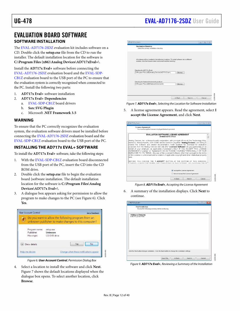
EVALUATION BOARD SOFTWARE SOFTWARE INSTALLATION The EVAL-AD7176-2SDZ evaluation kit includes software on a CD. Double click the setup.exe file from the CD to run the installer. The default installation location for the software is C:\Program Files (x86)\Analog Devices\AD717xEval+\.
Install the AD717x Eval+ software before connecting the EVAL-AD7176-2SDZ evaluation board and the EVAL-SDP-CB1Z evaluation board to the USB port of the PC to ensure that the evaluation system is correctly recognized when connected to the PC. Install the following two parts:
1. AD717x Eval+ software installation 2. AD717x Eval+ Dependencies
a. EVAL-SDP-CB1Z board drivers b. Ssrc SVG Plugin c. Microsoft .NET Framework 3.5
WARNING To ensure that the PC correctly recognizes the evaluation system, the evaluation software drivers must be installed before connecting the EVAL-AD7176-2SDZ evaluation board and the EVAL-SDP-CB1Z evaluation board to the USB port of the PC.
INSTALLING THE AD717X EVAL+ SOFTWARE To install the AD717x Eval+ software, take the following steps:
1. With the EVAL-SDP-CB1Z evaluation board disconnected from the USB port of the PC, insert the CD into the CD ROM drive.
2. Double click the setup.exe file to begin the evaluation board software installation. The default installation location for the software is C:\Program Files\Analog Devices\AD717x Eval+\.
3. A dialogue box appears asking for permission to allow the program to make changes to the PC (see Figure 6). Click Yes.
1103
5-00
3
Figure 6. User Account Control, Permission Dialog Box
4. Select a location to install the software and click Next. Figure 7 shows the default locations displayed when the dialogue box opens. To select another location, click Browse.
1103
5-00
4
Figure 7. AD717x Eval+, Selecting the Location for Software Installation
5. A license agreement appears. Read the agreement, select I accept the License Agreement, and click Next.
1103
5-00
5
Figure 8. AD717x Eval+, Accepting the License Agreement
6. A summary of the installation displays. Click Next to continue.
1103
5-00
6
Figure 9. AD717x Eval+, Reviewing a Summary of the Installation
EVAL-AD7176-2SDZ User Guide UG-478
Rev. B | Page 13 of 40
7. The message in Figure 10 appears when the installation is complete. Click Next to continue.
1103
5-00
7
Figure 10. AD717x Eval+ Installation Complete
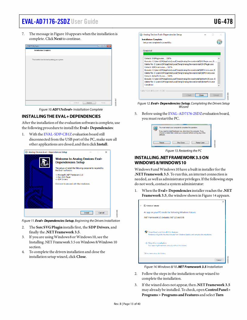
INSTALLING THE EVAL+ DEPENDENCIES After the installation of the evaluation software is complete, use the following procedure to install the Eval+ Dependencies:
1. With the EVAL-SDP-CB1Z evaluation board still disconnected from the USB port of the PC, make sure all other applications are closed, and then click Install.
1103
5-00
8
Figure 11. Eval+ Dependencies Setup, Beginning the Drivers Installation
2. The Ssrc SVG Plugin installs first, the SDP Drivers, and finally the .NET Framework 3.5.
3. If you are using Windows 8 or Windows 10, see the Installing .NET Framework 3.5 on Windows 8/Windows 10 section.
4. To complete the drivers installation and close the installation setup wizard, click Close.
1 103
5-00
9
Figure 12. Eval+ Dependencies Setup, Completing the Drivers Setup
Wizard
5. Before using the EVAL-AD7176-2SDZ evaluation board, you must restart the PC.
1103
5-01
0
Figure 13. Restarting the PC
INSTALLING .NET FRAMEWORK 3.5 ON WINDOWS 8/WINDOWS 10 Windows 8 and Windows 10 have a built in installer for the .NET Framework 3.5. To run this, an internet connection is needed, as well as administrator privileges. If the following steps do not work, contact a system administrator:
1. When the Eval+ Dependencies installer reaches the .NET Framework 3.5, the window shown in Figure 14 appears.
1103
5-01
1
Figure 14. Windows 8/10 .NET Framework 3.5 Installation
2. Follow the steps in the installation setup wizard to complete the installation.
3. If the wizard does not appear, then .NET Framework 3.5 may already be installed. To check, open Control Panel > Programs > Programs and Features and select Turn
UG-478 EVAL-AD7176-2SDZ User Guide
Rev. B | Page 14 of 40
Windows features on or off. In the window that appears, look for .NET Framework 3.5 and check that it is enabled.
SETTING UP THE SYSTEM FOR DATA CAPTURE After completing the steps in the Evaluation Board Hardware and the Software Installation sections, set up the system for data capture using the following:
1. Allow the Found New Hardware Wizard to run after the EVAL-SDP-CB1Z evaluation board is connected to the PC. If using Windows XP, search for the EVAL-SDP-CB1Z drivers. Choose to automatically search for the drivers if prompted by the operating system.
2. Check that the EVAL-AD7176-2SDZ evaluation board is connecting to the PC correctly using the Device Manager. Access the Device Manager by completing the following steps: a. Right click My Computer and then click Manage. b. A dialog box appears asking for permission to allow
the program to make changes to the PC. Click Yes. c. The Computer Management window appears. Click
Device Manager from the list of System Tools (see Figure 15).
d. The EVAL-SDP-CB1Z evaluation board appears under ADI Development Tools, which indicates that the driver software has installed and that the EVAL-SDP-CB1Z evaluation board is connecting to the PC correctly.
1103
5-01
2
Figure 15. Device Manager, Checking the Board Connects to the PC
Correctly
LAUNCHING THE SOFTWARE After completing the steps in the Setting Up the System for Data Capture section, launch the AD717x Eval+ software using the following steps:
1. From the Start menu, click Programs > Analog Devices > AD717x_Eval+ > AD717x Eval+.
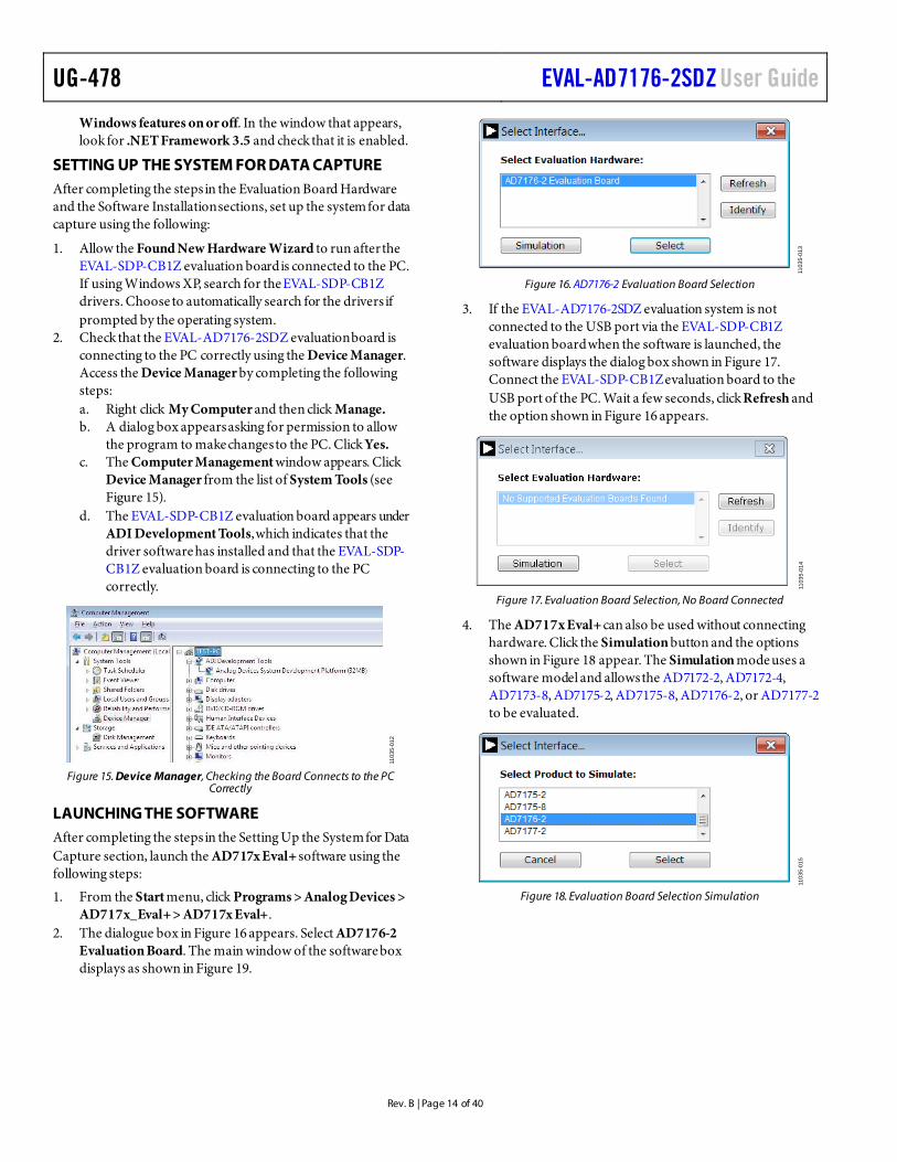
2. The dialogue box in Figure 16 appears. Select AD7176-2 Evaluation Board. The main window of the software box displays as shown in Figure 19.
1103
5-01
3
Figure 16. AD7176-2 Evaluation Board Selection
3. If the EVAL-AD7176-2SDZ evaluation system is not connected to the USB port via the EVAL-SDP-CB1Z evaluation board when the software is launched, the software displays the dialog box shown in Figure 17. Connect the EVAL-SDP-CB1Z evaluation board to the USB port of the PC. Wait a few seconds, click Refresh and the option shown in Figure 16 appears.
1103
5-01
4
Figure 17. Evaluation Board Selection, No Board Connected
4. The AD717x Eval+ can also be used without connecting hardware. Click the Simulation button and the options shown in Figure 18 appear. The Simulation mode uses a software model and allows the AD7172-2, AD7172-4, AD7173-8, AD7175-2, AD7175-8, AD7176-2, or AD7177-2 to be evaluated.
1103
5-01
5
Figure 18. Evaluation Board Selection Simulation
EVAL-AD7176-2SDZ User Guide UG-478
Rev. B | Page 15 of 40
EVALUATION BOARD SOFTWARE OPERATION
1103
5-01
6
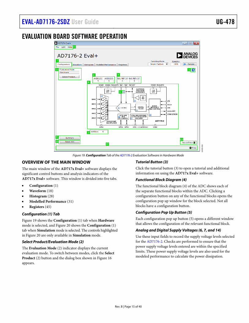
Figure 19. Configuration Tab of the AD7176-2 Evaluation Software in Hardware Mode
OVERVIEW OF THE MAIN WINDOW The main window of the AD717x Eval+ software displays the significant control buttons and analysis indicators of the AD717x Eval+ software. This window is divided into five tabs.
Configuration (1) Waveform (18) Histogram (28) Modelled Performance (31) Registers (45)
Configuration (1) Tab
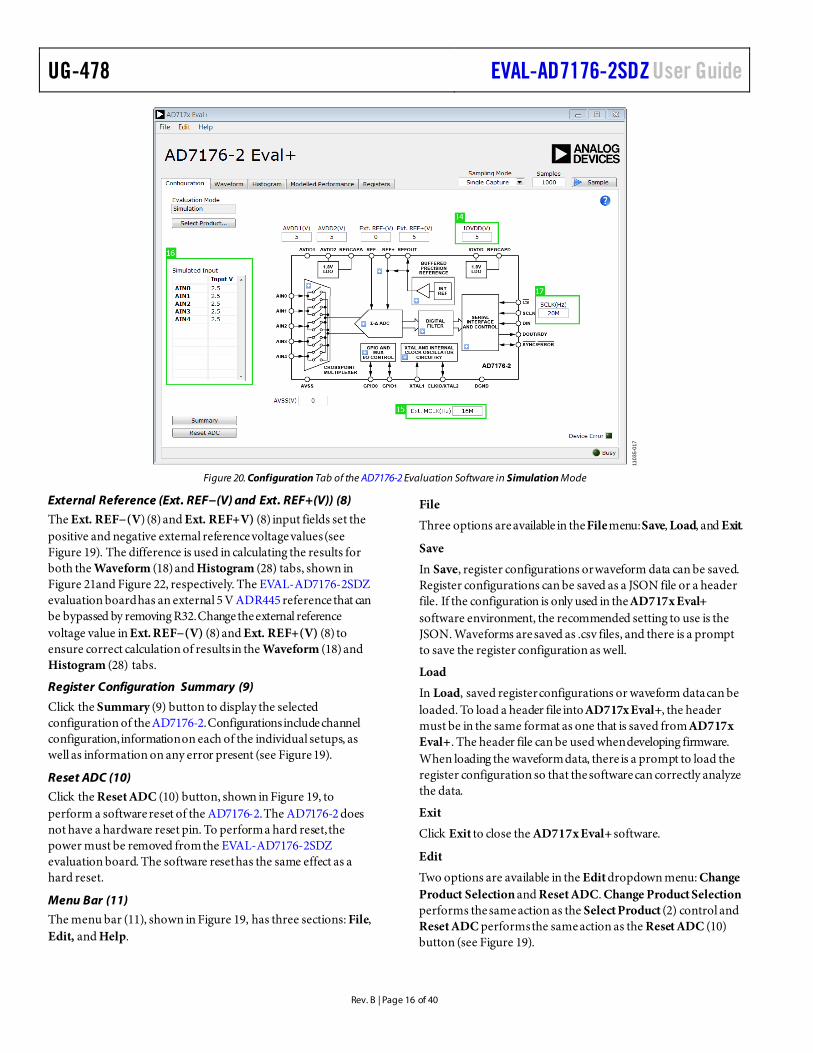
Figure 19 shows the Configuration (1) tab when Hardware mode is selected, and Figure 20 shows the Configuration (1) tab when Simulation mode is selected. The controls highlighted in Figure 20 are only available in Simulation mode.
Select Product/Evaluation Mode (2)
The Evaluation Mode (2) indicator displays the current evaluation mode. To switch between modes, click the Select Product (2) button and the dialog box shown in Figure 16 appears.
Tutorial Button (3)
Click the tutorial button (3) to open a tutorial and additional information on using the AD717x Eval+ software.
Functional Block Diagram (4)
The functional block diagram (4) of the ADC shows each of the separate functional blocks within the ADC. Clicking a configuration button on any of the functional blocks opens the configuration pop up window for the block selected. Not all blocks have a configuration button.
Configuration Pop Up Button (5)
Each configuration pop up button (5) opens a different window that allows the configuration of the relevant functional block.
Analog and Digital Supply Voltages (6, 7, and 14)
Use these input fields to record the supply voltage levels selected for the AD7176-2. Checks are performed to ensure that the power supply voltage levels entered are within the specified limits. These power supply voltage levels are also used for the modeled performance to calculate the power dissipation.
UG-478 EVAL-AD7176-2SDZ User Guide
Rev. B | Page 16 of 40
1103
5-01
7
Figure 20. Configuration Tab of the AD7176-2 Evaluation Software in Simulation Mode
External Reference (Ext. REF−(V) and Ext. REF+(V)) (8)
The Ext. REF−(V) (8) and Ext. REF+V) (8) input fields set the positive and negative external reference voltage values (see Figure 19). The difference is used in calculating the results for both the Waveform (18) and Histogram (28) tabs, shown in Figure 21and Figure 22, respectively. The EVAL-AD7176-2SDZ evaluation board has an external 5 V ADR445 reference that can be bypassed by removing R32. Change the external reference voltage value in Ext. REF−(V) (8) and Ext. REF+(V) (8) to ensure correct calculation of results in the Waveform (18) and Histogram (28) tabs.
Register Configuration Summary (9)
Click the Summary (9) button to display the selected configuration of the AD7176-2. Configurations include channel configuration, information on each of the individual setups, as well as information on any error present (see Figure 19).
Reset ADC (10)
Click the Reset ADC (10) button, shown in Figure 19, to perform a software reset of the AD7176-2. The AD7176-2 does not have a hardware reset pin. To perform a hard reset, the power must be removed from the EVAL-AD7176-2SDZ evaluation board. The software reset has the same effect as a hard reset.
Menu Bar (11)
The menu bar (11), shown in Figure 19, has three sections: File, Edit, and Help.
File
Three options are available in the File menu: Save, Load, and Exit.
Save
In Save, register configurations or waveform data can be saved. Register configurations can be saved as a JSON file or a header file. If the configuration is only used in the AD717x Eval+ software environment, the recommended setting to use is the JSON. Waveforms are saved as .csv files, and there is a prompt to save the register configuration as well.
Load
In Load, saved register configurations or waveform data can be loaded. To load a header file into AD717x Eval+, the header must be in the same format as one that is saved from AD717x Eval+. The header file can be used when developing firmware. When loading the waveform data, there is a prompt to load the register configuration so that the software can correctly analyze the data.
Exit
Click Exit to close the AD717x Eval+ software.
Edit
Two options are available in the Edit dropdown menu: Change Product Selection and Reset ADC. Change Product Selection performs the same action as the Select Product (2) control and Reset ADC performs the same action as the Reset ADC (10) button (see Figure 19).
EVAL-AD7176-2SDZ User Guide UG-478
Rev. B | Page 17 of 40
Help
The Help dropdown menu provides links to extra information about the AD7176-2, which includes links to the product page, EVAL-AD7176-2SDZ evaluation board user guide, data sheet, and No OS drivers. Selecting the AD717x Eval+ tutorial opens the tutorial outlined in the Tutorial Button (3) section. For details on the version of the software, the About option opens a dialog box displaying the current version of the software and the relevant licenses.
Status Bar (12)
The status bar (12) displays the busy indicator and status updates, such as Analysis Completed and Reset Completed during software use (see Figure 19).
Device Error (13)
The Device Error (13) light emitting diode (LED) icon, shown in Figure 19, illuminates when a when an ADC error is detected or when a cyclic redundancy check (CRC) error occurs. The CRC functionality on the AD7176-2 is disabled by default and must be enabled for this indicator to work. More specific information on the error can be found in the Register Configuration Summary (9) section.
External MCLK Frequency (15)
This field sets the external MCLK frequency (15) (see Figure 20). The external MCLK frequency is only visible on the front panel when an external clock source is selected by the ADC. The external MCLK frequency is used by the functional model for the Modelled Performance (31) tab, shown in Figure 23.
Analog Input Voltage (16)
These input fields are only available when the AD717x Eval+ software is executed in Simulation mode. These inputs allow
the analog input voltages (16) to be set and can be changed at any time while in Simulation mode (see Figure 20).
External SCLK Frequency (17)
This input field sets the external SCLK frequency (17) for the SPI interface. This field is only available in Simulation mode to determine if the SCLK frequency (17) is within the permitted range (see Figure 20).
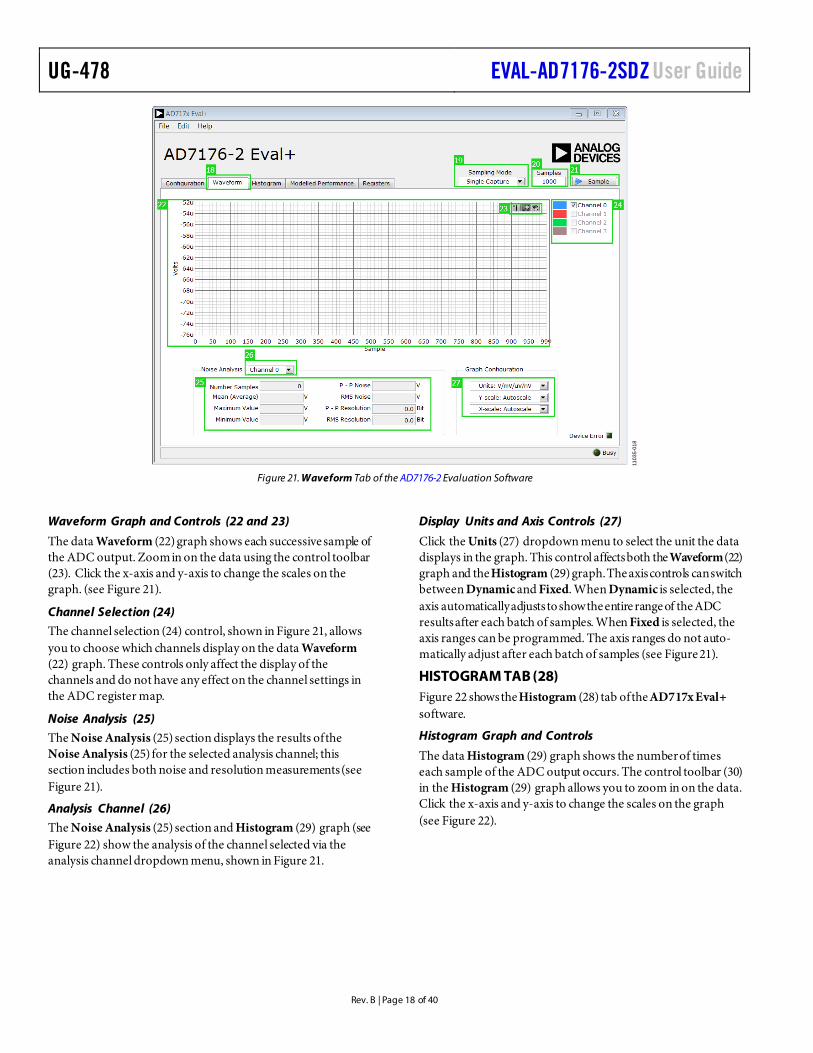
WAVEFORM TAB (18) Figure 21 shows the Waveform (18) tab of the AD717x Eval+ Software.
Sampling Mode (19)
This control, shown in Figure 21, is unrelated to the ADC mode. A defined sample set can be captured in a single capture, or batches of samples can be continuously gathered in a repeated capture. Data logging that runs like repeated capture but posts the results to a .csv file can also be selected. When saving, the .csv file prompts to save the register configuration, which is necessary for the analysis of the data to load back into the software.
Samples (20)
The Samples (20) numeric control sets the number of Samples (20) gathered per batch. Single capture returns the number entered in the Samples (20) control. A repeated capture keeps returning batches of the number in Samples (20) until stopped (see Figure 21).
Sample (21)
Click the Sample (21) button to start gathering ADC results. Results appear in the Waveform (22) graph. Both the Sample (21) button and the Waveform (22) graph are shown in Figure 21.
UG-478 EVAL-AD7176-2SDZ User Guide
Rev. B | Page 18 of 40
1103
5-01
8
Figure 21. Waveform Tab of the AD7176-2 Evaluation Software
Waveform Graph and Controls (22 and 23)
The data Waveform (22) graph shows each successive sample of the ADC output. Zoom in on the data using the control toolbar (23). Click the x-axis and y-axis to change the scales on the graph. (see Figure 21).
Channel Selection (24)
The channel selection (24) control, shown in Figure 21, allows you to choose which channels display on the data Waveform (22) graph. These controls only affect the display of the channels and do not have any effect on the channel settings in the ADC register map.
Noise Analysis (25)
The Noise Analysis (25) section displays the results of the Noise Analysis (25) for the selected analysis channel; this section includes both noise and resolution measurements (see Figure 21).
Analysis Channel (26)
The Noise Analysis (25) section and Histogram (29) graph (see Figure 22) show the analysis of the channel selected via the analysis channel dropdown menu, shown in Figure 21.
Display Units and Axis Controls (27)
Click the Units (27) dropdown menu to select the unit the data displays in the graph. This control affects both the Waveform (22) graph and the Histogram (29) graph. The axis controls can switch between Dynamic and Fixed. When Dynamic is selected, the axis automatically adjusts to show the entire range of the ADC results after each batch of samples. When Fixed is selected, the axis ranges can be programmed. The axis ranges do not auto-matically adjust after each batch of samples (see Figure 21).
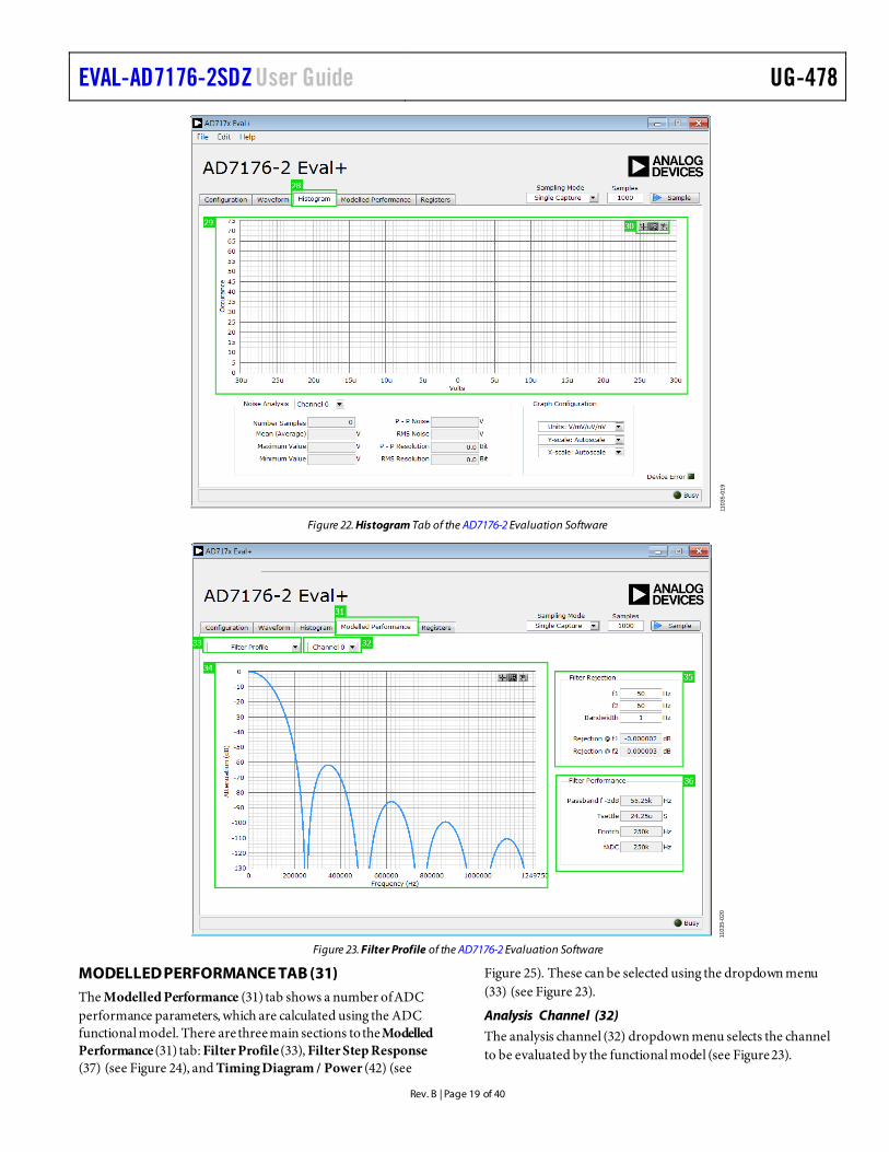
HISTOGRAM TAB (28) Figure 22 shows the Histogram (28) tab of the AD717x Eval+ software.
Histogram Graph and Controls
The data Histogram (29) graph shows the number of times each sample of the ADC output occurs. The control toolbar (30) in the Histogram (29) graph allows you to zoom in on the data. Click the x-axis and y-axis to change the scales on the graph (see Figure 22).
EVAL-AD7176-2SDZ User Guide UG-478
Rev. B | Page 19 of 40
1103
5-01
9
Figure 22. Histogram Tab of the AD7176-2 Evaluation Software
1103
5-02
0
Figure 23. Filter Profile of the AD7176-2 Evaluation Software
MODELLED PERFORMANCE TAB (31) The Modelled Performance (31) tab shows a number of ADC performance parameters, which are calculated using the ADC functional model. There are three main sections to the Modelled Performance (31) tab: Filter Profile (33), Filter Step Response (37) (see Figure 24), and Timing Diagram / Power (42) (see
Figure 25). These can be selected using the dropdown menu (33) (see Figure 23).
Analysis Channel (32)
The analysis channel (32) dropdown menu selects the channel to be evaluated by the functional model (see Figure 23).
UG-478 EVAL-AD7176-2SDZ User Guide
Rev. B | Page 20 of 40
Filter Profile (33)
This dropdown menu gives the ability to switch between the three sections of the Modelled Performance (31) tab. Figure 23 shows the tab when Filter Profile (33) is selected.
Filter Profile Graph (34)
This graph shows the frequency response for the selected digital filter. The graph controls give the ability to zoom in on the data. Click the x-axis and y-axis to change the scales on the graph (see Figure 23).
Filter Rejection (35)
This section shows the rejection/attenuation of the digital filter over the Rejection @ f1 bandwidth and the Rejection @ f2 bandwidth in decibels. The f1, f2, and Bandwidth values can be changed (see Figure 23).
Filter Performance (36)
This section shows timing information about the data rate of the selected output. The Filter Performance (36) shows the ADC initial settling time (Tsettle), the first frequency notch (Fnotch), and the actual sampling frequency (fADC) (see Figure 23).
Filter Step Response (37)
This dropdown menu gives the ability to switch between the three sections of the Modelled Performance (31) tab (see (see Figure 23). Figure 24 shows the tab when Filter Step Response (37) is selected.
Step Response Graph (38)
This graph shows how long the filter takes to settle when the voltage is stepped from one voltage to the next. For this analysis, it is assumed the ADC is continuously converting on only one channel (see Figure 24).
Step Configuration (39)
Step Configuration (39) gives the ability to set the Voltage before Step, the Voltage after Step, and the Step Position. Step Position is set as a percentage where 0% is 1/fADC and 100% is 2/fADC (see Figure 24).
Step Response (40)
This section shows timing information about the data rate of the output selected output. The Step Response (40) shows the actual sampling frequency, fADC, the ADC initial settling time (tSettle), and the settling time between conversions, 1/fADC (see Figure 24).
Graph Units (41)
Use this control to switch the step response between Percentages, Volts, and Codes (see Figure 24).
1103
5-02
1
Figure 24. Filter Step Response of the AD7176-2 Evaluation Software
EVAL-AD7176-2SDZ User Guide UG-478
Rev. B | Page 21 of 40
1103
5-02
2
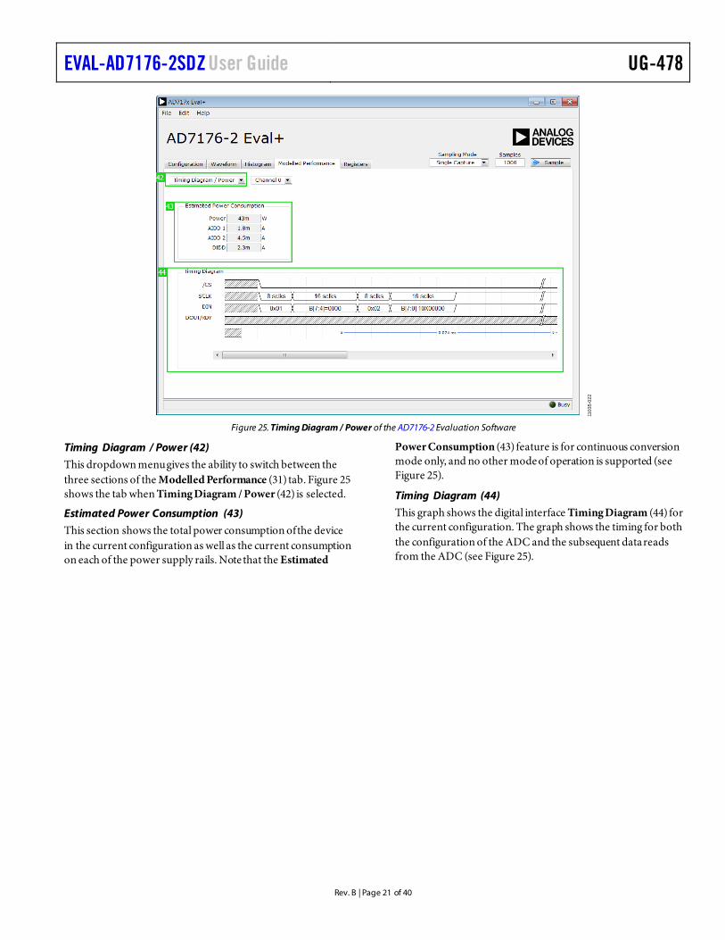
Figure 25. Timing Diagram / Power of the AD7176-2 Evaluation Software
Timing Diagram / Power (42)
This dropdown menu gives the ability to switch between the three sections of the Modelled Performance (31) tab. Figure 25 shows the tab when Timing Diagram / Power (42) is selected.
Estimated Power Consumption (43)
This section shows the total power consumption of the device in the current configuration as well as the current consumption on each of the power supply rails. Note that the Estimated
Power Consumption (43) feature is for continuous conversion mode only, and no other mode of operation is supported (see Figure 25).
Timing Diagram (44)
This graph shows the digital interface Timing Diagram (44) for the current configuration. The graph shows the timing for both the configuration of the ADC and the subsequent data reads from the ADC (see Figure 25).
UG-478 EVAL-AD7176-2SDZ User Guide
Rev. B | Page 22 of 40
1103
5-02
3
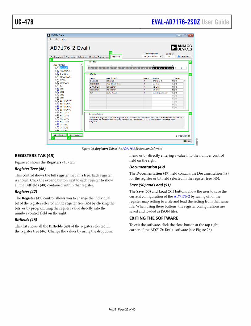
Figure 26. Registers Tab of the AD7176-2 Evaluation Software
REGISTERS TAB (45) Figure 26 shows the Registers (45) tab.
Register Tree (46)
This control shows the full register map in a tree. Each register is shown. Click the expand button next to each register to show all the Bitfields (48) contained within that register.
Register (47)
The Register (47) control allows you to change the individual bit of the register selected in the register tree (46) by clicking the bits, or by programming the register value directly into the number control field on the right.
Bitfields (48)
This list shows all the Bitfields (48) of the register selected in the register tree (46). Change the values by using the dropdown
menu or by directly entering a value into the number control field on the right.
Documentation (49)
The Documentation (49) field contains the Documentation (49) for the register or bit field selected in the register tree (46).
Save (50) and Load (51)
The Save (50) and Load (51) buttons allow the user to save the current configuration of the AD7176-2 by saving off of the register map setting to a file and load the setting from that same file. When using these buttons, the register configurations are saved and loaded as JSON files.
EXITING THE SOFTWARE To exit the software, click the close button at the top right corner of the AD717x Eval+ software (see Figure 26).
EVAL-AD7176-2SDZ User Guide UG-478
Rev. B | Page 23 of 40
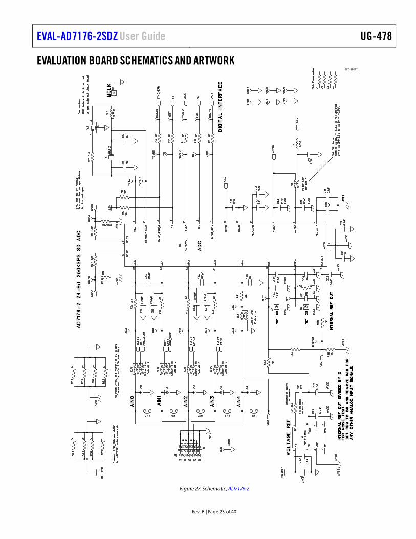
EVALUATION BOARD SCHEMATICS AND ARTWORK
11035-025
Figure 27. Schematic, AD7176-2
UG-478 EVAL-AD7176-2SDZ User Guide
Rev. B | Page 24 of 40
11035-026
Figure 28. Schematic, Amplifiers
EVAL-AD7176-2SDZ User Guide UG-478
Rev. B | Page 25 of 40
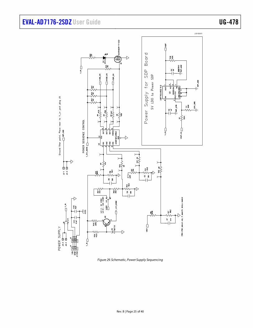
11035-027
Figure 29. Schematic, Power Supply Sequencing
UG-478 EVAL-AD7176-2SDZ User Guide
Rev. B | Page 26 of 40
11035-028
Figure 30. Schematic, Regulators
EVAL-AD7176-2SDZ User Guide UG-478
Rev. B | Page 27 of 40
11035-029
Figure 31. Schematic, SDP Connector
UG-478 EVAL-AD7176-2SDZ User Guide
Rev. B | Page 28 of 40
1103
5-03
0
1
1
121
122
1
2
3
4
12 3
45
1
2
5
6
1
2
3
12
1
2
12
34
5
12
34
5
12
34
5
12
34
5
123
4 5
123
4 51
23
4 5
1
2
3
4
1
1
1
1
1
1
1
1
11
11
11
1 1
1 1
1 1
1
1
1
1
1
1
1
1
1
1
1 1
1 1
1 1
1 1
1 1
1
2
3
4
5
6
7
8
1
2
3
4
5
6
7
8
1
2
1
2
1
2
1
2
1
2
1
2
12
12
12
12
1
1
1
1
1
2
1
2
1
2
1
2
1
2
123
123
1
2
3
1
2
1
2
1 212
1
2
1 2
12
3
1
1
1 2
12
1 2
1 2
1 2
1 2
1 2
12
1 212
1 2
1 2
12
1 21 2
1 2
1 2
12
12
12
1 2
12
1 2 3 4 5 6 7
1 2 3 4 5 6 7
1 2
1 2
1 2
1 2
1 2
12
12
1 2
1 2
1 2
1 2
1 2
1 2
12
1 2
1 2
1 2
1 2
1 2
1 2
1 2
1 2
12
12
1 2 1 2
1 2
12
12
12
12
1 2
1 2
1 2
12
1 2
1 2
1
1
1
1
1
1
2
1
2
K A
K
A
1
2
3
45
6
7
8
9
10
11
1213
14
15
16
17
18
1920
21
22
23
24
25
2627
28
29
30
31
32
33
3435
36
37
38
39
40
4142
43
44
45
46
47
48
4950
51
52
53
54
55
5657
58
59
6061
62
63
6465
66
67
68
69
70
7172
73
74
75
76
77
78
7980
81
82
83
84
85
8687
88
89
90
91
92
93
9495
96
97
98
99
100
101102
103
104
105
106
107
108109
110
111
112
113
114
115
116117
118
119
120
121
122
1
2
3
4
1 2 3 45678
1 2
1
2
12 3
45
123456
78910
1
2
1
2
1
2
1 2
1
2
1 2 3
1
2 3
4
5
6
1
2
3
1 2
1 2
B E
C
1 2
1
2
1 2
1 2
1 2
1 2
1 2
1
2
1 2
1
2
1
2
1
2
1 2
12
12
1 2
3
12
34
5
12
34
5
12
34
5
12
34
5
123
4 5
123
4 51
23
4 5
1
2
3
4
1
1
1
1
1
1
1
1
11
11
11
1 1
1 1
1 1
1
1
1
1
1
1
1
1
1
1
1 1
1 1
1 1
1 1
1 1
12
3 4
KA
12
3
4
1
2
3
4
5
6
7
8
1
2
3
4
5
6
7
8
1
2
1 2
12
12
1
2
1
2
1
2
1
2
1
2
12
1 2
1
2
1
2
1
2
12
12
1
2
1 2
1
2
1
2
12
12
12
12
12
12
1
2
1
2
1 2
1
2
1 2
1 2
1 2
1 2
12
12
1 2
1 2
1 2
1 2
12
12
1
2
12
1
2 1
2 1
21
2
1 2
12
12
12
12
12
12
12
12
1
2
3
12
3
1 2
1
1
11
2
12
1
1
2
1
2
1
2
1
2
1
2
1
2
1
2
3
45
6
7
8
9121 2
12
12
12
12345 6 7 8
12345 6 7 8
1 2 3 45678
123
123 12
1 2 3 45678
1
21
2
1 2
12
1 2
12
1
2
3
1
2
1 2
1 2
1
2
1
2
1
2
3
1 2
3
1
1
12
3
123456 7 8 9 10
12345 6 7 8
12345 6 7 8
1234
5678
9101112
13 14 15 16
17
1
2
12
1 2
1 2
1 2
1 2
1 2
1 2
12
12
1 2
1 2
1 2 3 4 5 6 7
1 2 3 4 5 6 7
1 2 12
1 2
12
1 2 12
121
2
1 2
12
12
12
12
12
12
12
12
12
12
12
12 1 2
12
3
4
12
3
4
123 4
5
1234
5
1 2 3 4 5 6 7 8 9 10 11 12131415161718192021222324
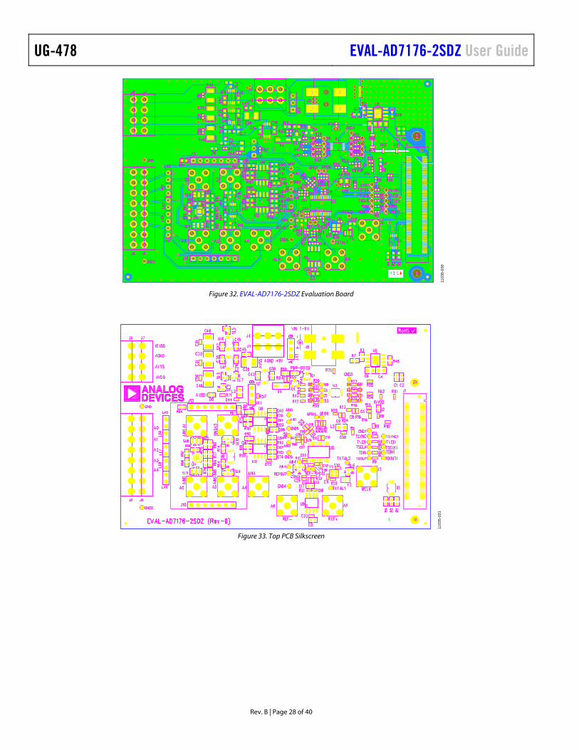
Figure 32. EVAL-AD7176-2SDZ Evaluation Board
1103
5-03
1
Figure 33. Top PCB Silkscreen
EVAL-AD7176-2SDZ User Guide UG-478
Rev. B | Page 29 of 40
1 103
5-03
2
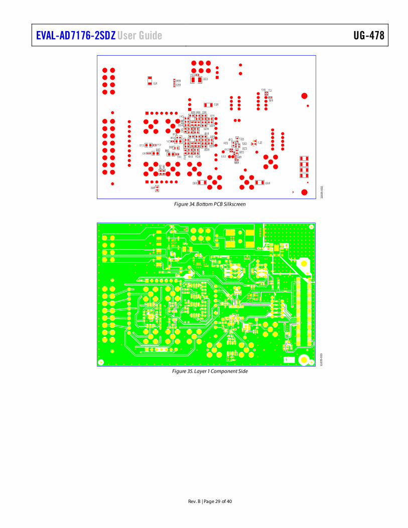
Figure 34. Bottom PCB Silkscreen
1103
5-03
3
Figure 35. Layer 1 Component Side
UG-478 EVAL-AD7176-2SDZ User Guide
Rev. B | Page 30 of 40
1103
5-03
4
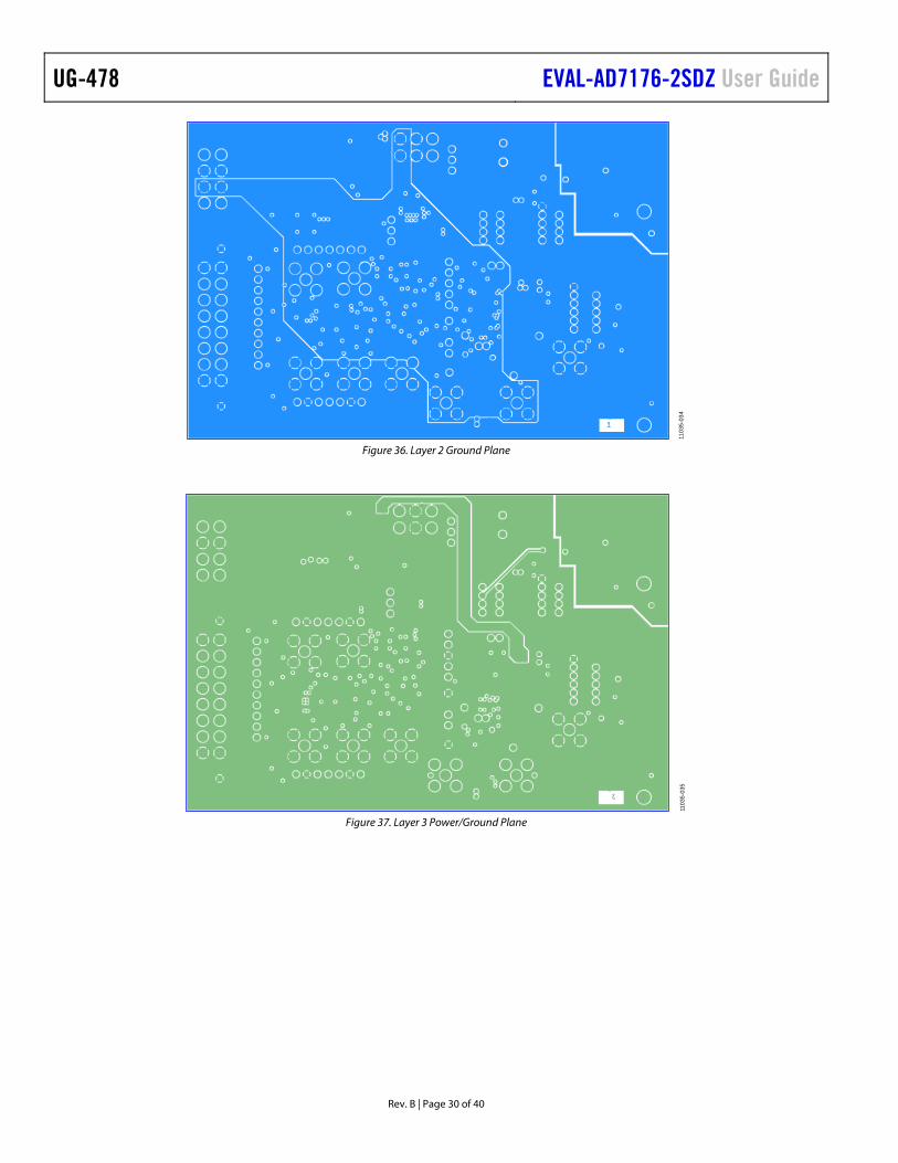
Figure 36. Layer 2 Ground Plane
1103
5-03
5
Figure 37. Layer 3 Power/Ground Plane
EVAL-AD7176-2SDZ User Guide UG-478
Rev. B | Page 31 of 40
1103
5-03
6
Figure 38. Layer 4 Component Side
UG-478 EVAL-AD7176-2SDZ User Guide
Rev. B | Page 32 of 40
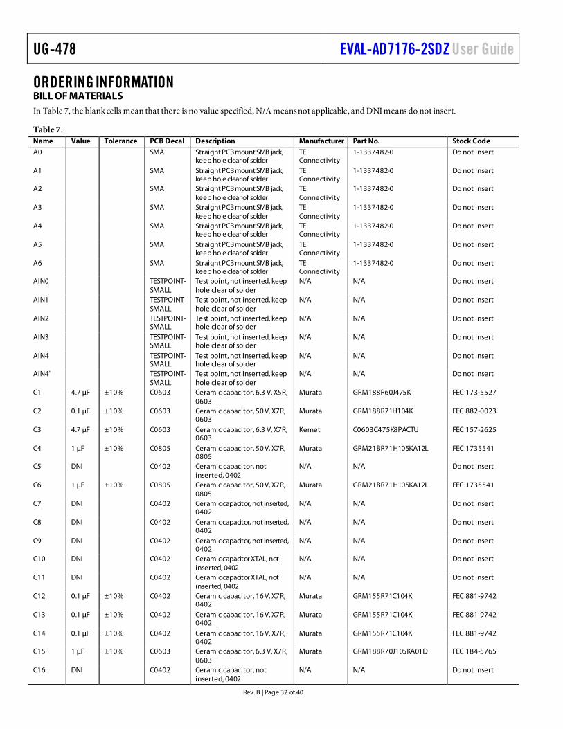
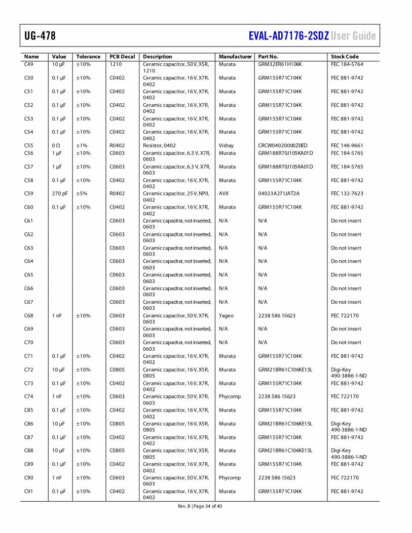
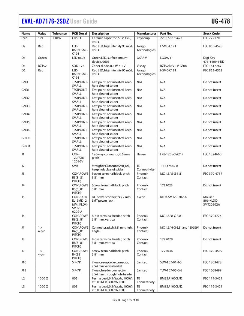
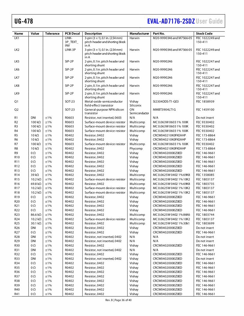
ORDERING INFORMATION BILL OF MATERIALS In Table 7, the blank cells mean that there is no value specified, N/A means not applicable, and DNI means do not insert.
Table 7. Name Value Tolerance PCB Decal Description Manufacturer Part No. Stock Code
A0 SMA Straight PCB mount SMB jack, keep hole clear of solder
TE Connectivity
1-1337482-0 Do not insert
A1 SMA Straight PCB mount SMB jack, keep hole clear of solder
TE Connectivity
1-1337482-0 Do not insert
A2 SMA Straight PCB mount SMB jack, keep hole clear of solder
TE Connectivity
1-1337482-0 Do not insert
A3 SMA Straight PCB mount SMB jack, keep hole clear of solder
TE Connectivity
1-1337482-0 Do not insert
A4 SMA Straight PCB mount SMB jack, keep hole clear of solder
TE Connectivity
1-1337482-0 Do not insert
A5 SMA Straight PCB mount SMB jack, keep hole clear of solder
TE Connectivity
1-1337482-0 Do not insert
A6 SMA Straight PCB mount SMB jack, keep hole clear of solder
TE Connectivity
1-1337482-0 Do not insert
AIN0 TESTPOINT-SMALL
Test point, not inserted, keep hole clear of solder
N/A N/A Do not insert
AIN1 TESTPOINT-SMALL
Test point, not inserted, keep hole clear of solder
N/A N/A Do not insert
AIN2 TESTPOINT-SMALL
Test point, not inserted, keep hole clear of solder
N/A N/A Do not insert
AIN3 TESTPOINT-SMALL
Test point, not inserted, keep hole clear of solder
N/A N/A Do not insert
AIN4 TESTPOINT-SMALL
Test point, not inserted, keep hole clear of solder
N/A N/A Do not insert
AIN4' TESTPOINT-SMALL
Test point, not inserted, keep hole clear of solder
N/A N/A Do not insert
C1 4.7 µF ±10% C0603 Ceramic capacitor, 6.3 V, X5R, 0603
Murata GRM188R60J475K FEC 173-5527
C2 0.1 µF ±10% C0603 Ceramic capacitor, 50 V, X7R, 0603
Murata GRM188R71H104K FEC 882-0023
C3 4.7 µF ±10% C0603 Ceramic capacitor, 6.3 V, X7R, 0603
Kemet C0603C475K8PACTU FEC 157-2625
C4 1 µF ±10% C0805 Ceramic capacitor, 50 V, X7R, 0805
Murata GRM21BR71H105KA12L FEC 1735541
C5 DNI C0402 Ceramic capacitor, not inserted, 0402
N/A N/A Do not insert
C6 1 µF ±10% C0805 Ceramic capacitor, 50 V, X7R, 0805
Murata GRM21BR71H105KA12L FEC 1735541
C7 DNI C0402 Ceramic capacitor, not inserted, 0402
N/A N/A Do not insert
C8 DNI C0402 Ceramic capacitor, not inserted, 0402
N/A N/A Do not insert
C9 DNI C0402 Ceramic capacitor, not inserted, 0402
N/A N/A Do not insert
C10 DNI C0402 Ceramic capacitor XTAL, not inserted, 0402
N/A N/A Do not insert
C11 DNI C0402 Ceramic capacitor XTAL, not inserted, 0402
N/A N/A Do not insert
C12 0.1 µF ±10% C0402 Ceramic capacitor, 16 V, X7R, 0402
Murata GRM155R71C104K FEC 881-9742
C13 0.1 µF ±10% C0402 Ceramic capacitor, 16 V, X7R, 0402
Murata GRM155R71C104K FEC 881-9742
C14 0.1 µF ±10% C0402 Ceramic capacitor, 16 V, X7R, 0402
Murata GRM155R71C104K FEC 881-9742
C15 1 µF ±10% C0603 Ceramic capacitor, 6.3 V, X7R, 0603
Murata GRM188R70J105KA01D FEC 184-5765
C16 DNI C0402 Ceramic capacitor, not inserted, 0402
N/A N/A Do not insert
EVAL-AD7176-2SDZ User Guide UG-478
Rev. B | Page 33 of 40
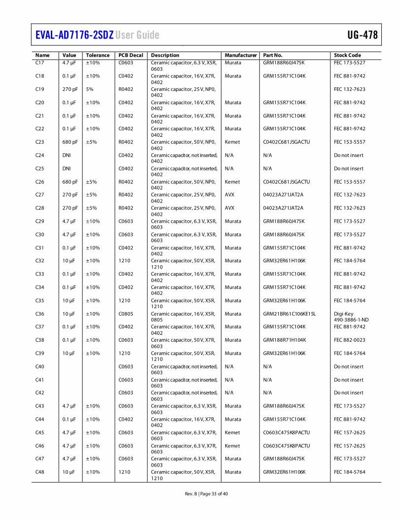
Name Value Tolerance PCB Decal Description Manufacturer Part No. Stock Code C17 4.7 µF ±10% C0603 Ceramic capacitor, 6.3 V, X5R,
0603 Murata GRM188R60J475K FEC 173-5527
C18 0.1 µF ±10% C0402 Ceramic capacitor, 16 V, X7R, 0402
Murata GRM155R71C104K FEC 881-9742
C19 270 pF 5% R0402 Ceramic capacitor, 25 V, NP0, 0402
FEC 132-7623
C20 0.1 µF ±10% C0402 Ceramic capacitor, 16 V, X7R, 0402
Murata GRM155R71C104K FEC 881-9742
C21 0.1 µF ±10% C0402 Ceramic capacitor, 16 V, X7R, 0402
Murata GRM155R71C104K FEC 881-9742
C22 0.1 µF ±10% C0402 Ceramic capacitor, 16 V, X7R, 0402
Murata GRM155R71C104K FEC 881-9742
C23 680 pF ±5% R0402 Ceramic capacitor, 50 V, NP0, 0402
Kemet C0402C681J5GACTU FEC 153-5557
C24 DNI C0402 Ceramic capacitor, not inserted, 0402
N/A N/A Do not insert
C25 DNI C0402 Ceramic capacitor, not inserted, 0402
N/A N/A Do not insert
C26 680 pF ±5% R0402 Ceramic capacitor, 50 V, NP0, 0402
Kemet C0402C681J5GACTU FEC 153-5557
C27 270 pF ±5% R0402 Ceramic capacitor, 25 V, NP0, 0402
AVX 04023A271JAT2A FEC 132-7623
C28 270 pF ±5% R0402 Ceramic capacitor, 25 V, NP0, 0402
AVX 04023A271JAT2A FEC 132-7623
C29 4.7 µF ±10% C0603 Ceramic capacitor, 6.3 V, X5R, 0603
Murata GRM188R60J475K FEC 173-5527
C30 4.7 µF ±10% C0603 Ceramic capacitor, 6.3 V, X5R, 0603
Murata GRM188R60J475K FEC 173-5527
C31 0.1 µF ±10% C0402 Ceramic capacitor, 16 V, X7R, 0402
Murata GRM155R71C104K FEC 881-9742
C32 10 µF ±10% 1210 Ceramic capacitor, 50 V, X5R, 1210
Murata GRM32ER61H106K FEC 184-5764
C33 0.1 µF ±10% C0402 Ceramic capacitor, 16 V, X7R, 0402
Murata GRM155R71C104K FEC 881-9742
C34 0.1 µF ±10% C0402 Ceramic capacitor, 16 V, X7R, 0402
Murata GRM155R71C104K FEC 881-9742
C35 10 µF ±10% 1210 Ceramic capacitor, 50 V, X5R, 1210
Murata GRM32ER61H106K FEC 184-5764
C36 10 µF ±10% C0805 Ceramic capacitor, 16 V, X5R, 0805
Murata GRM21BR61C106KE15L Digi-Key 490-3886-1-ND
C37 0.1 µF ±10% C0402 Ceramic capacitor, 16 V, X7R, 0402
Murata GRM155R71C104K FEC 881-9742
C38 0.1 µF ±10% C0603 Ceramic capacitor, 50 V, X7R, 0603
Murata GRM188R71H104K FEC 882-0023
C39 10 µF ±10% 1210 Ceramic capacitor, 50 V, X5R, 1210
Murata GRM32ER61H106K FEC 184-5764
C40 C0603 Ceramic capacitor, not inserted, 0603
N/A N/A Do not insert
C41 C0603 Ceramic capacitor, not inserted, 0603
N/A N/A Do not insert
C42 C0603 Ceramic capacitor, not inserted, 0603
N/A N/A Do not insert
C43 4.7 µF ±10% C0603 Ceramic capacitor, 6.3 V, X5R, 0603
Murata GRM188R60J475K FEC 173-5527
C44 0.1 µF ±10% C0402 Ceramic capacitor, 16 V, X7R, 0402
Murata GRM155R71C104K FEC 881-9742
C45 4.7 µF ±10% C0603 Ceramic capacitor, 6.3 V, X7R, 0603
Kemet C0603C475K8PACTU FEC 157-2625
C46 4.7 µF ±10% C0603 Ceramic capacitor, 6.3 V, X7R, 0603
Kemet C0603C475K8PACTU FEC 157-2625
C47 4.7 µF ±10% C0603 Ceramic capacitor, 6.3 V, X5R, 0603
Murata GRM188R60J475K FEC 173-5527
C48 10 µF ±10% 1210 Ceramic capacitor, 50 V, X5R, 1210
Murata GRM32ER61H106K FEC 184-5764
UG-478 EVAL-AD7176-2SDZ User Guide
Rev. B | Page 34 of 40
Name Value Tolerance PCB Decal Description Manufacturer Part No. Stock Code C49 10 µF ±10% 1210 Ceramic capacitor, 50 V, X5R,
1210 Murata GRM32ER61H106K FEC 184-5764
C50 0.1 µF ±10% C0402 Ceramic capacitor, 16 V, X7R, 0402
Murata GRM155R71C104K FEC 881-9742
C51 0.1 µF ±10% C0402 Ceramic capacitor, 16 V, X7R, 0402
Murata GRM155R71C104K FEC 881-9742
C52 0.1 µF ±10% C0402 Ceramic capacitor, 16 V, X7R, 0402
Murata GRM155R71C104K FEC 881-9742
C53 0.1 µF ±10% C0402 Ceramic capacitor, 16 V, X7R, 0402
Murata GRM155R71C104K FEC 881-9742
C54 0.1 µF ±10% C0402 Ceramic capacitor, 16 V, X7R, 0402
Murata GRM155R71C104K FEC 881-9742
C55 0 Ω ±1% R0402 Resistor, 0402 Vishay CRCW04020000Z0ED FEC 146-9661 C56 1 µF ±10% C0603 Ceramic capacitor, 6.3 V, X7R,
0603 Murata GRM188R70J105KA01D FEC 184-5765
C57 1 µF ±10% C0603 Ceramic capacitor, 6.3 V, X7R, 0603
Murata GRM188R70J105KA01D FEC 184-5765
C58 0.1 µF ±10% C0402 Ceramic capacitor, 16 V, X7R, 0402
Murata GRM155R71C104K FEC 881-9742
C59 270 pF ±5% R0402 Ceramic capacitor, 25 V, NP0, 0402
AVX 04023A271JAT2A FEC 132-7623
C60 0.1 µF ±10% C0402 Ceramic capacitor, 16 V, X7R, 0402
Murata GRM155R71C104K FEC 881-9742
C61 C0603 Ceramic capacitor, not inserted, 0603
N/A N/A Do not insert
C62 C0603 Ceramic capacitor, not inserted, 0603
N/A N/A Do not insert
C63 C0603 Ceramic capacitor, not inserted, 0603
N/A N/A Do not insert
C64 C0603 Ceramic capacitor, not inserted, 0603
N/A N/A Do not insert
C65 C0603 Ceramic capacitor, not inserted, 0603
N/A N/A Do not insert
C66 C0603 Ceramic capacitor, not inserted, 0603
N/A N/A Do not insert
C67 C0603 Ceramic capacitor, not inserted, 0603
N/A N/A Do not insert
C68 1 nF ±10% C0603 Ceramic capacitor, 50 V, X7R, 0603
Yageo 2238 586 15623 FEC 722170
C69 C0603 Ceramic capacitor, not inserted, 0603
N/A N/A Do not insert
C70 C0603 Ceramic capacitor, not inserted, 0603
N/A N/A Do not insert
C71 0.1 µF ±10% C0402 Ceramic capacitor, 16 V, X7R, 0402
Murata GRM155R71C104K FEC 881-9742
C72 10 µF ±10% C0805 Ceramic capacitor, 16 V, X5R, 0805
Murata GRM21BR61C106KE15L Digi-Key 490-3886-1-ND
C73 0.1 µF ±10% C0402 Ceramic capacitor, 16 V, X7R, 0402
Murata GRM155R71C104K FEC 881-9742
C74 1 nF ±10% C0603 Ceramic capacitor, 50 V, X7R, 0603
Phycomp 2238 586 15623 FEC 722170
C85 0.1 µF ±10% C0402 Ceramic capacitor, 16 V, X7R, 0402
Murata GRM155R71C104K FEC 881-9742
C86 10 µF ±10% C0805 Ceramic capacitor, 16 V, X5R, 0805
Murata GRM21BR61C106KE15L Digi-Key 490-3886-1-ND
C87 0.1 µF ±10% C0402 Ceramic capacitor, 16 V, X7R, 0402
Murata GRM155R71C104K FEC 881-9742
C88 10 µF ±10% C0805 Ceramic capacitor, 16 V, X5R, 0805
Murata GRM21BR61C106KE15L Digi-Key 490-3886-1-ND
C89 0.1 µF ±10% C0402 Ceramic capacitor, 16 V, X7R, 0402
Murata GRM155R71C104K FEC 881-9742
C90 1 nF ±10% C0603 Ceramic capacitor, 50 V, X7R, 0603
Phycomp 2238 586 15623 FEC 722170
C91 0.1 µF ±10% C0402 Ceramic capacitor, 16 V, X7R, 0402
Murata GRM155R71C104K FEC 881-9742
EVAL-AD7176-2SDZ User Guide UG-478
Rev. B | Page 35 of 40
Name Value Tolerance PCB Decal Description Manufacturer Part No. Stock Code C92 1 nF ±10% C0603 Ceramic capacitor, 50 V, X7R,
0603 Phycomp 2238 586 15623 FEC 722170
D2 Red LED-0603HSML-C191
Red LED, high intensity 90 mCd, 0603
Avago Technologies
HSMC-C191 FEC 855-4528
D4 Green LED-0603 Green LED, surface-mount device, 0603
OSRAM LGQ971 Digi-Key 475-1409-1-ND
D5 BZT52 SOD-123 Zener diode, 0.5 W, 5.1 V Vishay BZT52B5V1-V-GS08 FEC 1617767 D6 Red LED-
0603HSML-C191
Red LED, high intensity 90 mCd, 0603
Avago Technologies
HSMC-C191 FEC 855-4528
GND TESTPOINT-SMALL
Test point, not inserted, keep hole clear of solder
N/A N/A Do not insert
GND1 TESTPOINT-SMALL
Test point, not inserted, keep hole clear of solder
N/A N/A Do not insert
GND2 TESTPOINT-SMALL
Test point, not inserted, keep hole clear of solder
N/A N/A Do not insert
GND3 TESTPOINT-SMALL
Test point, not inserted, keep hole clear of solder
N/A N/A Do not insert
GND4 TESTPOINT-SMALL
Test point, not inserted, keep hole clear of solder
N/A N/A Do not insert
GND5 TESTPOINT-SMALL
Test point, not inserted, keep hole clear of solder
N/A N/A Do not insert
GND6 TESTPOINT-SMALL
Test point, not inserted, keep hole clear of solder
N/A N/A Do not insert
GPIO0 TESTPOINT-SMALL
Test point, not inserted, keep hole clear of solder
N/A N/A Do not insert
GPIO1 TESTPOINT-SMALL
Test point, not inserted, keep hole clear of solder
N/A N/A Do not insert
J1 CON-120/FX8-120S-SV
120-way connector, 0.6 mm pitch
Hirose FX8-120S-SV(21) FEC 1324660
J2 SMB Straight PCB mount SMB jack, keep hole clear of solder
TE Connectivity
1-1337482-0 Do not insert
J3 CON\POWER3(3_81 PITCH)
Socket terminal block, pitch 3.81 mm
Phoenix Contact
MC 1,5/ 5-G-3,81 FEC 370-4737
J4 CON\POWER3(3_81 PITCH)
Screw terminal block, pitch 3.81 mm
Phoenix Contact
1727023 Do not insert
J5 CON\BARREL_SMD_2MM_KLDX-SMT2-0202-A
DC power connectors, 2 mm SMT power jack
Kycon KLDX-SMT2-0202-A Mouser 806-KLDX-SMT20202A
J6 CON\POWER8(3_81 PITCH)
8-pin terminal header, pitch 3.81 mm, vertical
Phoenix Contact
MC 1,5/ 8-G-3,81 FEC 3704774
J7 1 × 4-pin
CON\POWER4(3_81 PITCH)
Connector, pitch 3.81 mm, right angle
Phoenix Contact
MC 1,5/ 4-G-3,81 and 180-3594 Do not insert
J8 CON\POWER8(3_81 PITCH)
8-pin terminal header, pitch 3.81 mm, vertical
Phoenix Contact
1727078 Do not insert
J9 1 × 4-pin
CON\POWER4(381 PITCH)
Screw terminal block, pitch 3.81 mm
Phoenix Contact
1727036 FEC 370-4592
J10 SIP-7P 7-way, receptacle connector, 2.54 mm vertical socket
Samtec SSW-107-01-T-S FEC 1803478
J13 SIP-7P 7-way, header connector, 2.54 mm through hole header
Samtec TLW-107-05-G-S FEC 1668499
L2 1000 Ω 805 Ferrite bead, 0.3 Ω at dc, 1000 Ω at 100 MHz, 350 mA, 0805
TE Connectivity
BMB2A1000LN2 FEC 119-3421
L3 1000 Ω 805 Ferrite bead, 0.3 Ω at dc, 1000 Ω at 100 MHz, 350 mA, 0805
TE Connectivity
BMB2A1000LN2 FEC 119-3421
UG-478 EVAL-AD7176-2SDZ User Guide
Rev. B | Page 36 of 40
Name Value Tolerance PCB Decal Description Manufacturer Part No. Stock Code LK1 LINK-
3P_TEXT_ INV
3-pin (3 × 1), 0.1 in. (2.54 mm) pitch header and shorting block in A
Harwin M20-9990346 and M7566-05 FEC 1022249 and 150-411
LK2 LINK-3P 3-pin (3 × 1), 0.1 in. (2.54 mm) pitch header and shorting block in A
Harwin M20-9990346 and M7566-05 FEC 1022249 and 150-411
LK5 SIP-2P 2-pin, 0.1in. pitch header and shorting shunt
Harwin M20-9990246 FEC 1022247 and 150-411
LK6 SIP-2P 2-pin, 0.1in. pitch header and shorting shunt
Harwin M20-9990246 FEC 1022247 and 150-411
LK7 SIP-2P 2-pin, 0.1in. pitch header and shorting shunt
Harwin M20-9990246 FEC 1022247 and 150-411
LK8 SIP-2P 2-pin, 0.1in. pitch header and shorting shunt
Harwin M20-9990246 FEC 1022247 and 150-411
LK9 SIP-2P 2-pin, 0.1in. pitch header and shorting shunt
Harwin M20-9990246 FEC 1022247 and 150-411
Q1 SOT-23 Metal-oxide-semiconductor field-effect transistor
Vishay Siliconix
SI2304DDS-T1-GE3 FEC 1858939
Q2 SOT-23 General-purpose NPN silicon transistor
ON Semiconductor
MMBT3904LT1G FEC 1459100
R1 DNI ±1% R0603 Resistor, not inserted, 0603 N/A N/A Do not insert R2 100 kΩ ±1% R0603 Surface-mount device resistor Multicomp MC 0.063W 0603 1% 100K FEC 9330402 R3 100 kΩ ±1% R0603 Surface-mount device resistor Multicomp MC 0.063W 0603 1% 100K FEC 9330402 R4 100 kΩ ±1% R0603 Surface-mount device resistor Multicomp MC 0.063W 0603 1% 100K FEC 9330402 R5 10 kΩ ±1% R0402 Resistor, 0402 Vishay CRCW040210K0FKEAHP FEC 173-8864 R6 10 kΩ ±1% R0402 Resistor, 0402 Vishay CRCW040210K0FKEAHP FEC 173-8864 R7 100 kΩ ±1% R0603 Surface-mount device resistor Multicomp MC 0.063W 0603 1% 100K FEC 9330402 R8 10 kΩ ±1% R0402 Resistor, 0402 Phycomp CRCW040210K0FKEAHP FEC 173-8864 R9 0 Ω ±1% R0402 Resistor, 0402 Vishay CRCW04020000Z0ED FEC 146-9661 R10 0 Ω ±1% R0402 Resistor, 0402 Vishay CRCW04020000Z0ED FEC 146-9661 R11 0 Ω ±1% R0402 Resistor, 0402 Vishay CRCW04020000Z0ED FEC 146-9661 R12 0 Ω ±1% R0402 Resistor, 0402 Vishay CRCW04020000Z0ED FEC 146-9661 R13 0 Ω ±1% R0402 Resistor, 0402 Vishay CRCW04020000Z0ED FEC 146-9661 R14 39 kΩ ±1% R0402 Resistor, 0402 Multicomp MC 0.0625W 0402 1% 69K8 FEC 1358085 R15 10.2 kΩ ±1% R0402 Surface-mount device resistor Multicomp MC 0.0625W 0402 1% 10K2 FEC 1803137 R16 69.8 kΩ ±1% R0402 Resistor, 0402 Multicomp MC 0.0625W 0402 1% 69K8 FEC 1803735 R17 10.2 kΩ ±1% R0402 Surface-mount device resistor Multicomp MC 0.0625W 0402 1% 10K2 FEC 1803137 R18 10.2 kΩ ±1% R0402 Surface-mount device resistor Multicomp MC 0.0625W 0402 1% 10K2 FEC 1803137 R19 0 Ω ±1% R0402 Resistor, 0402 Vishay CRCW04020000Z0ED FEC 146-9661 R20 0 Ω ±1% R0402 Resistor, 0402 Vishay CRCW04020000Z0ED FEC 146-9661 R21 0 Ω ±1% R0402 Resistor, 0402 Vishay CRCW04020000Z0ED FEC 146-9661 R22 0 Ω ±1% R0402 Resistor, 0402 Vishay CRCW04020000Z0ED FEC 146-9661 R23 86.6 kΩ ±1% R0402 Resistor, 0402 Multicomp MC 0.0625W 0402 1% 86K6 FEC 1803744 R24 10.2 kΩ ±1% R0402 Surface-mount device resistor Multicomp MC 0.0625W 0402 1% 10K2 FEC 1803137 R25 30.1 kΩ ±1% R0402 Resistor, 0402 Multicomp MC 0.0625W 0402 1% 30k1 FEC 1803699 R26 DNI ±1% R0402 Resistor, 0402 Vishay CRCW04020000Z0ED Do not insert R27 0 Ω ±1% R0402 Resistor, 0402 Vishay CRCW04020000Z0ED FEC 146-9661 R28 DNI ±1% R0402 Resistor, not inserted, 0402 N/A N/A Do not insert R29 DNI ±1% R0402 Resistor, not inserted, 0402 N/A N/A Do not insert R30 0 Ω ±1% R0402 Resistor, 0402 Vishay CRCW04020000Z0ED FEC 146-9661 R31 DNI ±1% R0402 Resistor, not inserted, 0402 N/A N/A Do not insert R32 0 Ω ±1% R0402 Resistor, 0402 Vishay CRCW04020000Z0ED FEC 146-9661 R33 DNI ±1% R0402 Resistor, not inserted, 0402 Vishay CRCW04020000Z0ED Do not insert R34 0 Ω ±1% R0402 Resistor, 0402 Vishay CRCW04020000Z0ED FEC 146-9661 R35 0 Ω ±1% R0402 Resistor, 0402 Vishay CRCW04020000Z0ED FEC 146-9661 R36 0 Ω ±1% R0402 Resistor, 0402 Vishay CRCW04020000Z0ED FEC 146-9661 R37 0 Ω ±1% R0402 Resistor, 0402 Vishay CRCW04020000Z0ED FEC 146-9661 R38 0 Ω ±1% R0402 Resistor, 0402 Vishay CRCW04020000Z0ED FEC 146-9661 R39 0 Ω ±1% R0402 Resistor, 0402 Vishay CRCW04020000Z0ED FEC 146-9661 R40 0 Ω ±1% R0402 Resistor, 0402 Vishay CRCW04020000Z0ED FEC 146-9661 R41 0 Ω ±1% R0402 Resistor, 0402 Vishay CRCW04020000Z0ED FEC 146-9661
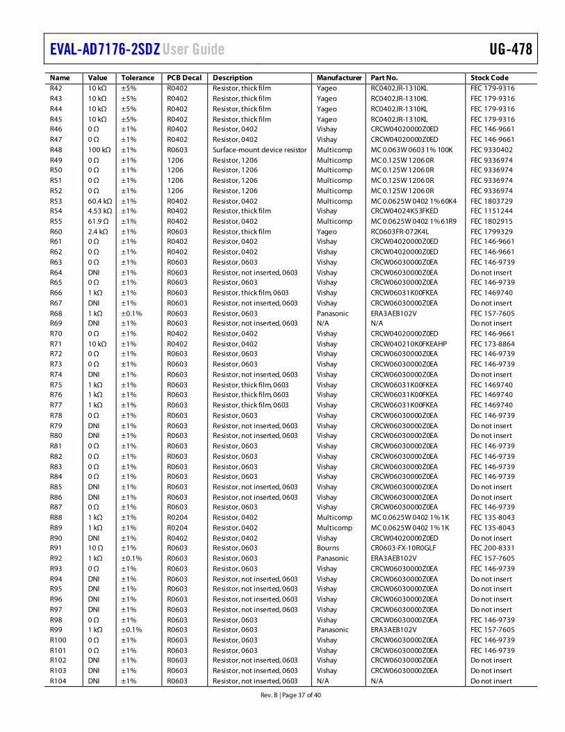
EVAL-AD7176-2SDZ User Guide UG-478
Rev. B | Page 37 of 40
Name Value Tolerance PCB Decal Description Manufacturer Part No. Stock Code R42 10 kΩ ±5% R0402 Resistor, thick film Yageo RC0402JR-1310KL FEC 179-9316 R43 10 kΩ ±5% R0402 Resistor, thick film Yageo RC0402JR-1310KL FEC 179-9316 R44 10 kΩ ±5% R0402 Resistor, thick film Yageo RC0402JR-1310KL FEC 179-9316 R45 10 kΩ ±5% R0402 Resistor, thick film Yageo RC0402JR-1310KL FEC 179-9316 R46 0 Ω ±1% R0402 Resistor, 0402 Vishay CRCW04020000Z0ED FEC 146-9661 R47 0 Ω ±1% R0402 Resistor, 0402 Vishay CRCW04020000Z0ED FEC 146-9661 R48 100 kΩ ±1% R0603 Surface-mount device resistor Multicomp MC 0.063W 0603 1% 100K FEC 9330402 R49 0 Ω ±1% 1206 Resistor, 1206 Multicomp MC 0.125W 1206 0R FEC 9336974 R50 0 Ω ±1% 1206 Resistor, 1206 Multicomp MC 0.125W 1206 0R FEC 9336974 R51 0 Ω ±1% 1206 Resistor, 1206 Multicomp MC 0.125W 1206 0R FEC 9336974 R52 0 Ω ±1% 1206 Resistor, 1206 Multicomp MC 0.125W 1206 0R FEC 9336974 R53 60.4 kΩ ±1% R0402 Resistor, 0402 Multicomp MC 0.0625W 0402 1% 60K4 FEC 1803729 R54 4.53 kΩ ±1% R0402 Resistor, thick film Vishay CRCW04024K53FKED FEC 1151244 R55 61.9 Ω ±1% R0402 Resistor, 0402 Multicomp MC 0.0625W 0402 1% 61R9 FEC 1802915 R60 2.4 kΩ ±1% R0603 Resistor, thick film Yageo RC0603FR-072K4L FEC 1799329 R61 0 Ω ±1% R0402 Resistor, 0402 Vishay CRCW04020000Z0ED FEC 146-9661 R62 0 Ω ±1% R0402 Resistor, 0402 Vishay CRCW04020000Z0ED FEC 146-9661 R63 0 Ω ±1% R0603 Resistor, 0603 Vishay CRCW06030000Z0EA FEC 146-9739 R64 DNI ±1% R0603 Resistor, not inserted, 0603 Vishay CRCW06030000Z0EA Do not insert R65 0 Ω ±1% R0603 Resistor, 0603 Vishay CRCW06030000Z0EA FEC 146-9739 R66 1 kΩ ±1% R0603 Resistor, thick film, 0603 Vishay CRCW06031K00FKEA FEC 1469740 R67 DNI ±1% R0603 Resistor, not inserted, 0603 Vishay CRCW06030000Z0EA Do not insert R68 1 kΩ ±0.1% R0603 Resistor, 0603 Panasonic ERA3AEB102V FEC 157-7605 R69 DNI ±1% R0603 Resistor, not inserted, 0603 N/A N/A Do not insert R70 0 Ω ±1% R0402 Resistor, 0402 Vishay CRCW04020000Z0ED FEC 146-9661 R71 10 kΩ ±1% R0402 Resistor, 0402 Vishay CRCW040210K0FKEAHP FEC 173-8864 R72 0 Ω ±1% R0603 Resistor, 0603 Vishay CRCW06030000Z0EA FEC 146-9739 R73 0 Ω ±1% R0603 Resistor, 0603 Vishay CRCW06030000Z0EA FEC 146-9739 R74 DNI ±1% R0603 Resistor, not inserted, 0603 Vishay CRCW06030000Z0EA Do not insert R75 1 kΩ ±1% R0603 Resistor, thick film, 0603 Vishay CRCW06031K00FKEA FEC 1469740 R76 1 kΩ ±1% R0603 Resistor, thick film, 0603 Vishay CRCW06031K00FKEA FEC 1469740 R77 1 kΩ ±1% R0603 Resistor, thick film, 0603 Vishay CRCW06031K00FKEA FEC 1469740 R78 0 Ω ±1% R0603 Resistor, 0603 Vishay CRCW06030000Z0EA FEC 146-9739 R79 DNI ±1% R0603 Resistor, not inserted, 0603 Vishay CRCW06030000Z0EA Do not insert R80 DNI ±1% R0603 Resistor, not inserted, 0603 Vishay CRCW06030000Z0EA Do not insert R81 0 Ω ±1% R0603 Resistor, 0603 Vishay CRCW06030000Z0EA FEC 146-9739 R82 0 Ω ±1% R0603 Resistor, 0603 Vishay CRCW06030000Z0EA FEC 146-9739 R83 0 Ω ±1% R0603 Resistor, 0603 Vishay CRCW06030000Z0EA FEC 146-9739 R84 0 Ω ±1% R0603 Resistor, 0603 Vishay CRCW06030000Z0EA FEC 146-9739 R85 DNI ±1% R0603 Resistor, not inserted, 0603 Vishay CRCW06030000Z0EA Do not insert R86 DNI ±1% R0603 Resistor, not inserted, 0603 Vishay CRCW06030000Z0EA Do not insert R87 0 Ω ±1% R0603 Resistor, 0603 Vishay CRCW06030000Z0EA FEC 146-9739 R88 1 kΩ ±1% R0204 Resistor, 0402 Multicomp MC 0.0625W 0402 1% 1K FEC 135-8043 R89 1 kΩ ±1% R0204 Resistor, 0402 Multicomp MC 0.0625W 0402 1% 1K FEC 135-8043 R90 DNI ±1% R0402 Resistor, 0402 Vishay CRCW04020000Z0ED Do not insert R91 10 Ω ±1% R0603 Resistor, 0603 Bourns CR0603-FX-10R0GLF FEC 200-8331 R92 1 kΩ ±0.1% R0603 Resistor, 0603 Panasonic ERA3AEB102V FEC 157-7605 R93 0 Ω ±1% R0603 Resistor, 0603 Vishay CRCW06030000Z0EA FEC 146-9739 R94 DNI ±1% R0603 Resistor, not inserted, 0603 Vishay CRCW06030000Z0EA Do not insert R95 DNI ±1% R0603 Resistor, not inserted, 0603 Vishay CRCW06030000Z0EA Do not insert R96 DNI ±1% R0603 Resistor, not inserted, 0603 Vishay CRCW06030000Z0EA Do not insert R97 DNI ±1% R0603 Resistor, not inserted, 0603 Vishay CRCW06030000Z0EA Do not insert R98 0 Ω ±1% R0603 Resistor, 0603 Vishay CRCW06030000Z0EA FEC 146-9739 R99 1 kΩ ±0.1% R0603 Resistor, 0603 Panasonic ERA3AEB102V FEC 157-7605 R100 0 Ω ±1% R0603 Resistor, 0603 Vishay CRCW06030000Z0EA FEC 146-9739 R101 0 Ω ±1% R0603 Resistor, 0603 Vishay CRCW06030000Z0EA FEC 146-9739 R102 DNI ±1% R0603 Resistor, not inserted, 0603 Vishay CRCW06030000Z0EA Do not insert R103 DNI ±1% R0603 Resistor, not inserted, 0603 Vishay CRCW06030000Z0EA Do not insert R104 DNI ±1% R0603 Resistor, not inserted, 0603 N/A N/A Do not insert
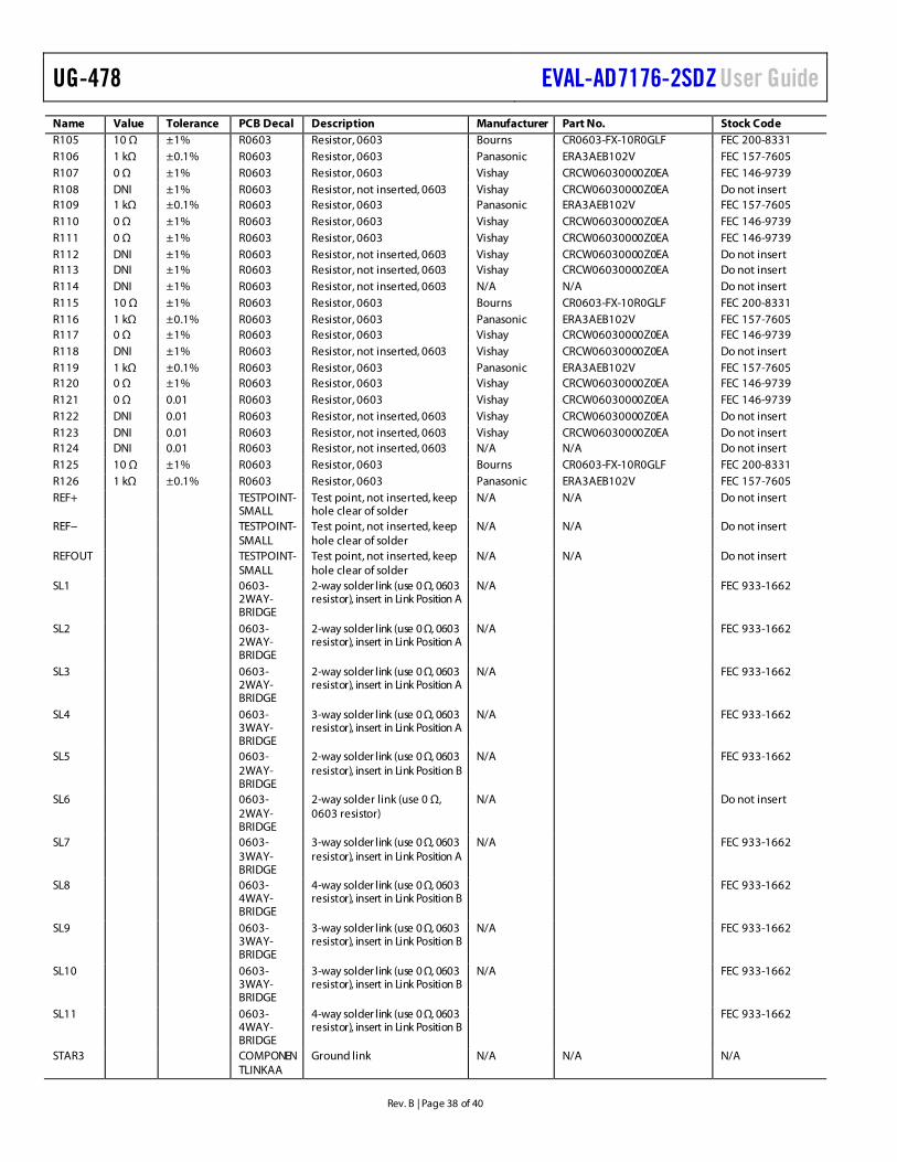
UG-478 EVAL-AD7176-2SDZ User Guide
Rev. B | Page 38 of 40
Name Value Tolerance PCB Decal Description Manufacturer Part No. Stock Code R105 10 Ω ±1% R0603 Resistor, 0603 Bourns CR0603-FX-10R0GLF FEC 200-8331 R106 1 kΩ ±0.1% R0603 Resistor, 0603 Panasonic ERA3AEB102V FEC 157-7605 R107 0 Ω ±1% R0603 Resistor, 0603 Vishay CRCW06030000Z0EA FEC 146-9739 R108 DNI ±1% R0603 Resistor, not inserted, 0603 Vishay CRCW06030000Z0EA Do not insert R109 1 kΩ ±0.1% R0603 Resistor, 0603 Panasonic ERA3AEB102V FEC 157-7605 R110 0 Ω ±1% R0603 Resistor, 0603 Vishay CRCW06030000Z0EA FEC 146-9739 R111 0 Ω ±1% R0603 Resistor, 0603 Vishay CRCW06030000Z0EA FEC 146-9739 R112 DNI ±1% R0603 Resistor, not inserted, 0603 Vishay CRCW06030000Z0EA Do not insert R113 DNI ±1% R0603 Resistor, not inserted, 0603 Vishay CRCW06030000Z0EA Do not insert R114 DNI ±1% R0603 Resistor, not inserted, 0603 N/A N/A Do not insert R115 10 Ω ±1% R0603 Resistor, 0603 Bourns CR0603-FX-10R0GLF FEC 200-8331 R116 1 kΩ ±0.1% R0603 Resistor, 0603 Panasonic ERA3AEB102V FEC 157-7605 R117 0 Ω ±1% R0603 Resistor, 0603 Vishay CRCW06030000Z0EA FEC 146-9739 R118 DNI ±1% R0603 Resistor, not inserted, 0603 Vishay CRCW06030000Z0EA Do not insert R119 1 kΩ ±0.1% R0603 Resistor, 0603 Panasonic ERA3AEB102V FEC 157-7605 R120 0 Ω ±1% R0603 Resistor, 0603 Vishay CRCW06030000Z0EA FEC 146-9739 R121 0 Ω 0.01 R0603 Resistor, 0603 Vishay CRCW06030000Z0EA FEC 146-9739 R122 DNI 0.01 R0603 Resistor, not inserted, 0603 Vishay CRCW06030000Z0EA Do not insert R123 DNI 0.01 R0603 Resistor, not inserted, 0603 Vishay CRCW06030000Z0EA Do not insert R124 DNI 0.01 R0603 Resistor, not inserted, 0603 N/A N/A Do not insert R125 10 Ω ±1% R0603 Resistor, 0603 Bourns CR0603-FX-10R0GLF FEC 200-8331 R126 1 kΩ ±0.1% R0603 Resistor, 0603 Panasonic ERA3AEB102V FEC 157-7605 REF+ TESTPOINT-
SMALL Test point, not inserted, keep hole clear of solder
N/A N/A Do not insert
REF− TESTPOINT-SMALL
Test point, not inserted, keep hole clear of solder
N/A N/A Do not insert
REFOUT TESTPOINT-SMALL
Test point, not inserted, keep hole clear of solder
N/A N/A Do not insert
SL1 0603-2WAY-BRIDGE
2-way solder link (use 0 Ω, 0603 resistor), insert in Link Position A
N/A FEC 933-1662
SL2 0603-2WAY-BRIDGE
2-way solder link (use 0 Ω, 0603 resistor), insert in Link Position A
N/A FEC 933-1662
SL3 0603-2WAY-BRIDGE
2-way solder link (use 0 Ω, 0603 resistor), insert in Link Position A
N/A FEC 933-1662
SL4 0603-3WAY-BRIDGE
3-way solder link (use 0 Ω, 0603 resistor), insert in Link Position A
N/A FEC 933-1662
SL5 0603-2WAY-BRIDGE
2-way solder link (use 0 Ω, 0603 resistor), insert in Link Position B
N/A FEC 933-1662
SL6 0603-2WAY-BRIDGE
2-way solder link (use 0 Ω, 0603 resistor)
N/A Do not insert
SL7 0603-3WAY-BRIDGE
3-way solder link (use 0 Ω, 0603 resistor), insert in Link Position A
N/A FEC 933-1662
SL8 0603-4WAY-BRIDGE
4-way solder link (use 0 Ω, 0603 resistor), insert in Link Position B
FEC 933-1662
SL9 0603-3WAY-BRIDGE
3-way solder link (use 0 Ω, 0603 resistor), insert in Link Position B
N/A FEC 933-1662
SL10 0603-3WAY-BRIDGE
3-way solder link (use 0 Ω, 0603 resistor), insert in Link Position B
N/A FEC 933-1662
SL11 0603-4WAY-BRIDGE
4-way solder link (use 0 Ω, 0603 resistor), insert in Link Position B
FEC 933-1662
STAR3 COMPONENTLINKAA
Ground link N/A N/A N/A
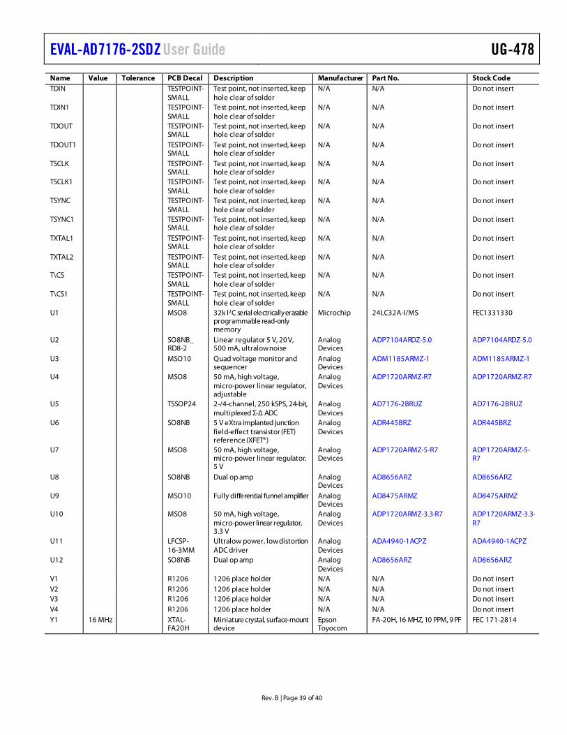
EVAL-AD7176-2SDZ User Guide UG-478
Rev. B | Page 39 of 40
Name Value Tolerance PCB Decal Description Manufacturer Part No. Stock Code TDIN TESTPOINT-
SMALL Test point, not inserted, keep hole clear of solder
N/A N/A Do not insert
TDIN1 TESTPOINT-SMALL
Test point, not inserted, keep hole clear of solder
N/A N/A Do not insert
TDOUT TESTPOINT-SMALL
Test point, not inserted, keep hole clear of solder
N/A N/A Do not insert
TDOUT1 TESTPOINT-SMALL
Test point, not inserted, keep hole clear of solder
N/A N/A Do not insert
TSCLK TESTPOINT-SMALL
Test point, not inserted, keep hole clear of solder
N/A N/A Do not insert
TSCLK1 TESTPOINT-SMALL
Test point, not inserted, keep hole clear of solder
N/A N/A Do not insert
TSYNC TESTPOINT-SMALL
Test point, not inserted, keep hole clear of solder
N/A N/A Do not insert
TSYNC1 TESTPOINT-SMALL
Test point, not inserted, keep hole clear of solder
N/A N/A Do not insert
TXTAL1 TESTPOINT-SMALL
Test point, not inserted, keep hole clear of solder
N/A N/A Do not insert
TXTAL2 TESTPOINT-SMALL
Test point, not inserted, keep hole clear of solder
N/A N/A Do not insert
T\CS TESTPOINT-SMALL
Test point, not inserted, keep hole clear of solder
N/A N/A Do not insert
T\CS1 TESTPOINT-SMALL
Test point, not inserted, keep hole clear of solder
N/A N/A Do not insert
U1 MSO8 32k I2C serial electrically erasable programmable read-only memory
Microchip 24LC32A-I/MS FEC1331330
U2 SO8NB_ RD8-2
Linear regulator 5 V, 20 V, 500 mA, ultralow noise
Analog Devices
ADP7104ARDZ-5.0 ADP7104ARDZ-5.0
U3 MSO10 Quad voltage monitor and sequencer
Analog Devices
ADM1185ARMZ-1 ADM1185ARMZ-1
U4 MSO8 50 mA, high voltage, micro-power linear regulator, adjustable
Analog Devices
ADP1720ARMZ-R7 ADP1720ARMZ-R7
U5 TSSOP24 2-/4-channel, 250 kSPS, 24-bit, multiplexed Σ-Δ ADC
Analog Devices
AD7176-2BRUZ AD7176-2BRUZ
U6 SO8NB 5 V eXtra implanted junction field-effect transistor (FET) reference (XFET®)
Analog Devices
ADR445BRZ ADR445BRZ
U7 MSO8 50 mA, high voltage, micro-power linear regulator, 5 V
Analog Devices
ADP1720ARMZ-5-R7 ADP1720ARMZ-5-R7
U8 SO8NB Dual op amp Analog Devices
AD8656ARZ AD8656ARZ
U9 MSO10 Fully differential funnel amplifier Analog Devices
AD8475ARMZ AD8475ARMZ
U10 MSO8 50 mA, high voltage, micro-power linear regulator, 3.3 V
Analog Devices
ADP1720ARMZ-3.3-R7 ADP1720ARMZ-3.3-R7
U11 LFCSP- 16-3MM
Ultralow power, low distortion ADC driver
Analog Devices
ADA4940-1ACPZ ADA4940-1ACPZ
U12 SO8NB Dual op amp Analog Devices
AD8656ARZ AD8656ARZ
V1 R1206 1206 place holder N/A N/A Do not insert V2 R1206 1206 place holder N/A N/A Do not insert V3 R1206 1206 place holder N/A N/A Do not insert V4 R1206 1206 place holder N/A N/A Do not insert Y1 16 MHz XTAL-
FA20H Miniature crystal, surface-mount device
Epson Toyocom
FA-20H, 16 MHZ, 10 PPM, 9 PF FEC 171-2814
UG-478 EVAL-AD7176-2SDZ User Guide
Rev. B | Page 40 of 40
NOTES
ESD Caution ESD (electrostatic discharge) sensitive device. Charged devices and circuit boards can discharge without detection. Although this product features patented or proprietary protection circuitry, damage may occur on devices subjected to high energy ESD. Therefore, proper ESD precautions should be taken to avoid performance degradation or loss of functionality.
Legal Terms and Conditions By using the evaluation board discussed herein (together with any tools, components documentation or support materials, the “Evaluation Board”), you are agreeing to be bound by the terms and conditions set forth below (“Agreement”) unless you have purchased the Evaluation Board, in which case the Analog Devices Standard Terms and Conditions of Sale shall govern. Do not use the Evaluation Board until you have read and agreed to the Agreement. Your use of the Evaluation Board shall signify your acceptance of the Agreement. This Agreement is made by and between you (“Customer”) and Analog Devices, Inc. (“ADI”), with its principal place of business at One Technology Way, Norwood, MA 02062, USA. Subject to the terms and conditions of the Agreement, ADI hereby grants to Customer a free, limited, personal, temporary, non-exclusive, non-sublicensable, non-transferable license to use the Evaluation Board FOR EVALUATION PURPOSES ONLY. Customer understands and agrees that the Evaluation Board is provided for the sole and exclusive purpose referenced above, and agrees not to use the Evaluation Board for any other purpose. Furthermore, the license granted is expressly made subject to the following additional limitations: Customer shall not (i) rent, lease, display, sell, transfer, assign, sublicense, or distribute the Evaluation Board; and (ii) permit any Third Party to access the Evaluation Board. As used herein, the term “Third Party” includes any entity other than ADI, Customer, their employees, affiliates and in-house consultants. The Evaluation Board is NOT sold to Customer; all rights not expressly granted herein, including ownership of the Evaluation Board, are reserved by ADI. CONFIDENTIALITY. This Agreement and the Evaluation Board shall all be considered the confidential and proprietary information of ADI. Customer may not disclose or transfer any portion of the Evaluation Board to any other party for any reason. Upon discontinuation of use of the Evaluation Board or termination of this Agreement, Customer agrees to promptly return the Evaluation Board to ADI. ADDITIONAL RESTRICTIONS. Customer may not disassemble, decompile or reverse engineer chips on the Evaluation Board. Customer shall inform ADI of any occurred damages or any modifications or alterations it makes to the Evaluation Board, including but not limited to soldering or any other activity that affects the material content of the Evaluation Board. Modifications to the Evaluation Board must comply with applicable law, including but not limited to the RoHS Directive. TERMINATION. ADI may terminate this Agreement at any time upon giving written notice to Customer. Customer agrees to return to ADI the Evaluation Board at that time. LIMITATION OF LIABILITY. THE EVALUATION BOARD PROVIDED HEREUNDER IS PROVIDED “AS IS” AND ADI MAKES NO WARRANTIES OR REPRESENTATIONS OF ANY KIND WITH RESPECT TO IT. ADI SPECIFICALLY DISCLAIMS ANY REPRESENTATIONS, ENDORSEMENTS, GUARANTEES, OR WARRANTIES, EXPRESS OR IMPLIED, RELATED TO THE EVALUATION BOARD INCLUDING, BUT NOT LIMITED TO, THE IMPLIED WARRANTY OF MERCHANTABILITY, TITLE, FITNESS FOR A PARTICULAR PURPOSE OR NONINFRINGEMENT OF INTELLECTUAL PROPERTY RIGHTS. IN NO EVENT WILL ADI AND ITS LICENSORS BE LIABLE FOR ANY INCIDENTAL, SPECIAL, INDIRECT, OR CONSEQUENTIAL DAMAGES RESULTING FROM CUSTOMER’S POSSESSION OR USE OF THE EVALUATION BOARD, INCLUDING BUT NOT LIMITED TO LOST PROFITS, DELAY COSTS, LABOR COSTS OR LOSS OF GOODWILL. ADI’S TOTAL LIABILITY FROM ANY AND ALL CAUSES SHALL BE LIMITED TO THE AMOUNT OF ONE HUNDRED US DOLLARS ($100.00). EXPORT. Customer agrees that it will not directly or indirectly export the Evaluation Board to another country, and that it will comply with all applicable United States federal laws and regulations relating to exports. GOVERNING LAW. This Agreement shall be governed by and construed in accordance with the substantive laws of the Commonwealth of Massachusetts (excluding conflict of law rules). Any legal action regarding this Agreement will be heard in the state or federal courts having jurisdiction in Suffolk County, Massachusetts, and Customer hereby submits to the personal jurisdiction and venue of such courts. The United Nations Convention on Contracts for the International Sale of Goods shall not apply to this Agreement and is expressly disclaimed.
©2012–2018 Analog Devices, Inc. All rights reserved. Trademarks and registered trademarks are the property of their respective owners. UG11035-0-4/18(B)