Electronic Structure of π-Conjugated Materials and Their...
99
Linköping Studies in Science and Technology Dissertation No. 1893 Electronic Structure of -Conjugated Materials and Their Effect on Organic Photovoltaics Chuanfei Wang Surface Physics and Chemistry Division Department of Physics, Chemistry and Biology (IFM) Linköping University, SE-581 83 Linköping, Sweden
Transcript of Electronic Structure of π-Conjugated Materials and Their...
Linköping Studies in Science and Technology
Dissertation No. 1893
Electronic Structure of -Conjugated Materials and Their Effect on Organic Photovoltaics
Chuanfei Wang
Surface Physics and Chemistry Division
Department of Physics, Chemistry and Biology (IFM)
Linköping University, SE-581 83 Linköping, Sweden

Copyright Chuanfei Wang, 2017, unless otherwise noted
Electronic Structure of -Conjugated Materials and Their Effect on Organic Photovoltaics
ISBN: 978-91-7685-393-1
ISSN: 0345-7524
Printed by LiU-Tryck, Linköping, Sweden 2017

I
Abstract
The great tunability of structure and electronic properties of -conjugated organic
molecules/polymers combined with other advantages such as light weight and flexibility etc., have
made organic-based electronics the focus of an exciting still-growing field of physics and chemistry
for more than half a century. The application of organic electronics has led to the appearance of
wide range of organic electronic devices mainly including organic light emitting diodes (OLED),
organic field effect transistors (OFET) and organic solar cells (OSC). The application of the organic
electronic devices mainly is limited by two dominant parameters, i.e., their performance and
stability. Up to date, OLED has been successfully commercialized in the market while the OSC are
still on the way to commercialization hindered by low efficiency and inferior stability.
Understanding the energy levels of organic materials and energy level alignment of the devices is
crucial to control the efficiency and stability of the OSC. In this thesis, energy levels measured by
different methods are studied to explore their relationship with device properties, and the strategies
on how to design efficient and stable OSC based on energy level diagrams are provided.
Cyclic Voltammetry (CV) is a traditional and widely used method to probe the energy levels of
organic materials, although there is little consensus on how to relate the oxidation/reduction
potential ((Eox/Ered) to the vacuum level. Ultraviolet Photoelectron Spectroscopy (UPS) can be used
to directly detect vertical ionization potential (IP) of organic materials. In this thesis, a linear
relationship of IP and Eox was found, with a slope equal to unity. The relationship provides for easy
conversion of values obtained by the two techniques, enabling complementarily use in designing
and fabricating efficient and stable OSC. A popular rule of thumb is that the offset between the
LUMO levels of donor and acceptor should be 0.3 eV, according to which a binary solar cell with
the minimum voltage losses around 0.49 V was designed here.
Introduction of the ternary blend as active layer is an efficient way to improve both efficiency and
stability of the OSC. Based on our studied energy-level diagram within the integer charge transfer
(ICT) model, we designed ternary solar cells with enhanced open circuit voltage for the first time
and improved thermal stability compared to reference binary ones. The ternary solar cell with
minimum voltage losses was developed by combining two donor materials with same ionization
potential and positive ICT energy while featuring complementary optical absorption. Furthermore,

II
the fullerene acceptor was chosen so that the energy of the positive ICT state of the two donor
polymers is equal to the energy of negative ICT state of the fullerene, which can enhance
dissociation of all polymer donor and fullerene acceptor excitons and suppress bimolecular and
trap-assistant recombination.
Rapid development of non-fullerene acceptors in the last two years affords more recipes of
designing both efficient and stabile OSC. We show in this thesis how non-fullerene acceptors
successfully can be used to design ternary solar cells with both enhanced efficiency and thermal
stability. Besides improving the efficiency of the devices, understanding of the stability and
degradation mechanism is another key issue. The degradation of conjugated molecules/polymers
often follow many complicated pathways and at the same time many factors for degradation are
coupled with each other. Therefore, the degradation of non-fullerene acceptors was investigated in
darkness by photoelectron spectroscopy in this thesis with the in-situ method of controlling
exposure of O2 and water vapor separately.

III
Populärvetenskaplig Sammanfattning
Stor mångfald i kemisk struktur, stor frihet i att styra elektroniska egenskaper hos -konjugerade
organiska molekyler/polymerer kombinerat med andra fördelar, såsom flexibilitet och låg vikt, har
gjort organiska elektronik till ett spännande snabbväxande fält inom fysik och kemi i mer än ett
halvt sekel. Tillämpningen av organisk elektronik har lett till ett brett spektrum av organiska
elektroniska komponenter, främst organiska ljusdioder, organiska fält-effekt transistorer och
organiska solceller. Var och hur de organiska elektroniska komponenterna används bestäms av två
dominerande parametrar: deras prestanda och stabilitet. Organiska ljusdioder har framgångsrikt
införts på marknaden och finns idag i TV-apparater, mobiltelefoner och surfplattor, medan de
organiska solcellerna fortfarande väntar på storskalig kommersialisering på grund av låg
effektivitet och sämre stabilitet. Att förstå energinivåerna hos organiska material och
energinivåupplinjering i enheterna är nödvändigt för att styra effektiviteten och stabiliteten hos de
organiska solcellerna. I denna avhandling undersöks energinivåerna med en rad olika metoder för
att utforska deras förhållande till de optoelektroniska fenomenen i komponenterna, och strategierna
för hur man konstruerar effektiva och stabila organiska solceller tillhandahålls utifrån
energinivådiagrammen.
Cyklisk voltammetri är en traditionell och allmänt använd metod för att undersöka energinivåerna
av organiska material, även om det finns ringa konsensus om hur man relaterar
oxidations/reduktions potentialen till vakuumnivån. Fotoelektronspektroskopi kan användas för
direkt detektering av vertikal joniseringspotential av organiska material. I denna avhandling
hittades ett linjärt förhållande med vertikal joniseringspotential och oxidationspotential, med en
lutning lika med enhet. Relationen möjliggör enkel omvandling av värden som erhållits med de två
metoderna, vilket möjliggör kompletterande användning vid utformning och tillverkning av
effektiva och stabila organiska solceller. En allmän tumregel att offset mellan LUMO-nivåerna av
givare och acceptor borde vara 0,3 eV, enligt vilken en binär solcell med minsta
spänningsförlusterna runt 0,49 V konstruerades här.
Introduktion av den ternära blandningen som aktivt lager är ett effektivt sätt att förbättra både
organiska solcellers effektivitet och stabilitet. Baserat på vårt studerade energinivådiagram inom
heltalsladdningsöverföringsmodellen konstruerade vi ternära solceller med ökad öppen

IV
kretsspänning, för första gången i litteraturen, och förbättrad termisk stabilitet jämfört med de
binära referenssolcellerna. En ternära solcellen med låg spänningsförlust utvecklades genom att
kombinera två donatormaterial med samma joniseringspotential och positiv
heltalsladdningsöverföringsenergi samtidigt som de kompletterar optisk absorption. Vidare valdes
fullerenacceptorn så att energin i det positiva heltalsladdningstillståndet för de två
donatorpolymererna är lika med energin för fullerenens negativa
heltalsladdningsöverföringstillstånd, vilket kan förbättra dissociationen av alla polymer-donator-
och fulleren acceptor excitoner och undertrycka bimolekylär rekombination och interaktion med
laddningsfällor.
Den snabba utvecklingen av icke-fullerena acceptorer de senaste två åren utökar möjligheterna för
att utforma både effektiva och stabila organiska solceller, vilket vi demonstrerar i denna avhandling
genom att en icke-fulleren acceptorer framgångsrikt används för att designa ternära solceller med
både förbättrad effektivitet och termisk stabilitet. Förutom att förbättra enhetens effektivitet är
förståelsen för stabilitets- och nedbrytningsmekanismen en annan viktig fråga. Nedbrytningen av
konjugerade molekyler/polymerer följer ofta många komplicerade vägar och samtidigt är många
faktorer för nedbrytning kopplade till varandra. Därför undersöktes nedbrytningen av icke-
fullerena acceptorer i mörker genom fotoelektronspektroskopi i denna avhandling med in-situ-
metod för att kontrollera exponeringen av syre och vattenånga separat.

V
List of Publications
1. Relationship of Vertical Ionization Potential and Oxidation potential of -conjugated
molecules/polymers
Chuanfei Wang, Liangqi Ouyang, Slawomir Braun, Xianjie Liu, Mats Fahlman
Manuscript
2. Low band gap polymer solar cells with minimal voltage losses
Chuanfei Wang, Xiaofeng Xu, Wei Zhang, Jonas Bergqvist, Yuxin Xia, Xiangyi Meng,
Kim Bini, Wei Ma, Arkady Yartsev, Koen Vandewal, Mats R Andersson, Olle Inganäs,
Mats Fahlman, Ergang Wang
Advanced Energy Materials, 2016, 6, 1600148
3. Ternary organic solar cells with enhanced open circuit voltage
Chuanfei Wang, Xiaofeng Xu, Wei Zhang, Sadok Ben Dkhil, Xiangyi Meng, Xianjie Liu,
Olivier Margeat, Arkady Yartsev, Wei Ma, Jörg Ackermann, Ergang Wang, Mats Fahlman
Nano Energy, 2017, 37, 24
4. Ternary Organic Solar Cells with Minimum Voltage Losses
Chuanfei Wang, Wei Zhang, Xiangyi Meng, Jonas Bergqvist, Xianjie Liu, Zewdneh
Genene, Xiaofeng Xu, Arkady Yartsev, Olle Inganäs, Wei Ma, Ergang Wang, Mats
Fahlman
Advanced Energy Materials, 2017, 6, 1700390
5. Pyrrolo 3,4-g quinoxaline-6, 8-dione-based conjugated copolymers for bulk
heterojunction solar cells with high photovoltages
Xiaofeng Xu, ‡ Chuanfei Wang, ‡ Olof Bäcke, David I James, Kim Bini, Eva Olsson, Mats
R Andersson, Mats Fahlman, Ergang Wang
(‡Co-first author)
Polymer Chemistry, 2015, 6, 4624

VI
6. Degradation of n-type non-fullerene small molecules
Chuanfei Wang, Shaofei Ni, Slawomir Braun, Xianjie Liu, Mats Fahlman
Manuscript
Author Contributions
To paper 1, 2, 3, 4, 6: Did most of the experiments, wrote the first draft of manuscript, led the
process of revising the manuscript and submitted the final manuscript.
To paper 5: Designed, fabricated and characterized solar cell and revised the manuscript

VII
List of Abbreviations
Photoelectron spectroscopy PES
Ultraviolet spectroscopy UPS
X-ray photoelectron spectroscopy XPS
inverse photoemission spectroscopy IPES
Cyclic voltammetry CV
Working electrode WE
Reference electrode RE
Counter electrode CE
Highest occupied molecular orbital HOMO
Lowest unoccupied molecular orbital LUMO
Ionization potential IP
Electron affinity EA
Oxidation potential Eox
Reduction potential Ered
Normal Hydrogen Electrode NHE
Standard Calomel Electrode SCE
Fermi level EF
Vacuum level VL
Valence band VB
Molecular orbital MO
Charge transfer CT
Integer charge transfer ICT
Organic solar cell OSC
Organic photovoltaics OPV
Bulk heterojunction BHJ
Donor/Acceptor D/A
Power conversion efficiency PCE
Short circuit current density Jsc
Open circuit voltage Voc
VIII
Fill factor FF
Current density-voltage curve J-V curve
Fourier transform photo current spectroscopy FTPS
Electroluminescence EL
Photoluminescence PL
Time resolved photoluminescence TRPL
External quantum efficiency EQE
External quantum efficiency of electroluminescence EQEEL
IX
Contents
Chapter 1 Introduction ............................................................................................ 1
1.1 Organic electronics ................................................................................................................. 1
1.2 Energy level alignment ........................................................................................................... 1
1.3 Photoelectron spectroscopy and electrochemical ................................................................... 2
1.4 Solar Energy and organic solar cell ........................................................................................ 2
Chapter 2 Conjugated Molecules and Polymers ................................................... 5
2.1 Chemical bonds in organic semiconductors ........................................................................... 5
2.2 Conjugation and conjugated molecules and polymers ........................................................... 7
2.3 Organic molecules/polymers in solid ..................................................................................... 9
2.4 Determination of Energy levels in organic solid thin films .................................................. 11
2.5 Charge carriers in organic electronics .................................................................................. 12
Chapter 3 Surface/Interface Properties in Organic Electronics ....................... 15
3.1 Fundamental concepts of surface/interface .......................................................................... 15
3.2 Integer charge transfer model ............................................................................................... 17
3.3 Integer charge transfer at the interface of donor and acceptor in organic solar cell ............. 19
3.4 Surface tension ..................................................................................................................... 21
3.4.1 Role of the surface tension ......................................................................................................... 21 3.4.2 Quantitative measurement of the surface tension ....................................................................... 21
Chapter 4 Photoelectron Spectroscopy ................................................................ 23
4.1 Overview of the photoelectron spectroscopy ....................................................................... 23
4.2 Basic principles of PES and binding energy ........................................................................ 23
4.3 Ultraviolet photoelectron spectroscopy (UPS) ..................................................................... 27
4.4 X-ray photoelectron spectroscopy (XPS) ............................................................................. 28
Chapter 5 Electrochemistry .................................................................................. 31
5.1 Electrochemical method and electrochemical cell ............................................................... 31
5.1.1 Cyclic voltammetry .................................................................................................................... 32 5.1.2 CV methodology to assess energy levels ................................................................................... 32
Chapter 6 Organic Solar Cell ................................................................................ 35
6.1 Bulk-heterojunction organic solar cells ................................................................................ 35
6.1.1 Standard characterization of organic solar cells ......................................................................... 36 6.1.2 Working principle of BHJOSCs ................................................................................................. 37

X
6.2 Efficiency of Organic Solar Cell .......................................................................................... 38
6.2.1 Power conversion efficiency ...................................................................................................... 38 6.2.2 External Quantum Efficiency ..................................................................................................... 38 6.2.3 Internal Quantum Efficiency ...................................................................................................... 39
6.3 Charge generation in organic solar cell ................................................................................ 40
6.3.1 Exciton generation, diffusion and dissociation ........................................................................... 40 6.3.2 Charge transfer excitons formation and dissociation ................................................................. 41 6.3.3 Charge carrier transportation and Charge collection .................................................................. 43
6.4 Recombination in organic solar cells .................................................................................... 43
6.4.1 Geminate recombination ............................................................................................................ 44 6.4.2 Non-geminate recombination ..................................................................................................... 44 6.4.3 Distinguishing of bimolecular recombination and monomolecular recombination. .................. 45 6.4.4 Voltage losses in organic solar cell ............................................................................................ 45
Chapter 7 Ternary Organic Solar Cell ................................................................ 53
7.1 Advantages of ternary organic solar cells ....................................................................... 53
7.2 Distribution of the third component and identification methods ................................. 54
7.3 Working mechanisms of ternary organic solar cells ............................................................ 57
7.3.1 Cascade exciton dissociation and charge transfer ...................................................................... 57 7.3.2 Energy transfer ........................................................................................................................... 59 7.3.3 Parallel linkage ........................................................................................................................... 62
Chapter 8 Stability of Organic Solar Cell ............................................................ 65
8.1 Parameters impacting the stability of organic solar cells ..................................................... 65
8.2 In-situ method of studying degradation ................................................................................ 65
8.3 Thermal stability of the active layer containing non-fullerene acceptors............................. 66
Chapter 9 Summary of Papers and Further Outlook ........................................ 69
9.1 Summary of papers ............................................................................................................... 69
9.1.1 Paper 1 ........................................................................................................................................ 69 9.1.2 Paper 2 ........................................................................................................................................ 71 9.1.3 Paper 3 ........................................................................................................................................ 73 9.1.4 Paper 4 ........................................................................................................................................ 75 9.1.5 Paper 5 ........................................................................................................................................ 76 9.1.6 Paper 6 ........................................................................................................................................ 77
9.2 Further outlook ..................................................................................................................... 78
Appendix ................................................................................................................. 80
Reference ................................................................................................................. 81

XI
Acknowledgements
Completion of this thesis in three years was possible with the support of many people. I would like
to express my appreciation to all of you who offer me support and help. Firstly, I would like to
express my sincere gratitude to my supervisor Prof. Mats Fahlman. Thank you Mats for your
support and for giving me the opportunity to pursue my doctoral study in the division of surface
physics and chemistry. Your patience, immense knowledge and guidance in our weekly individual
discussion help my project goes well. Your tutorial deepened my understanding of photoelectron
spectroscopy and organic electronics. It’s enjoyable working in your group and I learnt a lot from
your insightful comments and suggestions in all aspect of the research and life that are invaluable
to my personal and career development.
Then I would like to thank my two co-supervisors, Dr. Xianjie Liu and Dr. Ergang Wang. Thank
you Xianjie for our tremendous discussing and sharing your abundant scientific knowledge to me.
I appreciate for all your instructions in the photoelectron spectroscopy and I enjoy the time working
with you. Thank you Ergang for introducing me to the field of the organic electronics and giving
me a lot of help in various ways. I appreciate that you would like to spend time on discussing with
me and sharing me so much knowledge. Besides my supervisors, I would like to thank the past and
present members in the Surface Physics and Chemistry. Thank you Slawomir for your help in the
lab equipment. Thank you Karina and Kerstin for all the help with practical things. Thanks Qinye,
Qian, Qi, Zhengyi, Shengwei, Jiquan, Yong Yu for your help in the lab.
My sincere thanks also goes to collaborators and stuffs in IFM. I would like to thank Prof. Olle
Inganäs, Prof. Fengling Zhang, and Dr. Feng Gao. Thank you for your help and useful discussion.
The sharing of the instrument in your lab promotes the progress of my project. Thanks Jonas
Bergqvist for ellipsometry measurement and discussion. Than you Liangqi for help and discussing
in electrochemical experiment. Thank you Yuxin, Zaifei, Zheng, Wanzhu and Xingxing for our
useful discussion. I would like to thanks Chunxia and Thomas Ederth for helping me with the
instrument. Thanks my mentor Lars-Göran Mårtensson. Thanks all my Chinese fiends at IFM, not
explicitly mentioned here, and all other stuffs afforded help for my study and research in past three
years.

XII
Furthermore, I would like to extend my sincere thanks to my collaborators and co-authors to the
paper from other institutions. Thanks Xiaofeng in Chamers University of Technology for affording
me materials and many useful discussion. Thanks Mats Anderson. Thanks Sadok Ben Dkhil,
Olivier Margeat and Jörg Ackermann for hosting me in CNRS, and thank you for all your help and
discussion. Thanks Wei Zhang and Arkady Yartsev in Lund University for help in TRPL
measurement. Thanks Xiangyi and Wei Ma in Xi’an jiaotong University for help in GIWAXS
measurement. Thanks Koen Vandewal in Dresden for checking the experiment data related to
energy losses. Last but not least I would like to thank the guys in Org500 and SUSTC for your help
and encouragement. Thank you Dr. Aie Wang and Prof. Peiqiang Huang. Thank you Prof. Wei Lu
and Prof. Wei Jiang. I appreciate that you try your best on helping me get the scholarship. Thank
you Wei Lu for all your help in various ways. Thank you Dr. Chao for all your help and visiting.
Thanks prof. Bintan and prof. Xinyuan Liu. Thank you Dr. Chunyan, Yutang, Lu Yu, Shaofei,
Jiang He, Ying Chen for your help. Thanks Prof. Qingshi Zhu for your recommendation and thanks
China Scholarship council for a stipend.
Finally, a special gratitude goes to my family, especially my parents and my sister, for your support
and encouragement for all these years.

Chapter 1 Introduction
1
Chapter 1 Introduction
1.1 Organic electronics
Organic electronics is an interdisciplinary subject. It has been the focus of a growing body of
investigation in the fields of physics and chemistry for more than half century, involving synthesis
and characterization of the organic molecules/polymers and design, preparation and
characterization of the devices. Since the first demonstration of a low voltage and efficient organic
thin film light emitting diode (OLED),[1] organic thin film has been proven useful in many
applications, including organic thin film transistors (OFET), organic photovoltaics (OPV), organic
photodetectors and organic spintronics. All these organic electronic devices with the properties of
light weight, flexibility and easy solution-based processing for mass production show tremendous
advantages over inorganic devices. OLED has been successful used in long lived and efficiency
color displays, not far behind the OLEDs are OFET and OPV. With the property of converting
solar energy to electric energy, OPV is attracting researcher’s attention. It has been made great
progress in the recent decade via new materials designing including low band gap donors and non-
fullerene acceptors and electrode development. So-called tandem and ternary device structures also
have been deployed to enhance the performance and improve the stability of OPV.
1.2 Energy level alignment
The preparation of any organic electronic devices typically involves the deposition of various
conjugated molecules/polymers on the metal substrates to form the film, or visa verse, implying
that there are would be several interfaces formation in the devices. All these interfaces can be
mainly classified into metal/organic interface and organic/organic interface. During working
process of the devices, all charge injection, extraction, generation and recombination mainly occur
at these interfaces, all of which are crucial for the device performance enhancement. In bulk
heterojunction organic solar cells, the energy level of the active layer will affect the photo
absorption and stability, and the energy level alignment will affect both the voltage losses and the
charge transfer exciton dissociation efficiency. When turn to the ternary solar cells, the
optimization of the energy level alignment will affect the working mechanisms of the ternary solar
Chapter 1 Introduction
2
cells. Thus understanding and optimization of the energetic properties is a crucial basic scientific
issue.
The interactions between the interfaces involved in organic electronics are weak. Integer charge
transfer (ICT) model is well developed to interpret and predict the interactions between these
weakly interacting interfaces formed in the devices.[2] According to the values of the fermi level of
the substrates and the pinning energy of the conjugated molecules/polymers, there are three kinds
of regime to describe the energy level alignment. (1) Fermi level pinning to the positive ICT state.
(2) Vacuum level alignment (3) Fermi level pinning to the negative ICT state. In BHJOSCs, we
can predict if there are spontaneous charge transfer or not between donor and acceptor in the dark
ground state via comparing the EICT+ of the donor and EICT- of the acceptor.
1.3 Photoelectron spectroscopy and electrochemical
Photoelectron spectroscopy (PES), including both traditional X-ray photoelectron spectroscopy
(XPS) and ultraviolet photoelectron spectroscopy (UPS), is a powerful tool for charactering the
bulk and surface chemical and electronic structure of condensed matter and is the experimental
base of molecular orbital theory. In particular, the method is very useful for studying of the
chemical and electronic structure of surface and interfaces. UPS has relatively high sensitivity and
high resolution. It is advantageously used to study valence band. The work function (WF), vertical
ionization potential (IP) and energy level alignment could be deduced from the UPS spectra. Core
level electron could be detected via XPS. So the change of the chemical state could be monitored
via XPS spectra. Cyclic voltammetry is a simple electrochemical technology, in the community of
organic electronics, it can be used to measure the oxidation or reduction potential of the organic
films, from which the absolute frontier orbital energy levels could be deduced. Different from the
PES measurement, the IP deduced from the CV method in different labs are usually different from
each other due to different experiment conditions and the different values of the formal potential
of the reference redox couple.[3, 4, 5, 6]
1.4 Solar Energy and organic solar cell
Solar is the Latin word for “sun” and it’s a powerful source of energy. The enormous power that
the sun continuously delivers to earth, 120000 terawatts (TW), dwarfs every other energy source,

Chapter 1 Introduction
3
renewable or nonrenewable, dramatically exceeding the rate that human civilization produces and
uses energy, currently about 20 TW.[7] Despite abundance of solar energy, we use very little of it
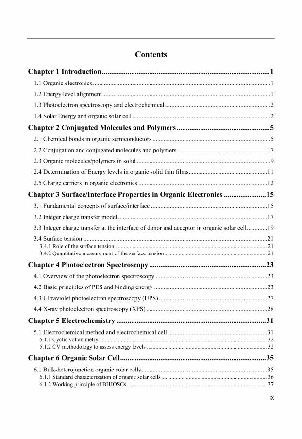
especially in terms of electricity as shown in Figure 1.1.
Figure 1.1 Renewables 2017 Global status report-Estimated renewable energy share of global
electricity production, End 2016[8]
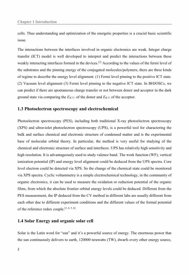
Solar energy can be converted to electric energy by solar cells. At present, the market is dominated
by silicon solar cells due to the high conversion efficiency as shown in Figure 1.2 and high stability.
The huge success and maturity of silicon industry means there is little urgency to develop
alternatives.[7] However, the manufacturing process of the silicon solar cell is complicated and use
a lot of energy.
Organic solar cells with featuring properties of light weight, flexibility and easy solution-based
processing for mass production have the potential of being inexpensive in high volumes for
application. Yet there are two main obstacles that need to be overcome. One is the low power
conversion efficiency as shown in the Figure 1.2 and another one is the stability. The synthesis of
new materials and new device structures are improving the efficiency and stability of the organic
solar cell. The recent reported efficiency of single junction organic solar cell has been pushed to
over 12% and the stability has also been improved,[9] moving the field further forward to
commercialization of OSCs.
Chapter 1 Introduction
4
Figure 1.2 Development of Laboratory Solar Cell Efficiencies (adapted from reference).[10]
Upon the issues mentioned above, this thesis provides a comprehensive study and understanding
on organic electronics, especially organic solar cells, from molecule/polymer level to the integrated
devices and from the efficiency to stability. The thesis illustrates how the energy levels are
determined by different technologies, UPS and CV methods, and explore what is the relationship
between the values measured by different methods. How the energy level alignment affect the
performance of the organic solar cells and how to control the photo voltage in binary and ternary
organic solar cell according to energy level alignment at interface also is explored. The stability
and degradation of n-type non-fullerene materials is studied via in situ method (PES) and we
demonstrate how this kind of materials interact with oxygen and water.
Chapter 2 Conjugated Molecules and Polymers
5
Chapter 2 Conjugated Molecules and Polymers
2.1 Chemical bonds in organic semiconductors
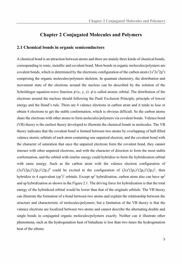
A chemical bond is an attraction between atoms and there are mainly three kinds of chemical bonds,
corresponding to ionic, metallic and covalent bond. Most bonds in organic molecules/polymers are
covalent bonds, which is determined by the electronic configuration of the carbon atom (1s22s22p2)
comprising the organic molecules/polymers skeleton. In quantum chemistry, the distribution and
movement state of the electrons around the nucleus can be described by the solution of the
Schrödinger equation-wave function (x, y, z). is called atomic orbital. The distribution of the
electrons around the nucleus should following the Pauli Exclusion Principle, principle of lowest
energy and the Hund’s rule. There are 4 valence electrons in carbon atom and it tends to lose or
obtain 4 electrons to get the stable conformation, which is obvious difficult. So the carbon atoms
share the electrons with other atoms to form molecules/polymers via covalent bonds. Valence bond
(VB) theory is the earliest theory developed to illustrate the chemical bonds in molecules. The VB
theory indicates that the covalent bond is formed between two atoms by overlapping of half-filled
valence atomic orbitals of each atom containing one unpaired electron, and the covalent bond with
the character of saturation that once the unpaired electrons form the covalent bond, they cannot
interact with other unpaired electrons, and with the character of direction to form the most stable
conformation, and the orbital with similar energy could hybridize to form the hybridization orbital
with same energy. Such as the carbon atom with the valence electron configuration of
(2s)2(2px)1(2py)1(2pz)0 could be excited to the configuration of (2s)1(2px)1(2py)1(2pz)1, then
hybridize to 4 equivalent (sp3)1 orbitals. Except sp3 hybridization, carbon atom also can have sp2
and sp hybridization as shown in the Figure 2.1. The driving force for hybridization is that the total
energy of the hybridized orbital would be lower than that of the originals orbitals. The VB theory
can illustrate the formation of a bond between two atoms and explain the relationship between the
structure and characteristic of molecules/polymers, but a limitation of the VB theory is that the
valence electrons are localized between two atoms and cannot describe the alternating double and
single bonds in conjugated organic molecules/polymers exactly. Neither can it illustrate other
phenomena, such as the hydrogenation heat of butadiene is less than two times the hydrogenation
heat of the ethene.

Chapter 2 Conjugated Molecules and Polymers
6
Figure 2.1 Electron configuration of the carbon atom and hybridization state.
Complementing the VB theory, the molecular orbital (MO) theory was developed later to describe
the covalent bond. MO theory states that electrons are distributed in sets of MOs and can extend
over entire molecule. Like VB theory, the formation of molecular orbitals obeys minimum energy
principle, Hund’s rules and Pauli Exclusion Principle. In quantum mechanics, molecular orbitals
can also be described by the solution of the Schrödinger equation-wave function 1 and the most
popular application of the molecular orbital method is the linear combination of atomic orbitals
(LCAO), including two kinds of molecular orbital, bonding orbital, 1= 1 +2, and anti-bonding
orbital, 2= 1 - 2, showing in Figure 2.2.
Figure 2.2 Linear combination of the atomic orbitals to form bonding orbital and anti-bonding
orbital.

Chapter 2 Conjugated Molecules and Polymers
7
In MO theory, the head on overlapping of the two atomic orbitals form the /* molecular orbital.
The side by side overlapping of the two atomic orbitals could form /* molecular orbital. As
shown in Figure 2.3, for the simple ethylene, the two carbon atoms adopt sp2 hybridization and two
sp2 atomic orbitals form /* molecular orbital by head on overlapping, while the residual p
orbitals overlap side by side to form /* molecular orbital. The formation of the molecular
orbitals make the length of double bond in ethylene shorter than single bond. The formation of the
molecular orbitals can also make the molecule more planar because the free rotation is limited.
Figure 2.3 Formation of the molecular orbital and molecular orbital
2.2 Conjugation and conjugated molecules and polymers
There are mainly three types of conjugation in organic molecules/polymers. They are -, p-
conjugation and - hyper conjugation respectively (Figure 2.4). p- conjugation could be usually
found between the adjacent orbital and p-orbital with paired electrons. The weak - hyper
conjugation exist in the system with the orbital and adjacent C-H bond. The main conjugation
effect in conjugated molecules/polymers with alternating single and double bonds is -
conjugation. One simple example is butadiene as shown in Figure 2.4c, the butadiene could be
considered as the connection of the two ethylene by the elimination of one hydrogen in each
molecule and the unoccupied two sp2 form additional bond between two carbon atoms. Usually,
we only care about the -orbitals in conjugated molecules/polymers. There are should be four -
MO in butadiene and the energy would increase with the increasing of the nodes.

Chapter 2 Conjugated Molecules and Polymers
8
Figure 2.4, p-, -and - conjugation.
There are two occupied -bonding orbitals and unoccupied -anti-bonding orbitals in butadiene
The highest occupied molecular orbital (HOMO) and The lowest unoccupied molecular orbital
(LUMO) are defined as the frontier molecular orbitals.[11] The pair of -electrons occupying the
highest orbital which are referred to as frontier electrons, playing a decisive role both in chemical
activation and optoelectronic properties of the hydrocarbon molecules/polymers. The ionization
potential (IP) is defined as the minimum energy needed when taking one electrons from the HOMO
to the vacuum, and electronic affinity (EA) is defined as the minimum energy released when adding
one electron from the vacuum level to the LUMO. The energy difference between the HOMO and
the LUMO is defined as energy gap. It is well known now that the energy and energy difference
between two orbitals is quantized, so the optical properties are determined by the energy of the MO
and electrons can be excited from occupied orbitals to unoccupied orbitals with absorption of the
energy equal to the energy difference between two orbitals. The energy gap determines the
minimum energy that can be absorbed by the molecules/polymers.
It is easy to imagine that with the increase of the conjugated chain, the bonding and antibonding
orbitals will form a band-like distribution, named valance band and conduction band respectively
as shown in Figure 2.5. With the increase of the conjugated length, the HOMO and the LUMO
would become closer, i.e. The IP would be decreased and the EA would be increased, and the
energy gap between LUMO and HOMO would be decreased.

Chapter 2 Conjugated Molecules and Polymers
9
Figure 2.5 Energy level derivation in -conjugated linear chain.
2.3 Organic molecules/polymers in solid
When the molecule/polymers are stacked into solid materials, the distribution of the bonding and
antibonding orbitals can be further broadened as shown in Figure 2.6 due to interchain - stacking.
Figure 2.6 Energy level derivation in stacked solid state.
For an isolated molecules/polymer, the energy of each MO is discrete. Here we focus on IP and
EA. While the energy of molecular orbitals strongly depends on the local environment, i.e. the
intermolecular order and the nature of surrounding molecules/polymers.[12, 13] In amorphous or
Chapter 2 Conjugated Molecules and Polymers
10
polycrystalline, each molecule has a unique local environment as shown in Figure 2.7, then each
IP and EA will be unique. In this case, although the HOMO and LUMO is unique, and IP and EA
are well defined for each isolated molecule, there will be a broad distribution of the IP and EA for
solid film due to the variations in the local molecular order. The same holds true for polymers.
Besides the situation in molecular solid, the different conjugation length of each polymer makes
the distribution of the IP and EA broader in polymer solid. The broad distribution of the IP in
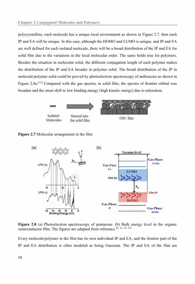
molecule/polymer solid could be proved by photoelectron spectroscopy of anthracene as shown in
Figure 2,8a.[12] Compared with the gas spectra, in solid film, the spectra of frontier orbital was
broaden and the onset shift to low binding energy (high kinetic energy) due to relaxation.
Figure 2.7 Molecular arrangement in the film
Figure 2.8 (a) Photoelectron spectroscopy of pentacene. (b) Bulk energy level in the organic semiconductor film. The figures are adapted from reference.[9, 12, 14, 15]
Every molecule/polymer in the film has its own individual IP and EA, and the frontier part of the
IP and EA distribution is often modeled as being Gaussian. The IP and EA of the film are

Chapter 2 Conjugated Molecules and Polymers
11
represented by the smallest individual IP and largest individual EA. The actual energy gap in
organic solid film is then defined by the upper edge of the IP energy distribution and the lower
edge of the EA energy distribution. The energy level diagram could be summarized in Figure 2.8b.
According to the definition of the actual energy gap, for the non-degenerate materials, there are
consequently no gap states in absence of doping or molecular defects as the frontier IP/EA energies
created by variations.
2.4 Determination of Energy levels in organic solid thin films
The definition of each item has been clarified and defined as described above. In the field of organic
electronics, one of the most important tasks during design and fabrication of organic devices is to
measure the energy levels of the organic materials appropriately and understand the energy level
alignment at the interfaces involving semiconducting molecules and polymers.[16, 17] For instance,
the electron affinity (EA) of an electron-transporting organic material should be larger than a
threshold value (~3.6 eV) so as to get electron-trap-free transport and stable devices,[18, 19, 20] while
the energy level alignment at interfaces will affect charge injection, free charge generation, charge
transport and extraction.[2, 9, 14, 16] The determination of energy levels, mainly IP and EA, hence is
crucially important and constitutes an important step towards making efficient and stable
devices.[21] Commonly used methods to determine energy levels in thin film materials and energy
level alignment at interfaces include ultraviolet photoelectron spectroscopy (UPS),[2] inverse
photoemission spectroscopy (IPES),[22, 23] cyclic voltammetry (CV) and quantum chemical
calculation,[22, 24] sometimes assisted by Kelvin probe (interface potential steps)[25] and UV-vis
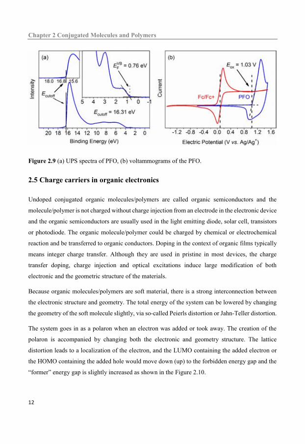
(band gap) measurements.[22, 26] In this thesis, the value of IP and EA are deduced from the UPS
spectra assistant by UV-vis absorption or voltammograms. Two kinds of spectra are shown in
Figure 2.9. These two kinds of related technologies and methods will be described in detail in
Chapter 4 and chapter 5 respectively.
Chapter 2 Conjugated Molecules and Polymers
12
Figure 2.9 (a) UPS spectra of PFO, (b) voltammograms of the PFO.
2.5 Charge carriers in organic electronics
Undoped conjugated organic molecules/polymers are called organic semiconductors and the
molecule/polymer is not charged without charge injection from an electrode in the electronic device
and the organic semiconductors are usually used in the light emitting diode, solar cell, transistors
or photodiode. The organic molecule/polymer could be charged by chemical or electrochemical
reaction and be transferred to organic conductors. Doping in the context of organic films typically
means integer charge transfer. Although they are used in pristine in most devices, the charge
transfer doping, charge injection and optical excitations induce large modification of both
electronic and the geometric structure of the materials.
Because organic molecules/polymers are soft material, there is a strong interconnection between
the electronic structure and geometry. The total energy of the system can be lowered by changing
the geometry of the soft molecule slightly, via so-called Peierls distortion or Jahn-Teller distortion.
The system goes in as a polaron when an electron was added or took away. The creation of the
polaron is accompanied by changing both the electronic and geometry structure. The lattice
distortion leads to a localization of the electron, and the LUMO containing the added electron or
the HOMO containing the added hole would move down (up) to the forbidden energy gap and the
“former” energy gap is slightly increased as shown in the Figure 2.10.

Chapter 2 Conjugated Molecules and Polymers
13
Figure 2.10 Energy level of neutral conjugated molecular/polymer polaron and bi-polaron.

Chapter 2 Conjugated Molecules and Polymers
14

Chapter 3 Surface/Interface Properties in Organic Electronics
15
Chapter 3 Surface/Interface Properties in Organic Electronics
3.1 Fundamental concepts of surface/interface
An interface represents the boundary between two phases, including solid-liquid interfaces, solid-
gas interfaces, solid-solid interfaces, solid-vacuum interfaces, liquid-liquid interfaces and liquid –
gas interfaces. Solid-gas interface and liquid gas interface are also called surface due to the
attendance of the gas.
In organic electronics, the devices are made of different layers with different functions via
deposition of e.g. one material on the surface of the other, as shown in Figure 3.1 for the organic
solar cell with conventional structure, so the interfaces between the solid would be formed when
the -conjugated molecules/polymers are brought into contact with the surface of another material.
The interface involved in organic electronic devices mainly includes organic/metal and
organic/organic interface, and the key electronic processes such as charge injection, extraction,
charge dissociation and recombination occur at these interfaces, and all these processes play an
important role in the device performance. Thus, it is important to figure out the interface properties
of both organic/metal and organic/organic interface.
Figure 3.1 Conventional structure of organic solar cell
When a -conjugated molecule/polymer is brought into contact with the surface of another material,
the absorption process may result in a wide variety of effects at the interface and the energetic

Chapter 3 Surface/Interface Properties in Organic Electronics
16
properties of organic molecules/polymers at interfaces typically will be different from the bulk.
These interface effects including: polarization of the electron density of the organic material due
to interaction with an image charge on the substrate surface, partial charge transfer through
covalent organic–substrate bonds, integer charge transfer through tunneling across the
organic/substrate interface, surface rearrangement by (inter) diffusion across the organic/substrate
interface, adsorption-induced order or disorder. According to the interaction strength, the types of
interface can be categorized to five kinds as shown in Table 3.1.
Table 3.1 Interfaces involved in organic electronics. The Table is adapted from reference.[2]
Example of interface Interaction type
Noble gas atoms or saturated hybrocabons on clean metal surfaces[27, 28, 29, 30]
(1) Physisorption, absence of charge transfer
-conjugated molecules and polymers on organic or passivated metal surfaces[31, 32]
(2) Physisorption, possible integer electron
charge transfer through tunneling
-conjugated molecules on non-reactive clean metal surfaces[33, 34]
(3) Weak chemisorption, possible partial charge
transfer
(-conjugated) molecules on reactive clean metal surfaces[35]
(4) Strong chemisorption, covalent bonding
between molecule and metal, (partial charge
transfer)
(-conjugated) molecules with intrinsic dipole and anchoring groups on clean metal surfaces[36, 37]
(5) Strong chemisorption, covalent bonding at
specific sites of molecule and metal, (partial)
charge transfer, intrinsic dipole
Although there is no unified model to describe all these kind of interfaces mentioned above, models
exist that successfully describe subsets of different interface types. The electronic properties of the
interface that are characterized by negligible hybridization of -electronic molecular orbitals and
substrate wave functions could be explained and predicted by ICT model.[32, 38] In Organic
electronics, due to the processing conditions such as solution processing of molecules/polymers
via spin coating or printing, the organic semiconductor films typically are physisorbed on the
substrates to form such interfaces. More generally, semiconducting organic/organic interfaces and
Chapter 3 Surface/Interface Properties in Organic Electronics
17
interfaces formed with substrates that are passivated by oxides or residual hydrocarbons also fall
in this category. The residual of hydrocarbons or oxide would prevent hybridization of electronic
states and thus blocking the formation of interface dipoles via partial electron charge transfer. But
electron transfer can still occur by tunneling as long as the passivating layer is thin enough. The
tunneling of the electrons through the interface passivating layer implies integer charge transfer.
3.2 Integer charge transfer model
The ICT model predicts and explains the experimentally verified abrupt transitions between a
vacuum level alignment regime and Fermi-level pinning regimes upon variations of the work
function of the substrate. The Fermi-level pinning regimes feature a potential step that scales with
the difference between the equilibrium ionization potential or electron affinity of the organic
semiconductor at the interface and the work function (SUB) of the substrate. The origin of the
potential step is explained by spontaneous charge transfer across the interface via tunneling (integer
charge transfer) when the substrate work function is higher than the energy required to take away
one electron (lower than the energy gained from adding one electron) from (to) the molecule at an
interface producing a fully relaxed state. The most easily oxidized donor molecules (or segments
on polymers) hence will be “used up” until enough charge has been transferred across the interface
to create a potential step that equilibrates the Fermi level. The energy where the Fermi level is
subsequently pinned is referred to as pining energy (EICT+,-). The energy of a positive integer charge
transfer state, ICT+, is defined as the energy required to take away one electron from the
molecule/polymer producing a fully relaxed state, that is, both electronic and geometrical
relaxation are included as well as screening from the substrate. The energy of a negative integer
charge-transfer state, ICT-, is defined as the energy gained when one electron is added to the
molecule/polymer producing a fully relaxed state, that is, both electronic and geometrical
relaxation are included as well as screening from the substrate. Thus, the pinning energy is similar
in nature but differ from the ionization potential (IP) and electron affinity (EA) of the organic
semiconductor, i.e. the polaronic transport states, such as EICT+ = IP – B+ and EICT- = EA + B-,
where B+ (B-) is the Coulomb energy associated with charging a molecule in the interface layer
with an hole (electron),[38, 39] and are thus moved into the gap compared to the bulk polarons (IP/EA)

Chapter 3 Surface/Interface Properties in Organic Electronics
18
Three distinct energy level alignment regimes are predicted by the ICT model and the detail are
described as following and process are shown in Figure 3.2.
(i) SUB EICT- Fermi level pinning to a negative integer Charge transfer state; substrate
independent resulting work function ORG/SUB
(ii) EICT- SUB EICT+ Vacuum level alignment; substrate dependent resulting work function
ORG/SUB; slope = 1
(iii) SUB EICT+ Fermi level pinning to a positive integer charge transfer state; substrate-
independent resulting work function ORG/SUB
Figure 3.2 Typical energy level alignment behavior for weakly interacting organic semiconductor interfaces that follow the ICT model, where the resulting work function (ORG/SUB) is either independent (i, iii) or linearly dependent with a slope of ~1 (ii) of the substrate work function (SUB) and Schematic illustration of the evolution of the energy-level alignment when a conjugated organic molecule or polymer is physisorbed on a substrate surface. The figure is adapted from reference.[2]
As we described in chapter 2, the frontier parts of the resulting occupied and unoccupied state
distributions forming the energy gap are often modeled as being Gaussian. Now, taking
Chapter 3 Surface/Interface Properties in Organic Electronics
19
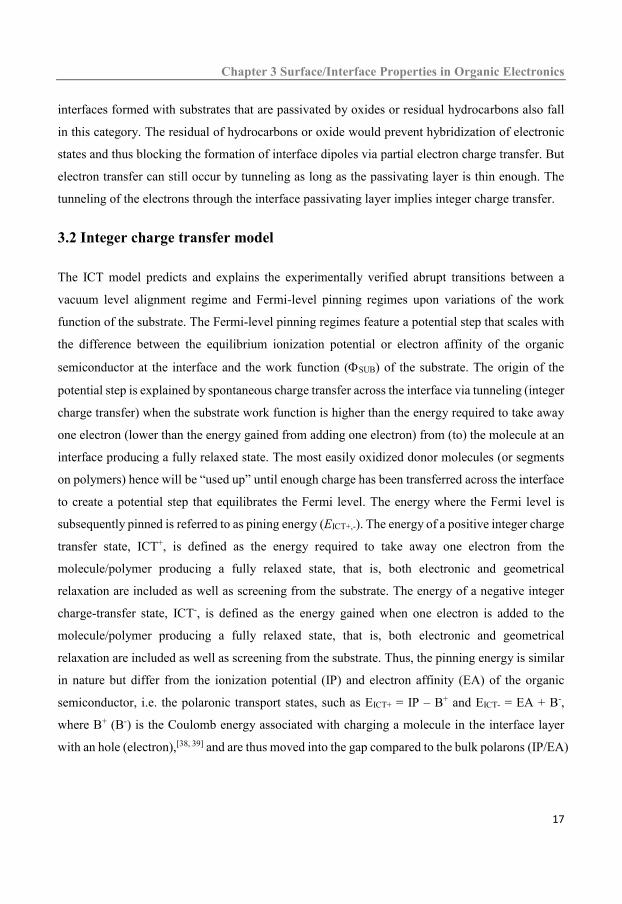
EICT+/EICT+,- and IP/EA together, the evolution of the energetic from interface to bulk can be
summarized in Figure 3.3.
Figure 3.3 Diagram showing energy level alignment including the ICT state and bulk frontier density of state distribution. Here the Fermi level becomes pinned to the EICT+ (oxidation of molecules at the interface causing Fermi level equilibrium). The figure is adapted from reference.[9,
14, 15]
3.3 Integer charge transfer at the interface of donor and acceptor in organic
solar cell
In organic electronic devices, besides the organic/metallic interfaces, there are organic/organic
heterojunction interfaces, which are characterized by weak van der Waals intermolecular bonding
and can be considered as nearly non-interactive. So the ICT model can not only explain and predict
the energy level alignment at organic/metal interfaces, but also can be successfully applied to
various cases of heterojunctions comprised of organic semiconductors, where the relative position
between the -conjugated organic molecules/polymers integer charge transfer states determines the
energetic alignment at the organic/organic interfaces.[2, 40, 41, 42]
The active layer of organic solar cells is composed of donor(s) and acceptor(s), implying there are
organic/organic interfaces as shown in Figure 3.1. The energy level alignment diagram between an
adjacent donor and acceptor are shown in the Figure 3.4. When the EICT+ of the donor is larger than
the EICT- of the acceptor, the vacuum level would be alignment, meaning that there is not charge
transfer between donor and acceptor under the dark ground state (Figure 3.4a). In contrast, when
the EICT+ of the donor is smaller than the EICT- of the acceptor, there would be spontaneous charge
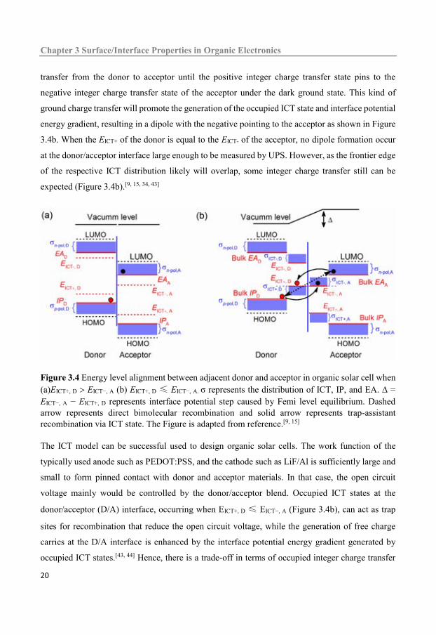
Chapter 3 Surface/Interface Properties in Organic Electronics
20
transfer from the donor to acceptor until the positive integer charge transfer state pins to the
negative integer charge transfer state of the acceptor under the dark ground state. This kind of
ground charge transfer will promote the generation of the occupied ICT state and interface potential
energy gradient, resulting in a dipole with the negative pointing to the acceptor as shown in Figure
3.4b. When the EICT+ of the donor is equal to the EICT- of the acceptor, no dipole formation occur
at the donor/acceptor interface large enough to be measured by UPS. However, as the frontier edge
of the respective ICT distribution likely will overlap, some integer charge transfer still can be
expected (Figure 3.4b).[9, 15, 34, 43]
Figure 3.4 Energy level alignment between adjacent donor and acceptor in organic solar cell when (a)EICT+, D EICT−, A (b) EICT+, D ≤ EICT−, A. σ represents the distribution of ICT, IP, and EA. ∆ = EICT−, A − EICT+, D represents interface potential step caused by Femi level equilibrium. Dashed arrow represents direct bimolecular recombination and solid arrow represents trap-assistant recombination via ICT state. The Figure is adapted from reference.[9, 15]
The ICT model can be successful used to design organic solar cells. The work function of the
typically used anode such as PEDOT:PSS, and the cathode such as LiF/Al is sufficiently large and
small to form pinned contact with donor and acceptor materials. In that case, the open circuit
voltage mainly would be controlled by the donor/acceptor blend. Occupied ICT states at the
donor/acceptor (D/A) interface, occurring when EICT+, D ≤ EICT−, A (Figure 3.4b), can act as trap
sites for recombination that reduce the open circuit voltage, while the generation of free charge
carries at the D/A interface is enhanced by the interface potential energy gradient generated by
occupied ICT states.[43, 44] Hence, there is a trade-off in terms of occupied integer charge transfer

Chapter 3 Surface/Interface Properties in Organic Electronics
21
state density and the sweet spot occurs at EICT−, A ≈ EICT+, D.[9, 15, 43] More details will be discussed
in chapter 7.
3.4 Surface tension
3.4.1 Role of the surface tension
Organic molecules/polymers are solution processable, which allows for manufacturing of organic
electronic devices on various substrates by common technics such as spin-coting and printing. Thus,
the structure of the film forms dynamically during it’s solidification from a solution and the final
structure of the film depends strongly on processing condintions and materials properties of the
components, one of which is the surface tension. Both of the surface tension of the substrate and
the organic molecules/polymers plays an important role in the process of electrochemical and
electronic devices preparation.
The surface tension of the substrate will affect the buried interface component during the deposition
of the blend film, and it can be tuned or even actively controlled via replacement or modification
of the substrate.[45, 46, 47] The surface tension of the organic molecules/polymers can affect the phase
seggragation and determin the vertical phase separation of the blend film.[13, 48, 49] The materials
with lower surface energy is likely to be segregated into the air/film interface, while the materials
with higher surface energy tend to segregate to the film/substrate interface. In organic solar cells,
it would be beneficial to charge collection having the hole tranporting phase of the active layer
adjacent to the anode and the electron transporting phase adjacent to the cathode.
Not only can the surface energy be the driving force of the vertical distribution but also it can be
the driving force of the location for a third component in ternary blends.[9, 15, 50, 51] The later case
will be discussed in Chapter 8.
3.4.2 Quantitative measurement of the surface tension
The surface energy of a material M can be estimated from the contact angle of ultrapure water on
spin coated films of material M. As shown in Figure 3.5, the angle between the liquid-gas
interface and solid-liquid interface is defined as contact angle. The surface (interficial) tension
(surfce energy) is represented by . S-L represents interfacial energy between solid and liquid, L-G
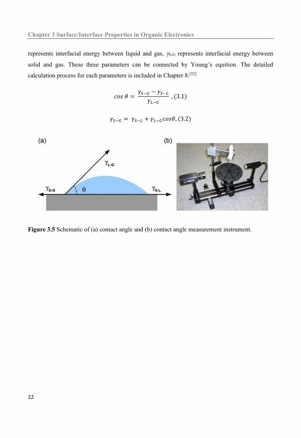
Chapter 3 Surface/Interface Properties in Organic Electronics
22
represents interfacial energy between liquid and gas, S-G represents interfacial energy between
solid and gas. These three parameters can be connected by Young’s equition. The detailed
calculation process for each parameters is included in Chapter 8.[52]
𝑐𝑜𝑠 𝜃 = 𝛾𝑆−𝐺 − 𝛾𝑆−𝐿
𝛾𝐿−𝐺 , (3.1)
𝛾𝑆−𝐺 = 𝛾𝑆−𝐿 + 𝛾𝐿−𝐺𝑐𝑜𝑠𝜃, (3.2)
Figure 3.5 Schematic of (a) contact angle and (b) contact angle measurement instrument.
Chapter 4 Photoelectron Spectroscopy
23
Chapter 4 Photoelectron Spectroscopy
4.1 Overview of the photoelectron spectroscopy
PhotoElectron Spectroscopy (PES), also called PhotoEmission Spectroscopy (PES), is based on
the photoelectric effect discovered by Hertz in 1887 and explained by Einstein in 1905 via invoking
the quantum nature of the light. Different from other conventional methods of spectroscopy in that
PES detects electrons rather than photons to study electronic structure of materials. Nowadays, it
has been developed into powerful and widely used techniques in academic basic research as well
as in industry. Not only does PES provide the experimental basis for molecular orbital theories but
it is also an important tool for surface analysis. The information provided by photoelectron
spectroscopy includes the following.
Surface chemical states, including the type and the content of the elements, chemical
valance states, the formation of the chemical bonds.
Surface structure, including morphology, phase aggregation, elements distribution and
atomic arrangement.
Surface electronic state, including distribution of the surface electrons, energy level and
energy level alignment at surface.
The widely application of the PES could be attributed to many advantages of this measurement,
including that
There is a maximum amount of both chemical and electronic information (listed above)
within a single measurement.
It is typically non-destructive to organic systems.
It is surface sensitive.
4.2 Basic principles of PES and binding energy
PES can measure the energy, intensity and spacial distribution of the photoelectrons emitted from
the materials. Starting from the isolated molecule, the physical process of photo ionization process
can be expressed by the Formula 4.1

Chapter 4 Photoelectron Spectroscopy
24
𝑀 + ℎ𝜈 → 𝑀+∗ + 𝑒−, (4.1)
The molecule M is excited to M+* by a photon with the energy hv and an electron (e-) is emitted
with the kinetic energy Ek. As we know, the energy of the molecule is the eigenvalue of the
Schrödinger equation
Ĥ𝑖 = 𝐸𝑖𝑖, (4.2)
According to energy conversation
𝐸𝑖(𝑛) + ℎ𝜈 = 𝐸𝑓(𝑛 − 1) + 𝐸𝑘, (4.3)
or
𝐸𝐾 = ℎ𝜈 − (𝐸𝑓(𝑛 − 1) − 𝐸𝑖(𝑛)), (4.4)
Where Ei (n) is the energy of the ground state of molecules with n electrons and Ef (n-1) is the
energy of final state of ionized molecules with (n-1) electrons. The binding energy (EB) is defined
as
𝐸𝐵𝑉 = 𝐸𝑓(𝑛 − 1) − 𝐸𝑖(𝑛)) = ℎ𝜈−𝐸𝐾 , (4.5)
Thus EB represents the energy difference between the initial ground state and various final exited
states and could be calculated by delta-self-consistent field (SCF) according to Koopmans rule
that the wave function of other electrons do not change when an electron is taken away from the
molecule. i.e. the binding energy is equal to the negative energy of the orbital from which the
photoelectron is emitted. But the reality is that both of intramolecular electron relaxation and
nuclear geometric relaxation will happen following the emitting of the electron to screen the core
hole and to minimize the total energy of the final ionized state. The relaxation would lead to a
decrease of expected binding energy defined in Formula (4.5). It should be noted that in PES
measurement, the photoelectrons leave the molecule typically within about 10-15 s during the photo
emitted process, while the electronic relaxation time is around 10-16 s, and the nuclear geometric
relaxation time is around 10-13 s.[53] Thus, the electrons have had time to relax, that is, the hole is
fully screened, but the nuclei are frozen during the process. This means that PES measurement will
Chapter 4 Photoelectron Spectroscopy
25
overestimate the binding energy and the final hole-polaron formation energy in general due to that
the energy of ionized final-state would be further decreased by geometric relaxation.
In the solid, the binding energy are conventionally measured with respect to the Fermi level instead
of the vaccum level, and the binding energy could be expressed by
𝐸𝐵𝐹 = ℎ𝜈−𝐸𝐾 − , (4.6)
Where represent the work function of the solids. In organic molecule/polymer solids, the
intermolecular relaxation of the surrounding molecules provides addition screening of the hole,
which will increase the kinetic energy and decrease the binding energy further compared to isolated
molecule. The rigid shift caused by the intermolecular polarization effects could be observed in
Figure 2.8a.
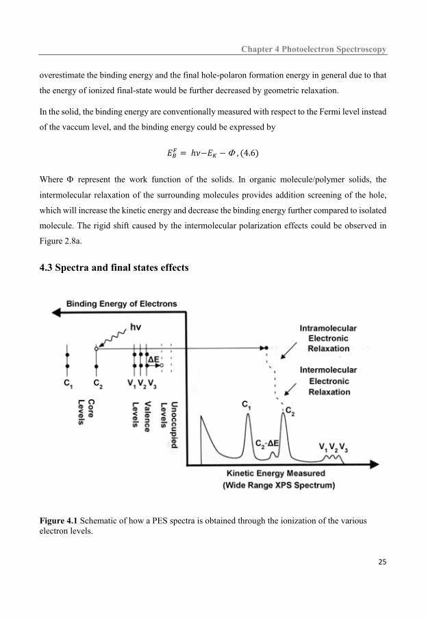
4.3 Spectra and final states effects
Figure 4.1 Schematic of how a PES spectra is obtained through the ionization of the various electron levels.

Chapter 4 Photoelectron Spectroscopy
26
For a given photo energy, recoding the number of photoelectrons as a function of their kinetic
energy yields a spectra of distinct line as shown in the Figure 4.1, reflecting the energy distribution
of the occupied orbital. In general, the spectra are recorded with EB as the abscissa according to
equation (4.6). Depending on the energy of the photon source, the PES is divided into Ultraviolet
photoelectron spectroscopy (UPS) and X-ray photoelectron spectroscopy (XPS). UPS can measure
the electrons coming from the valence orbital and XPS can measure the electrons in the core levels
as well.
PES always measure the final state energies that can be related to the initial state. As discussed
above, the main photoelectron line would shift to lower binding energy rather than at the binding
energy of the neutral state due to electron relaxation as shown in Figure 4.1. Thus the relaxation of
the electron system in response to the creation of a hole is one of important final state effects.
Another kind of the final state effects is multi-electron excitations. During the emission process of
the electrons, a variety of electronically excited final states would be created in company with the
core level ionization state and the satellite lines would be recorded in the spectra. According to
energy conservation, the excitation energy would be missing from the kinetic energy, leading to
the satellite lines shift to high binding energy ((C2-E1) in Figure 4.1)) compared to the main line.
Some most important final states are shown in Figure 4.2
Figure 4.2 Schematic of various final states. The figure is adapted from reference.[54]

Chapter 4 Photoelectron Spectroscopy
27
4.3 Ultraviolet photoelectron spectroscopy (UPS)
UPS refers to the measurement of kinetic energy spectra of photoelectrons emitted from the
materials which is excited by a low energy ultraviolet light source. UPS technique is analogous to
XPS but with orders of magnitude higher photoionization cross-section and higher resolution. The
source of photons usually used are HeI (hν 21.2 eV) radiation and HeII radiation (hν 40.8 eV).
The valence electronic states of materials can be mapped out in the form of the spectrum with the
intensity as the function of the binding energy. The full UPS spectra of both a gold substrate and a
polymer over-layer on the gold substrate are shown in the Figure 4.3. The occupied electronic
structure, the work function () and the change in the work function () that can occur upon
coverage of the substrate surface can be derived from the UPS spectra.
Figure 4.3 The full UPS spectra of both a gold substrate (left) and a polymer over-layer on the gold substrate (right). The figure is adapted from reference.[2]
The vacuum level of a metal substrate as measured by UPS corresponds to the energy of an electron
at rest just outside the sample instead of the electron at the infinite distance and it is still affected
by the potential of the solid.[17] Work function is an important parameter that determines the
minimum energy necessary to remove an electron from the material. The work function could be
obtained from the measured energy of the secondary-electron cutoff (Ecutoff) according to formula

Chapter 4 Photoelectron Spectroscopy
28
(4.6) and (4.7), and the change in work function () could be derived by measuring the Ecutoff of
the substrate with the overlayer as shown in Figure 4.3.
= ℎ𝜈 − 𝐸cutoff, (4.7)
The offset between the valence band edge of the overlayer and the fermi energy in conducting
substrate, represented by EF VB, determines the hole injection barriers. According to formula 4.6, the
electrons with maximum kinetic energy must be emitted from the fermi level of the metal substrate
or valence band edge of the polymer, represented by EMax K (metal) and EMax
K (polymer) respectively.
In this case, the offset represents the kinetic energy difference between the fastest photoelectrons
from fermi level of the metal substrate and from the valence band edge of the polymer over-layer.
The energy difference between the vacuum level of the polymer over-layer and the fermi energy
in the conducting substrate (EVac F ) is given by formula (4.8)
𝐸𝐹𝑉𝑎𝑐 = ℎ𝑣 − (𝐸𝐾
𝑀𝑎𝑥(𝑝𝑜𝑙𝑦𝑚𝑒𝑟) + 𝐸𝑉𝐵𝐹 ), (4.8)
The offset between the vacuum levels of the polymer-covered substrate and the clean gold substrate
arises from the existence of dipole at the interface and can be expressed by formula (4.9).
∆ = 𝐸𝐹𝑉𝑎𝑐 − 𝐴𝑢, (4.9)
The ionization potential (IP) for the molecule/polymer is a material constant and should not depend
upon the substrate.
𝐼𝑃 = 𝐸𝑉𝐵𝐹 + 𝐸𝐹
𝑉𝑎𝑐 , (4.10)
EA is also materials constant, but it cannot be measured via UPS due to there are no electrons to
photoemit, so inverse photoemission spectroscopy (IPES) instead can be used to obtain EA. The
EA could also be obtained by adding the optical band gap to the IP measured by UPS. Another
simple method to measure IP and EA is the electrochemical method that will be described in
Chapter 5.
4.4 X-ray photoelectron spectroscopy (XPS)
The commonly used light sources in XPS are Mg(Ka) with the photo energy of 1253.7 eV or Al(Ka)
radiation with the photo energy of 1486.6 eV. In XPS measurements, the core electronic properties
Chapter 4 Photoelectron Spectroscopy
29
of materials can be mapped due to the high light radiation energy. It’s easy to understand that the
binding energy of core electrons for each element would be different and the exact value of the
binding energy of a distinct atom also depends on the chemical environment. An energy shift will
occur when chemically inequivalent atoms of the same elemental species are present and these
energy shifts are named chemical shifts. By comparison with the data of standard substances, the
chemical shift can be used to determine the oxidation state and chemical bonds. Thus the XPS can
be used to detect the distribution of each component at surface according to the ratio of each
elements or the feature elements in different component. One example is that the XPS can be used
to identify the vertical distribution of the blend film. The vertical distribution of the donor and
acceptor is important for charge extraction in organic solar cell as mentioned in Chapter 3. The
change of the chemical environment can be recorded by XPS, so it can be used to track the process
of doping, oxidation or adsorption. In this thesis, XPS are used to exam the degradation of the n-
type organic electronics in air atmosphere.

Chapter 4 Photoelectron Spectroscopy
30
Chapter 5 Electrochemistry
31
Chapter 5 Electrochemistry
5.1 Electrochemical method and electrochemical cell
Electrochemistry is a branch of physical chemistry and it studies the relationship between chemical
changes and electrical effect. The chemical energy and electrical energy can be converted and this
conversion is accomplished by ionic current flow in an electrolyte solution between two electrodes
connected to each other via an external circuit with an electrical load or current source. Devices
such as batteries and fuel cells can convert the energy from chemical reactions into electrical energy,
while electrolysis and some electro-analysis can reverse this conversion direction.
Although there are many different kinds of instrumentation, all these electrochemical
measurements are conducted in an electrochemical cell which is the basic component of various
electrochemical instrument and consists of two or more electrodes and the electronic circuitry for
controlling and measuring the current and the potential. Two electrode electrochemical cell consists
of a working electrode and a counter electrode immersed in electrolyte solution, while there is an
additional reference electrode in three electrode system as shown in Figure5.1.
Figure5.1 Schematic of the three electrode cell configuration

Chapter 5 Electrochemistry
32
5.1.1 Cyclic voltammetry
Cyclic voltammetry (CV) is a simple and common used electrochemical technique. In the CV
experiment process, the voltage applied to the working electrode is scanned linearly from initial
value to a predetermined limit where the direction of the scan is reversed. The scan process can be
halted at any point when necessary. The current is plotted as a function of potential to yield a
voltammogram. Three electrode systems are used in CV experiments to make sure that the current
passing between the working and counter electrode and the potential of working electrode (WE)
relative the reference electrode (RE) can be measured. The classical electric circle of three electrode
system is shown in the Figure 5.2. The electrolytic cell consists of a working electrode onto which
the reaction takes place, a reference electrode that maintains the constant potential, and the counter
electrode that supplies the reaction current. The potentiostat supplies a desired cell potential
between WE and RE, and measures the reaction current between WE and CE.
Figure5.2 Classical three electrode circuit used in CV measurement.
5.1.2 CV methodology to assess energy levels
Determination of the energy levels of the conjugated molecules/polymers is the prerequisite to
design efficient and stable organic electronic devices, especially in organic light emitting diodes or
organic solar cells. Besides photoelectron spectroscopy, CV is another important methodology
commonly used in organic electronics to measure the energy levels of the conjugated
molecules/polymers, although there is little consensus in the community on how to use this
technique and how the measurements relate to the vacuum scale.[6, 55] CV methods employed to

Chapter 5 Electrochemistry
33
measure the reduction and oxidation potentials of conjugated molecules/polymers involve the
deposition of the organic conjugated materials onto the working electrode. The oxidation process
of the conjugated molecules/polymers cannot be equal to the reverse reduction process. So the
oxidation and reduction potentials are usually estimated by the onset potential,[56] defined as the
potential at which the initial injection of holes or electrons to the HOMO and LUMO, respectively.
According to the IUPAC recommendations,[57] The oxidation or reduction potential are usually
measured against the potential of the Fc+/Fc redox couples because this potential show little
variations. The energy of HOMO and LUMO (or IP and EA) could be deduced from equation (5.1)
and (5.2) respectively (Figure 5.3).
𝐸𝐻𝑂𝑀𝑂 = −(𝐸𝑜𝑛𝑠𝑒𝑡,𝑂𝑋 𝑣𝑠.𝐹𝑐+ 𝐹𝑐⁄ + 𝐸0′)(5.1)
𝐸𝐿𝑈𝑀𝑂 = −(𝐸𝑜𝑛𝑠𝑒𝑡,𝑟𝑒𝑑 𝑣𝑠.𝐹𝑐+ 𝐹𝑐⁄ + 𝐸0′)(5.2)
Where E0 is the formal potential of the Fc+/Fc. When the formal potential of the NHE is -4.456 eV,
its value is approximately -5.1 eV in fermi scale assuming its value of 0.4 e V versus SCE in
acetonitrile and the potential of SCE versus NHE is 0.2414 eV. The formal potential of the Fc+/Fc
in fermi scale usually used in the community could also be 5.39eV or 4.8eV. Different values of
formal potential in the equation is used in different labs. Therefore, the frontier orbital energy levels
obtained with different scales should not be compared directly.
Figure 5.3 Energy level diagram in cyclic voltammetry measurement.

Chapter 5 Electrochemistry
34
Chapter 6 Organic Solar Cell
35
Chapter 6 Organic Solar Cell
6.1 Bulk-heterojunction organic solar cells
Organic solar cells (OSCs) are attracting research’s attention due to the advantages of cheap, light
weight and flexible etc., and a lot of efforts have been devoted to understanding the working
mechanism and improving the performance of the bulk heterojunction organic solar cells
(BHJOSCs) during last two decades. In BHJOSCs,[58] the active layer is composed of mixture of
donor(s) and acceptor(s) that could form interpenetrating network of donor and acceptor with
massive D/A interfaces. The penetrating network can support charge transport through the active
layer and the D/A interfaces can help exciton dissociation, both of which contribute significantly
to improve the performance of the OSCs. The introduction of the BHJOSCs solves the problem of
large binding energy of the excitons in the first generation single layer OSCs[59] and the problem
of inefficient exciton dissociation in the second generation bilayer OSCs.[60] According to the
components of the active layer, the BHJOSCs can be divided into binary OSCs and multiple-
junction OSCs. In binary organic solar cell, the active layer is just composed of one pair of donor
and acceptor. In multiple-junction OSCs, the component of the active layer is more than one donor
or/and one acceptor. In BHJOSCs, the active layer is sandwiched between two electrodes, and
according to the function of the electrodes, the structure of the devices can be divided into
conventional structure (Figure 6.a) and inverted structure (Figure 6.1b). In conventional structure,
the bottom transparent electrode is the anode, while in inverted structure, the bottom transparent
electrode is the cathode.
Figure 6.1 Conventional and inverted structure of BHJOSCs.

Chapter 6 Organic Solar Cell
36
6.1.1 Standard characterization of organic solar cells
The energy supply for organic solar cell is the photons coming from the sun and the actual spectrum
impinging on the cell in operation can vary due to weather, season, time of day, and location. So
standard illumination air Mass (AM) 1.5G with an intensity of 100 (mW/cm2) is used.[61] The
standard spectra allows the evaluation and comparisons of solar cells performance in different
laboratory. Under standard illumination, the power generates from the solar cell is a product of
photocurrent and photo voltage acting on the external load. So the extraction of power depends on
both the solar cell itself and the external load. The maximum power output can be obtained when
the external load is optimized. The applied voltage sweep simulates different resistor and the
optimum external load can be determined via recording the J-V curve (Figure 6.2).
Figure6.2 Typical Current-Voltage (J-V) curve and power-voltage (P-V) curve of an organic solar cell under AM-1.5G illumination. (PTB7-Th: PBDTTS-FTAZ: PC71BM). The figure is adapted from reference.[15]
The quantity Pout has its best value at the maximum power point (Pmax) as shown in the Figure6.2.
When the photon impingement area is equal to the current generating area, the best thermodynamic
efficiency of the photovoltaic energy conversion process for the solar cell can be expressed by
equation 6.1.

Chapter 6 Organic Solar Cell
37
𝑃𝐶𝐸 = 𝑃𝑚𝑎𝑥
𝑃𝑖𝑛=
𝐽𝑚𝑝 ∗ 𝑉𝑚𝑝
𝑃𝑖𝑛, (6.1)
The ideally shaped J-V characteristic would be rectangular and would deliver a constant current
density Jsc until the open circuit voltage Voc. In this case the maximum power point would have a
current density of Jsc and voltage of Voc. The fill factor (FF) has been invented to measure how
close a given characteristic is to conforming to the idea rectangular J-V shape.
𝐹𝐹 =𝐽𝑚𝑝 ∗ 𝑉𝑚𝑝
𝐽𝑠𝑐 ∗ 𝑉𝑜𝑐, (6.2)
According to the definition of the FF, it should also be the ratio between the area of rectangle A
and the area of rectangle B in the Figure 6.2
After introducing FF, combining equation 6.1 and equation 6.2, the power conversion efficiency
can be rewritten as
𝑃𝐶𝐸 = 𝐹𝐹 ∗ 𝐽𝑠𝑐 ∗ 𝑉𝑜𝑐
𝑃𝑖𝑛, (6.3)
6.1.2 Working principle of BHJOSCs
The working process of BHJOSCs from photon absorption to charge extraction can be described
by the following six steps that are also shown in Figure 6.3, and efficiency of each step are
represented by .
a. a light absorption process which causes a transition in a material (the absorber) from a
ground state to an excited state, (Exciton Generat. or A)
b. Diffusion of excitons to D/A interfaces. (Exciton Diff. )
c. Exciton dissociation and charge transfer (CT) exciton formation at D/A interfaces (Exciton Diss. )
d. CT exciton dissociation and charge separation at the D/A interfaces (CT Diss.)
e. Free charge transport (Charge Trans. )
f. Charge carrier collection at the electrodes and combing with an arriving positive-charge
carrier and returning the absorber to the ground state. ( charge coll. )

Chapter 6 Organic Solar Cell
38
Figure 6.3 Schematic working principle of BHJOSCs.
6.2 Efficiency of Organic Solar Cell
There are three approaches to express the efficiency of the organic solar cell. They are power
conversion efficiency, external quantum efficiency and internal quantum efficiency respectively.
6.2.1 Power conversion efficiency
As discussed at the beginning of this chapter, the power conversion efficiency is defined as the
ratio between maximum output power and incident power of the sun, and can be expressed as
formula 6.4 after introduction of the fill factor.
𝑃𝐶𝐸 = 𝐹𝐹 ∗ 𝐽𝑠𝑐 ∗ 𝑉𝑜𝑐
𝑃𝑖𝑛, (6.4)
6.2.2 External Quantum Efficiency
The externally measured ratio of the number of collected charges (Nout charge) to the number of incident
photons (NIn photon) of a particular wavelength is referred to as the external quantum efficiency (EQE)
of photovoltaic devices, also referred to as incident photon to converted electron efficiency (IPCE)
and can be expressed by formula 6.5.
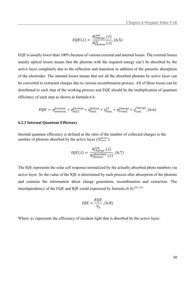
Chapter 6 Organic Solar Cell
39
𝐸𝑄𝐸() = 𝑁𝑐ℎ𝑎𝑟𝑔𝑒
𝑜𝑢𝑡 ()
𝑁𝑃ℎ𝑜𝑡𝑜𝑛𝑖𝑛 ()
, (6.5)
EQE is usually lower than 100% because of various external and internal losses. The external losses
mainly optical losses means that the photons with the required energy can’t be absorbed by the
active layer completely due to the reflection and transition in addition of the parasitic absorption
of the electrodes. The internal losses means that not all the absorbed photons by active layer can
be converted to extracted charges due to various recombination process. All of these losses can be
distributed to each step of the working process and EQE should be the multiplication of quantum
efficiency of each step as shown in formula 6.6.
𝐸𝑄𝐸 = 𝐺𝑒𝑛𝑒𝑟𝑎𝑡.𝐸𝑥𝑐𝑖𝑡𝑜𝑛 ∗
𝐷𝑖𝑓𝑓.𝐸𝑥𝑐𝑖𝑡𝑜𝑛 ∗
𝐷𝑖𝑠𝑠.𝐸𝑥𝑖𝑡𝑜𝑛 ∗
𝐷𝑖𝑠𝑠.𝐶𝑇 ∗
𝑇𝑟𝑎𝑛𝑠.𝐶ℎ𝑎𝑟𝑔𝑒 ∗
𝐶𝑜𝑙𝑙.
𝐶ℎ𝑎𝑟𝑔𝑒, (6.6)
6.2.3 Internal Quantum Efficiency
Internal quantum efficiency is defined as the ratio of the number of collected charges to the number of photons absorbed by the active layer (Nabsorbed
Photon ).
𝐼𝑄𝐸() = 𝑁𝑐ℎ𝑎𝑟𝑔𝑒
𝑜𝑢𝑡 ()
𝑁𝑃ℎ𝑜𝑡𝑜𝑛𝑎𝑏𝑠𝑜𝑟𝑏𝑒𝑑 ()
, (6.7)
The IQE represents the solar cell response normalized by the actually absorbed photo numbers via
active layer. So the value of the IQE is determined by each process after absorption of the photons
and contains the information about charge generation, recombination and extraction. The
interdependency of the EQE and IQE could expressed by formula (6.8).[62, 63]
𝐼𝑄𝐸 =𝐸𝑄𝐸
𝐴
, (6.8)
Where A represents the efficiency of incident light that is absorbed by the active layer.

Chapter 6 Organic Solar Cell
40
6.3 Charge generation in organic solar cell
6.3.1 Exciton generation, diffusion and dissociation
In organic photovoltaics, the photons with the energy (hν) larger than the band gap (Eg) of
donor/acceptor can be absorbed and equal number electron-hole pairs with the number of absorbed
photos are generated. The initial photo excited electron-hole pairs are bounded together in the form
of Frenkel excitons due to the low dielectric constant of organic semiconductors. These excitons
can be dissociated into free charge carriers assisted by D/A interfaces, so they should diffuse to the
D/A interface within the exciton infinite lifetime. In that case, the phase separation between donor
and acceptor plays a key role in determining the diffusion efficiency. The desired nanostructure of
the active layer is to form continuous interpenetrating networks and separated donor and acceptor
phases with average domain sizes on the order of tens of nanometers that is comparable with the
diffusion length.[64, 65, 66]
When the strongly bound excitons arrive at D/A interface, they can be converted into more
delocalized charge transfer (CT) states[67] assistant by the energetic offset between donor and
acceptor. So the optimization of the donor and acceptor materials with appropriate energetic offset
plays a key role in designing of the organic solar cell with efficient exciton dissociation. A rule of
thumb is that the difference between LUMO of donors and acceptors should be or larger than 0.3
eV.[16]
The energy difference between bounded Frenkel excitons (ED*) and charge transfer states (ECT) is
defined as the driving force.[68, 69, 70] The value of the driving force could be minimized to 0-0.1 eV
in optimized recipe.[68, 71] Too large driving force would result low open circuit voltage, while
insufficient driving force will obstruct exciton dissociation, which lead to low short circuit current.
The convenient way of identifying if there are enough driving force is to carry out the
photoluminescence (PL) measurement. The PL emitting from Frenkel excitons could be quenched
efficiently in the blend indicating that the driving force is enough for exciton dissociation,
otherwise there could be not enough driving force for exciton dissociation at the D/A interface or
the excitons could not diffuse to the D/A interface before recombination.[68, 71] Whether inefficient
exciton diffusion or insufficient driving force is limiting the eventually exciton dissociation can be
distinguished by PL measurement under bias in combination of morphology measurements like

Chapter 6 Organic Solar Cell
41
AFM, TEM or XRD. The Frenkel exciton diffusion is not affected by an electric field, while the
exciton dissociation can be enhanced via facilitated CT exciton dissociation and inhibited exciton
regeneration from CT excitons under bias.[71, 72]
6.3.2 Charge transfer excitons formation and dissociation
CT excitons are formed following the dissociation of the Frenkel exciton and the CT excitons need
to be further dissociated into free charge carriers that can be transported to and collected by the
electrodes. The process is showing in Figure 6.3 and Figure 6.4.
Figure 6.4 Energetics of the relevant states at BHJOSCs. The figure is adapted from reference.[73]
Charge transfer excitons can also be formed via direct optical excitation besides formation via
charge transfer process. As shown in Figure 6.4, the electrons in the valence band of donor can be
excited directly to the conduction band (LUMO) of the acceptor at the D/A interface and form CT
excitons. The transition process from the ground state to excited state is visible in the low energy

Chapter 6 Organic Solar Cell
42
region of photovoltaic external quantum efficiency spectrum.[74] The existence of the CT excitons
can also be proved by the radiative decay of the CT excitons detected via PL or electroluminescence
(EL) measurement in some D/A blend.[75] The energy of the CT state can be calculated by fitting
the measured photovoltaic EQE spectrum (Figure 6.4) using formula 6.9.[76]
Figure 6.4 Normalized FTPS-EQE of PTB7-Th: m-ITIC.
𝐸𝑄𝐸𝑃𝑉 = 𝑓
𝐸√4𝜋𝑘𝑇𝑒𝑥𝑝 (
−( 𝐸𝐶𝑇 + − 𝐸)2
4𝑘𝑇) , (6.9)
CT excitons should dissociate into free charge carriers instead of recombining to the ground state
in order to generate current. The dissociation of the CT excitons can be easily affected by electric
fields, and the existence of interface dipole generated by the ICT state at the D/A interface can also
facilitate the dissociation of CT excitons.[40, 44] Furthermore, the existence of ICT states will
populate the most easily oxidized chains in the donors and the most reduced chain in the acceptors.
In this way, the most tightly bound sites where charge transfer electron-hole pairs could be created
at the interface are already occupied by interfacial dipoles in the dark ground state and they are
consequently not available to participate in the exciton dissociation process, which ensures that the
charge transfer excitons upon dissociation are “hotter” than otherwise would be the case.[77, 78]
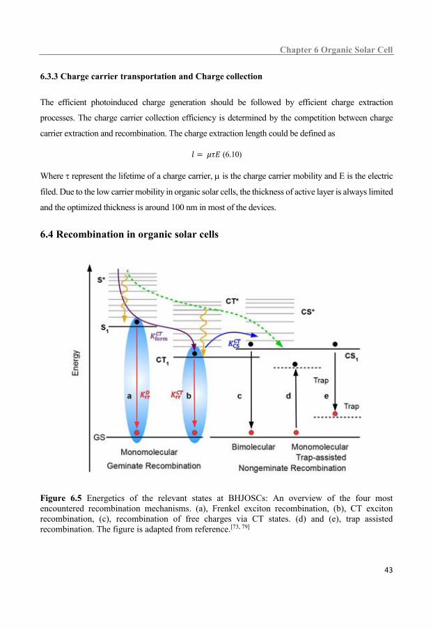
Chapter 6 Organic Solar Cell
43
6.3.3 Charge carrier transportation and Charge collection
The efficient photoinduced charge generation should be followed by efficient charge extraction
processes. The charge carrier collection efficiency is determined by the competition between charge
carrier extraction and recombination. The charge extraction length could be defined as
𝑙 = 𝜇𝜏𝐸 (6.10)
Where represent the lifetime of a charge carrier, is the charge carrier mobility and E is the electric
filed. Due to the low carrier mobility in organic solar cells, the thickness of active layer is always limited
and the optimized thickness is around 100 nm in most of the devices.
6.4 Recombination in organic solar cells
Figure 6.5 Energetics of the relevant states at BHJOSCs: An overview of the four most encountered recombination mechanisms. (a), Frenkel exciton recombination, (b), CT exciton recombination, (c), recombination of free charges via CT states. (d) and (e), trap assisted recombination. The figure is adapted from reference.[73, 79]
Chapter 6 Organic Solar Cell
44
The ideally scenario is that every absorbed photon is successfully converted into the free charge
carriers and collected at electrodes. While the reality is that each step described above from photo
absorption to charge collection is wrought with potential loss mechanism limiting the power
conversion efficiency of the organic solar cells. The involved different kinds of recombination in
the photovoltaic process are summarized in Figure 6.5.
6.4.1 Geminate recombination
Geminate recombination means that the recombination involving an electron-hole pair originates
from a single photon event. The geminate recombination include the losses of excitons that relax
to the ground state before they dissociate to CT excitons at D/A interface and the losses of CT
excitons relaxation before dissociating to free charge carriers. Both of these two kinds of geminate
recombination are considered as monomolecular recombination.
6.4.2 Non-geminate recombination
During the extraction process of free charge carriers, the free charge carriers could be eliminated
via non-geminate recombination. Non-geminate recombination includes three different kinds of
mechanisms. They are bimolecular recombination, trap-assistant recombination and auger.
Bimolecular recombination
Bimolecular recombination also named Langevin recombination means the recombination of free
holes and free electrons originating from different excitons. The recombination rate of Langevin
recombination follows the formula
𝑅𝐿 = 𝑞
𝜀(𝜇𝑛 + 𝜇𝑝 )(𝑛𝑝 − 𝑛𝑖
2), (6.11)
Where is Langvin-reduction factor for the net recombination, q the elementary charge, the
dielectric constant, and μn and μp are the mobility of electrons and holes respectively. n and p
represent the electron and hole charge density respectively and ni is the intrinsic carrier
concentration. Bimolecular recombination mainly happens at the D/A interface via CT state,
confirmed by EL from injected charges at low voltage radiative decay through CT state in some
Chapter 6 Organic Solar Cell
45
system. So decreasing of D/A interface area would reduce the probability of opposing charge
carriers finding one another thereby suppressing bimolecular recombination.
Trap assisted recombination
Trap assisted recombination, processes d and e in Figure 6.5, is a process where free carriers
recombine with the trapped opposite carriers resident in trap states. Trap assisted recombination
includes two steps, typically one carrier first is captured by a trap state and then the second opposite
free charge carrier recombines with trapped carriers. Although two charge carriers are involved in
trap assisted recombination, it is monomolecular recombination because just one carrier is involved
at a time. The Shockley-Read-Hall recombination model describing trap assisted recombination in
inorganic semiconductors can be applied to organic solar cell and the recombination rate is then
expressed by the formula [80]
𝑅𝑆𝑅𝐻 = 𝐶𝑛𝐶𝑝𝑁𝑡𝑟(𝑛𝑝 − 𝑛𝑖
2)
𝐶𝑛(𝑛 + 𝑛1)𝐶𝑝(𝑃 − 𝑃1), (6.12)
Trap assisted recombination usually originates from impurities in organic semiconductors, creating
energy levels inside the forbidden band gap. In this thesis, one kind of trap assisted recombination
is caused by ICT states formed at the interface of donor and acceptor.[9, 43, 72]
6.4.3 Distinguishing of bimolecular recombination and monomolecular recombination.
Generally speaking, under open-circuit conditions, the dominant recombination can be
distinguished from the dependence of Voc on the natural logarithm of the light intensity.
Monomolecular dominant recombination has a slope of 2.0 kT/e, while bimolecular dominant
recombination has a slope of kT/e.
6.4.4 Voltage losses in organic solar cell
Two definitions of the voltage losses are used in this thesis, both commonly used in literature. One
way is to relate the measured Voc to the electrical (transport) gap, and the other way is to compare
the measured Voc with the optical gap.[81] The electrical gap is defined as the difference in energies

Chapter 6 Organic Solar Cell
46
of the states that are occupied by free electrons and free holes. The optical gap of the devices is
defined as the minimum of the optical gaps of the donor and acceptor materials.
An empirical estimate of the Voc in terms of the HOMO of the donor and the LUMO of the acceptor
was proposed without considering vacuum level misalignment as shown in equation 6.13[16]
𝑉𝑜𝑐 = (−|𝐸𝐻𝑂𝑀𝑂𝐷 | + |𝐸𝐿𝑈𝑀𝑂
𝐴 |)𝑞−1 − 0.3𝑉, (6.13)
Where 0.3V is an empirical value, representing losses of Voc compared to the electrical gap, i.e.
differences between HOMO of the donor and LUMO of the acceptor (EA LUMO – ED
HOMO). The value of
the HOMO and LUMO are estimated from the oxidation/reduction potential measured by
electrochemical method.
As discussed in chapter 4, The IP and EA can be measured via UPS and IPES respectively, so the
electrical gap can be expressed as
∆𝐸𝑔𝐷𝐴 = 𝐼𝑃𝐷 − 𝐸𝐴𝐴, (6.14)
There can be spontaneous integer charge transfer when organic materials are brought into contact
and the integer charge transfer energy can be used to predict the organic/organic interface
interaction and energy-level alignment as we discussed in chapter 4.[2, 34, 41, 42] In organic solar cell,
when the EICT- of the acceptor is larger than the EICT+ of the donor, there should be charge transfer
between donor and acceptor in the dark ground state and formation of the dipole at the interface,
creating a vacuum level misalignment. In that case, the effective electrical gap can be reformulated
as
∆𝐸𝑔,𝑒𝑓𝑓𝐷𝐴 = 𝐼𝑃𝐷 − 𝐸𝐴𝐴 + ∆, (6.15)
Where represents interface potential step obtained from difference between acceptor EICT- and
donor EICT+
∆= |𝐸𝐼𝐶𝑇+,𝐷 − 𝐸𝐼𝐶𝑇−,𝐴|, (6.16)
At open circuit voltage, the generation rate of the free charge carriers should equal to the
recombination rate. The recombination occurs mainly through direct bimolecular recombination
and trap assisted recombination in the good contact devices. The occupied ICT states can act as

Chapter 6 Organic Solar Cell
47
sites for trap assisted recombination. Two extreme situations is sole bimolecular recombination
and sole trap assisted recombination, respectively. The Voc under each situation can be expressed
as equation 6.17 and 6.18.
𝑒𝑉𝑜𝑐 = 𝐸𝑔,𝑒𝑓𝑓𝐷𝐴 − 𝑘𝐵𝑇𝑙𝑛
𝑁𝑐𝑁𝑣
𝐺 𝛽⁄, (6.17)
𝑒𝑉𝑜𝑐 = 𝐸𝑔,𝑒𝑓𝑓𝐷𝐴 − 2𝑘𝐵𝑇𝑙𝑛
𝛽𝑅𝑆𝐻𝑁𝐼𝐶𝑇√𝑁𝐶𝑁𝑉
𝐺, (6.18)
Where G is the generation rate, and NC/NV is the effective states. /RSH represents bimolecular/trap
assisted recombination coefficient respectively. More general equation can be reformed to equation
6.19.
𝑒𝑉𝑜𝑐 = 𝐸𝑔,𝑒𝑓𝑓𝐷𝐴 − 𝑛𝑠𝑘𝐵𝑇𝑙𝑛
𝛽𝑁𝑐𝑁𝑣 + 𝛽𝑅𝑆𝐻𝑁𝐼𝐶𝑇√𝑁𝐶𝑁𝑉𝑒𝑥𝑝 (∆𝐸𝑔,𝑒𝑓𝑓
𝐷𝐴 − 𝑒𝑉𝑂𝐶
2𝑘𝑇)
𝐺
≈ 𝐸𝑔,𝑒𝑓𝑓𝐷𝐴 − 𝑛𝑠𝑘𝐵𝑇𝑙𝑛 (
𝐶0 (∆)
𝐺) (6.19)
Voc loss is here defined as the deviation from the effective electrical gap (EDA g, eff), i.e. ideal Voc, in
the measured Voc, which can be formulated as
𝑉𝑜𝑐 𝑙𝑜𝑠𝑠 = ∆𝐸𝑔,𝑒𝑓𝑓𝐷𝐴 𝑞−1 − 𝑉𝑜𝑐, (6.20)
Insert equation 6.20 to equation 6.17 and 6.18, Voc loss can be expressed as equation 6.21 and
6.22.[43]
𝑒𝑉𝑜𝑐 𝑙𝑜𝑠𝑠 = 𝑘𝐵𝑇𝑙𝑛𝑁𝑐𝑁𝑣
𝐺 𝛽⁄, 𝐸𝐼𝐶𝑇+ > 𝐸𝐼𝐶𝑇−, (6.21)
𝑒𝑉𝑜𝑐 𝑙𝑜𝑠𝑠 = 𝑛𝑠𝑘𝐵𝑇𝑙𝑛 (𝐶0 (∆)
𝐺) , 𝐸𝐼𝐶𝑇+ < 𝐸𝐼𝐶𝑇−, (6.22)

Chapter 6 Organic Solar Cell
48
Occupied integer charge transfer states at the donor/acceptor (D/A) interface, occurring when EICT+,
D ≤ EICT−, A (Figure 1), can act as trap sites for recombination that reduce the Voc, while the
generation of free charges at the D/A interface is enhanced by the interface potential energy
gradient generated by occupied integer charge transfer states. Hence, there is a trade-off in terms
of occupied integer charge transfer state density and the sweet spot occurs at EICT+ EICT- as shown
in Figure 6.6.
Figure6.6 Voc loss versus EICT+, D – EICT-, A for a series of polymer: fullerene. eVoc loss = EDA g, eff – eVoc.
The green region contains the polymer: fullerene blends where EICT+, D EICT−, A within the error bar of the measurement. The figure is adapted from reference.[15]
When the measured Voc is compared to optical gap, the Voc,loss can be expressed by the formula
𝑉𝑜𝑐,𝑙𝑜𝑠𝑠 = 𝐸𝐷∗𝑞−1 − 𝑉𝑜𝑐 (6.23)
Where ED* is the optical gap that could be determined from the cross point of the normalized
absorption and emission spectra as shown in Figure A1 or usually extracted directly from the onset
of the absorption spectra.[69, 72, 82] Before charge generation, the strongly bound excitons in the neat

Chapter 6 Organic Solar Cell
49
donor/acceptor materials need convert into delocalized charge transfer states. The voltage losses
can be divided into two parts, charge transfer losses and recombination losses, and the equation
6.23 can be rewritten as
𝑉𝑜𝑐,𝑙𝑜𝑠𝑠 = (𝐸𝐷∗ − 𝐸CT)𝑞−1 + (𝐸CT𝑞−1 − 𝑉𝑜𝑐), (6.24)
Where (ED* – ECT) is defined as driving force. The generation rate of the free charge carriers should
be equal to the recombination rate at open circuit condition. In other words, at Voc, the
recombination current balances with the photogenerated current and Voc is given by equation
(6.25). Starting from which, the Voc could be related to the ECT as shown in equation (6.28). The
detailed process can be found in the literature.
𝑉𝑜𝑐 = 𝑘𝑇
𝑞ln (
𝐽𝑃ℎ
𝐽0+ 1) (6.25)
Where J0 is related to electro-optical properties by formula (6.26)
𝐽0 =𝑞
𝐸𝑄𝐸𝐸𝐿∫ 𝐸𝑄𝐸𝑃𝑉(𝐸)∅𝐵𝐵
𝑇 𝑑𝐸 (6.26)
Here, EQEEL is the electroluminescence EQE and T BB is the black body photon flux at temperature
T that can be expressed as
∅𝐵𝐵𝑇 =
2𝜋
ℎ3𝑐2𝐸2𝑒𝑥𝑝 (−
𝐸
𝑘𝑇) (6.27)
The T BB is strongly decreasing with increasing of photo energy, so only low energy CT part of the
EQEPV spectra contributes to J0. Combining formula 6.9, 6.25, 6.26, and 6.27, the Voc can be
expressed as in equation 6.28.
𝑉𝑜𝑐 = 𝐸𝐶𝑇
𝑞+
𝑘𝑇
𝑞𝑙𝑛 (
𝐽𝑠𝑐𝑐2ℎ3
𝑓𝑞2𝜋(𝐸𝐶𝑇 − )) +
𝑘𝑇
𝑞𝑙𝑛(𝐸𝑄𝐸𝐸𝐿), (6.28)
When the ECT is considered as the effective optical bandgap, the Voc losses compared to ECT can be
reformulated as equation (6.29)

Chapter 6 Organic Solar Cell
50
𝑉𝑜𝑐,𝑙𝑜𝑠𝑠𝑒 = (𝐸CT𝑞−1 − 𝑉𝑜𝑐)
=−𝑘𝑇
𝑞𝑙𝑛 (
𝐽𝑠𝑐𝑐2ℎ3
𝑓𝑞2𝜋(𝐸𝐶𝑇 − )) +
−𝑘𝑇
𝑞𝑙𝑛(𝐸𝑄𝐸𝐸𝐿) (6.28)
= ∆𝑉𝑟𝑎𝑑 + ∆𝑉𝑛𝑟𝑎𝑑 (6.29)
Where voltage losses are divided into radiative (ΔVrad) and non-radiative (ΔVnonrad) recombination.
The radiative energy losses are in principle unavoidable, since any light absorber should also emit
light. If caused by defects and impurities, non-radiative recombination is avoidable, resulting in a
maximum Voc if the electroluminescence external quantum efficiency (EQEEL) is close to 1. When
there is only radiative recombination, the Voc,rad could be expressed as equation 6.30
𝑉𝑜𝑐,𝑟𝑎𝑑 = 𝐸𝐶𝑇
𝑞+
𝑘𝑇
𝑞𝑙𝑛 (
𝐽𝑠𝑐𝑐2ℎ3
𝑓𝑞2𝜋(𝐸𝐶𝑇 − )) (6.30)
The relationship of the recombination current and voltage in equation 6.25 can be reformulated as
equation 6.31 if there are only radiative recombination.
𝑉𝑜𝑐,𝑟𝑎𝑑 = 𝑘𝑇
𝑞ln (
𝐽𝑃ℎ
𝐽0,𝑟𝑎𝑑+ 1) (6.31)
Where J0,rad can be got from equation 6.32
𝐽0,𝑟𝑎𝑑 = 𝑞 ∫ ∅𝑒𝑚
∞
0
(𝐸, 𝑉 = 0)𝑑𝐸 = ∫ 𝐸𝑄𝐸𝑃𝑉
∞
0
(𝐸)∅𝐵𝐵(𝐸)𝑑𝐸 (6.32)
∆𝑉𝑜𝑐,𝑛𝑟 = 𝑉𝑜𝑐,𝑟𝑎𝑑 − 𝑉𝑜𝑐 = −𝑘𝑇
𝑞𝑙𝑛𝐸𝑄𝐸𝐸𝐿 (6.33)
Minimizing the non-radiative recombination loss can significantly improve the Voc and
performance of the organic solar cell. EQEEL for organic solar cell is typically around 10-6 to 10-9,
which counts for a high voltage loss around 0.3–0.6 V compared to inorganic solar cell and
perovskite solar cells. The inorganic solar cells have the lowest ΔVnr in the range of 0.04–0.21 V.[83]
For Perovskite solar cells, it is around 0.2–0.5 V.[83] It has been proved recently that the Voc, nr can

Chapter 6 Organic Solar Cell
51
be decreased to around 0.24V in both fullerene (Figure 6.7)[72] and non-fullerene system that
contribute significantly to enhance the open circuit voltage in organic solar cells.[84]
Figure 6.7 (a) EQEEL spectra and (b) FTPS-EQE spectra of the PIDTT-TID: PC71BM (1:3)
blend. The figures were adapted from reference.[72]

Chapter 6 Organic Solar Cell
52

Chapter 7 Ternary Organic Solar Cell
53
Chapter 7 Ternary Organic Solar Cell
7.1 Advantages of ternary organic solar cells
Improvement of any steps involved in working process of organic solar cells from photo absorption
to charge collection would afford probability of improving the performance of organic solar cells.
New donor materials, non-fullerene acceptors and developments in electrode design have
pushed the power conversion efficiency (PCE) of the binary donor/acceptor (D/A) BHJOSC
to over 12% by improving photon harvesting ability, charge generation, charge transport
and/or charge extraction. So-called tandem and ternary device structures also have been
deployed to enhance PCE. Both concepts use an additional absorbing material (donor or
acceptor) to extend the spectral range of light absorption, but the tandem approach uses two
stacked binary sub-cells that covers different parts of the solar spectrum, which is
significantly harder to fabricate in a printing process and requires current matching between
the two sub-cells, in practice limiting the device to the lower-current sub-cell, whereas the
ternary approach uses a single absorbing layer compromising three organic semiconductors:
two donors and one acceptor (D1/D2/A) or two acceptors and one donor (D/A1/A2) to
achieve improved coverage of the solar spectrum that retains the simplicity of printing
process from the binary D/A bulk-heterojunction solar cells. Besides of the expanded
coverage of the solar spectrum and access to easy solution processing mentioned above,
ternary organic solar cells can improve the charge dissociation and transportation, and as
we now show in this thesis, the Voc can also be enhanced.
Although there are various advantages for ternary organic solar cells, the introduction of the
third component making the working mechanism complicate and different from binary solar
cells instead of simple superposition of the working process of referenced binary solar cells.
There are mainly three working mechanisms in a ternary solar cell: charge transfer, energy
transfer and parallel-linkage. The determining factors of working principles are the energy
level alignment of the three components and the distribution of the third component in the
active layer. The third component could be locate at the D/A interface, or embedded in
donor or acceptor, or form their own channels as shown in Figure7.1.

Chapter 7 Ternary Organic Solar Cell
54
Figure7.1 Working mechanism of ternary organic solar cell. The third component (a) locates at the interface of the host donor and acceptor, and (b) and (c) embeds in host acceptor or donor, and (d) forms its own channel.
7.2 Distribution of the third component and identification methods
Distribution of the third component in ternary blend includes two aspects. One is the vertical
distribution of the third component, and another is the location of the third component
relative to host binary blend in ternary blend films, both of which are important for ternary
solar cells. The energy levels and energy level alignment can be determined via CV or UPS
measurement as we discussed earlier. The vertical distribution can be measured by e.g.
photoelectron spectroscopy (UPS and XPS) and both of the vertical distribution and the
location of the third component in the ternary blend can be identified via contact angle
measurements.

Chapter 7 Ternary Organic Solar Cell
55
The frontier electronic structure is unique for a specific material so the UPS spectra will be different
from each other, especially in the region of the frontier orbitals. The UPS spectra of the neat film
and the blend film then can be measured to identify the vertical distribution according to the shape
of the valence band as shown in Figure7.2. The major component at the surface can be identified
by comparing the properties of frontier orbital of pure and blend film in UPS spectra, and the ratio
of each component can be obtained by fitting the UPS spectra. More accurate quantitative
measurement can be done via XPS measurements. The ratio of each component can be deduced
via calculating the ratio of the featured elements in each material.[85]
Figure 7.2 Valence band structure of neat PTB7-Th, m-ITIC and blends obtained from UPS spectra. Adapted from reference.[9]
Another simple method is the contact angle measurement as shown in Figure 7.3. The surface
energy here can be deduced from the contact angle. The materials with the lower surface energy
(large contact angle) will tend to be segregated into the air/film interface while the material with
higher surface energy (small contact angle) typically is going to be segregated to the film/electrode
interface.
Figure7.3 Water contact angle of three different films, PC71BM (left), m-ITIC (middle), PTB7-Th (right). Adapted from reference.[9]

Chapter 7 Ternary Organic Solar Cell
56
As to the location of the third component in the blend, it can be determined via wetting coefficient
calculation of each component according to the measured contact angle. The wetting coefficient of
the third component in blends of materials donor A and acceptor C can be calculated according to
Equation 7.1 (Young’s equation according), where s(c) represents the wetting coefficient and
s(X)s(Y) represents the interface surface energy between solid X and solid Y, which can be deduced
from Equation 7.2 (Neumann’s equation).sv represent surface tension energy between solid(s) and
vapor (v), which can be deduced from Equation 7.3 and lv represent liquid-vapor surface tension.
represents the water contact angle of the film. is 0.000115 m4mj-2 in Equation 7.2 and 7.6. The
physical meaning and detail derivation process of each equation can be found in literature. When
s(C) -1, the third component C will tend to embed in the domain of material Acceptor C.
s(C) 1, the third component will tend to embed in the domain of material Donor A.
-1 s(C) 1, the third component will tend to distribute at the interface of Donor A and acceptor
C.
𝜔𝑠(𝐶) =𝛾𝑠(𝐶)𝑠(𝐵) − 𝛾𝑠(𝐶)𝑠(𝐴)
𝛾𝑠(𝐴)𝑠(𝐵), (7.1)
𝛾𝑠(𝑋)𝑠(𝑌) = 𝛾𝑠(𝑋)𝑣 − 𝛾𝑠(𝑌)𝑣 − √(𝛾𝑠(𝑋)𝑣𝛾𝑠(𝑌)𝑣) ∗ 𝑒𝑥𝑝 (−𝛽(𝛾𝑠(𝑋)𝑣𝛾𝑠(𝑌)𝑣)2
) , (7.2)
𝛾𝑠𝑣 = 𝛾𝑙𝑣𝑥𝑛+12 , (7.3)
𝑥𝑛+1 = 𝑥𝑛 −𝑥𝑛 − 𝑎𝑒𝑏(1−𝑥𝑛
2)2
1 + 4𝑎𝑏𝑥𝑛 (1 − (𝑥𝑛2)𝑒𝑏(1−𝑥𝑛
2)2
) (0 ≤ 𝑥 ≤ 1), (7.4)
𝛼 =cos 𝜃 + 1
2, (7.5)
𝑏 = 𝛽𝛾𝑙𝑣2 , (7.6)

Chapter 7 Ternary Organic Solar Cell
57
7.3 Working mechanisms of ternary organic solar cells
There are mainly three kinds of working mechanisms in ternary solar cells, as mentioned, which is
determined by the relative energy levels and the distribution of each component. They are charge
transfer, energy transfer and parallel linkage respectively. In many ternary solar cells, all these
mechanisms usually coexist with one dominate process.[86, 87] Different kinds of working
mechanisms could be identified via PL and J-V curve measurement.
7.3.1 Cascade exciton dissociation and charge transfer
Figure 7.4 Cascade charge transfer mechanism
During design process of ternary solar cells with charge transfer and transport as dominate
mechanisms, the selection of the third component should meet the two main requirements. The first
one is that the third component should locate at the interface of the dominant donor and acceptor
so as to form a percolating pathway for charge transfer and transportation, and the second one is
that the energy levels of the third component should locate between the energy levels of the host
donor and acceptor, as shown in Figure7.4, forming a “cascade junction”. The charge transfer
mechanism is that there is exciton dissociation and charge transfer between two donors (D1/D2) or
two acceptors (A1/A2) in addition of the exciton dissociation and charge transfer at the interface
of donor and acceptor (D/A) similar to that in binary solar cell. In double donor ternary, the excitons
generated in donor D1 can transfer electrons to either acceptor A or donor D2. In the latter case,
the D2 subsequently transfers electrons to the acceptor A. While the excitons generated in D2 can

Chapter 7 Ternary Organic Solar Cell
58
transfer the electron to acceptor and in parallel the hole to D1. Following the charge transfer, the
electrons are transported to cathode through the channel formed by the acceptor domains and the
holes are transported to anode through the channel formed by the host donor. Similar process can
occur in double acceptor ternary system, the excitons generated in acceptor A2 can transfer a hole
either to donor D or acceptor A1. In the latter case, the acceptor A1 subsequently transfers a hole
to the donor D. Alternatively the excitons generated in acceptor A1 could transfer a hole to donor
D and in parallel the electron to A2. The electrons are transported to the cathode through the
channel formed by host acceptor A2 and the holes are transported to anode through the channel
formed by donor. The charge transfer between two donors or two acceptors can be measured by J-
V curves. If there is charge transfer between two donors or two acceptors, composing a solar cell
device, the blend device usually shows larger Jsc and medium Voc compared to the corresponding
neat film devices as shown in Figure 7.4. Another convenient method is the PL measurement. If
there is charge transfer between two donors (or two acceptors), the PL emission intensity of one
donor (acceptor) would be reduced without increasing PL intensity of other donor (acceptor). TRPL
combined with the optical gap can also afford proof of charge transfer.
Figure7.4 J-V curves of two donor polymers and their blend with the ration of 1:1.
The electrons and holes are mainly transported to the electrodes through the channels formed by
the host acceptor and donor, respectively, so the loading of the third component at the interface of
the host donor and acceptor would decrease the probability that electrons and holes to meet and
recombine, so the voltage losses due to CT state recombination can be decreased.[88, 89] The trap

Chapter 7 Ternary Organic Solar Cell
59
assisted recombination via ICT states can also be tuned by addition of the third component at the
interface of the host donor and acceptor.[9]
7.3.2 Energy transfer
Figure 7.5 Energy level diagram in ternary blend with energy transfer mechanism.
Energy transfer between two donors or two acceptors is a competing process compared with charge
transfer in ternary blend films as shown in Figure 7.5. In addition to the advantages of the ternary
solar cell we mentioned, the energy transfer has the potential to improve the efficiency of the solar
cell, even surpassing the Shockley-Queisser (S-Q) limit of a single p-n junction. Two strategies in
conjugation with the energy transfer mechanism are singlet fission and upconversion.[90, 91, 92]
During energy transfer, an exciton can be relocated from excited energy donor to an energy
acceptor via non-radiative process. The non-radiative energy transfer process requires that the
energy of the energy donor excited state must be higher than that of the energy acceptor excited
state and the energy transfer rate must he faster than the intrinsic decay rate of the excited energy
donor. At the end of energy transfer process, the energy donor is in the ground state and the energy
acceptor is in the excited state. The energy transfer mechanisms include two types of mechanisms:
Förster energy transfer and Dexter energy transfer. Förster energy transfer is based on a dipole-
dipole electromagnetic interaction and requires that the absorption spectrum of energy acceptor
should overlap with the emission spectrum of energy donor completely or partially at least as
shown in Figure 7.6. Förster energy transfer occurs through space via electromagnetic interaction
and can therefore occur over long distance, typically around 1-5 nm. The efficiency of the Förster

Chapter 7 Ternary Organic Solar Cell
60
energy transfer decreases with the distance between energy donor and energy acceptor as r-6
(equation 7.7)
𝐾𝐸𝑇 = 1
𝜏𝐷(
𝑅𝑐
𝑟)
6
, (7.7)
Where D is the life time of the excited states of the energy donor, and r is the distance between
energy donor and energy acceptor. Rc is the critical radius and represent the distance at which the
energy transfer rate is equal to the intrinsic decay rate of the donor.
Figure 7.6 Normalized emission spectrum of energy donor and absorption spectrum of energy
acceptor. Adapted from the reference.[15]
Dexter energy transfer needs an overlap of the wavefunctions between energy donor and energy
acceptor so as to allow electron exchange. Hence it just can take place over short distances,
typically around 1.0 nm. The rate of Dexter energy transfer exponentially decreases with the
distance between energy donor and energy acceptor (equation 7.8).
𝐾𝐸𝑇 = 𝐾𝐽𝑒𝑥𝑝 (−2𝑟
𝐿) , (7.8)
Where k is related to the specific orbital interactions and r is the donor acceptor separation. L is the
sum of the van der Vaals radii and J is the normalized spectral overlap integral.

Chapter 7 Ternary Organic Solar Cell
61
In a ternary system, when the third component act as energy acceptor, D2 in double donor system
and A2 in double acceptor system as shown in Figure 7.5, it should be adjacent both to the energy
donor D1 or A1 and host acceptor D or host donor A. When the third component act as energy
donor, D1 in double donor system and A1 in double acceptor system as shown in Figure 7.5, the
third component just need but have to adjacent to the energy acceptor D2 or A2 due to the limited
radius of energy transfer. In a double donor ternary system involving energy transfer, the exciton
energy in D1 can be transferred to D2 and the excitons generated in D2 dissociated at the D2/A
interface. The hole would be transported to the anode directly or transferred to D1 then transported
to the anode, while the electrons are transported to cathode (mainly) via the acceptor. In double
acceptor system, the excitons generated in A1 can be energy transferred to A2 and then dissociated
at the D/A2 interface. The hole can be transferred to the anode via D and the electrons are
transported to the cathode directly or transferred to A1 then transported to the cathode. The energy
transfer can be identified by PL measurements. The PL intensity quenching of the energy donor
will increase the PL intensity of the energy acceptor as shown in the Figure 7.6.
Figure7.6 PL spectra involving energy transfer. PTB7-Th act as energy acceptor and PBDTTS-
FTAZ act as energy donor. The figure is adapted from reference.[15]
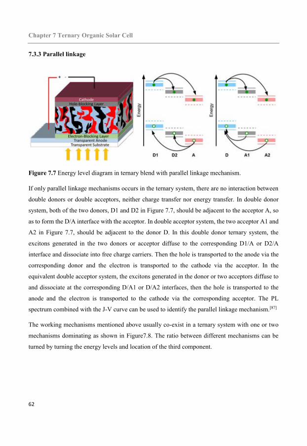
Chapter 7 Ternary Organic Solar Cell
62
7.3.3 Parallel linkage
Figure 7.7 Energy level diagram in ternary blend with parallel linkage mechanism.
If only parallel linkage mechanisms occurs in the ternary system, there are no interaction between
double donors or double acceptors, neither charge transfer nor energy transfer. In double donor
system, both of the two donors, D1 and D2 in Figure 7.7, should be adjacent to the acceptor A, so
as to form the D/A interface with the acceptor. In double acceptor system, the two acceptor A1 and
A2 in Figure 7.7, should be adjacent to the donor D. In this double donor ternary system, the
excitons generated in the two donors or acceptor diffuse to the corresponding D1/A or D2/A
interface and dissociate into free charge carriers. Then the hole is transported to the anode via the
corresponding donor and the electron is transported to the cathode via the acceptor. In the
equivalent double acceptor system, the excitons generated in the donor or two acceptors diffuse to
and dissociate at the corresponding D/A1 or D/A2 interfaces, then the hole is transported to the
anode and the electron is transported to the cathode via the corresponding acceptor. The PL
spectrum combined with the J-V curve can be used to identify the parallel linkage mechanism.[87]
The working mechanisms mentioned above usually co-exist in a ternary system with one or two
mechanisms dominating as shown in Figure7.8. The ratio between different mechanisms can be
turned by turning the energy levels and location of the third component.
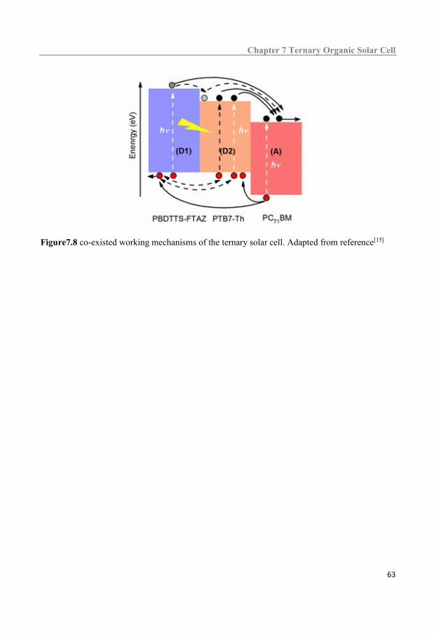
Chapter 7 Ternary Organic Solar Cell
63
Figure7.8 co-existed working mechanisms of the ternary solar cell. Adapted from reference[15]

Chapter 7 Ternary Organic Solar Cell
64
Chapter 8 Stability of Organic Solar Cell
65
Chapter 8 Stability of Organic Solar Cell
8.1 Parameters impacting the stability of organic solar cells
Solution processing of organic molecules/polymers allows for low-temperature manufacturing of
organic photovoltaics on flexible substrates using common printing techniques, which affords a
promising route for the realization of low-cost, large area, flexible and light weight organic solar
cells with shorter energy payback time. On the other hand, the relative low efficiency compared to
inorganic solar cell and inferior stability are so far hindering the commercialization of the organic
solar cell. The efficiency of the organic solar cell has been pushed to over 12% in recent years by
various strategies, such as designing and synthesizing new active layer and interface layer materials,
designing and fabricating ternary and tandem solar cells, etc. The overall stability of an organic
solar cell is affected by the stability of each component, such as the stability of the electrode,
interface layer and active layer.
The active layer containing the conjugated molecules/polymers is the key component of an organic
solar cell, but these molecules/polymers generally suffer from poor air stability and require an inert
atmosphere processing environment, which increases manufacturing complexity and cost. Thus,
understanding of the stability and degradation mechanism is another key issue. The factors leading
to degradation of the conjugated molecules/polymers mainly include oxygen, water, heating,
illumination and diffusion of the interface layer and electrodes. All these factors are often coupled
with each other at the same time and the degradation of conjugated molecules/polymers typically
follow many complicated pathways. Therefore, it’s necessary to figure out the effect of each
parameter responsible for the degradation so as to find out the corresponding strategies to prevent
the degradation of the active layer and increase the stability of the organic solar cell. Photoelectron
spectroscopy provides a convenient in-situ method of studying the degradation of conjugated
molecules/polymers by controlling exposure of oxygen and water vapor separately.
8.2 In-situ method of studying degradation
Photo electron spectroscopy is a powerful technique to measure the frontier electronic structure
and interface properties of thin films.[2, 93, 94] The detrimental changes in the frontier electronic
Chapter 8 Stability of Organic Solar Cell
66
structure and interface properties caused by various factors such as oxygen, water, heating and
illumination can be probed.[95, 96, 97, 98] An advantage of this method is that the exposure of oxygen
and water can be separately monitored quantitatively. The active layer of an organic solar cell is
composed by both p-type donor and n-type acceptor. It has been proved that it’s more difficult to
develop practically useful n-type semiconductors compared to p-type semiconductors.[99, 100]
Indeed, fullerene was the dominant acceptors in organic solar cells until the recent rapid
development of the non-fullerene acceptors. Thus, in this thesis, the attention is focused on the
degradation of the n-type acceptors.
It is revealed by the in-situ method that both oxygen and water tend to interact with the fullerene
part of the PCBM. The interaction between oxygen and fullerene is a weak interaction, because the
frontier electronic structure cannot be affected except of the whole spectra shifting toward the high
binding energy and this shifting is reversible when the sample is treated by thermal annealing in
vacuum.[97] Water exposure, on the other hand, leads to significant chemical interaction as revealed
by PES where the frontier orbital in the UPS spectra are irreversibly broadened and bleached, and
new features appear in the XPS spectra.[97] The rapid development of non-fullerene acceptors in
the last two years now affords more recipes for designing both efficient and stabile OSC, as
discussed in this thesis where non-fullerene acceptors are successfully used to design ternary solar
cells with both enhanced efficiency and thermal stability. Besides improving the efficiency of the
devices, understanding of the stability and degradation mechanism of the non-fullerene acceptors
exposed to water and oxygen is obviously a key issue. Three n-type non-fullerene small molecular
acceptors are investigated in this thesis. All of them are exposed to oxygen and water vapor
separately. The experiment results reveal that the degradation mechanism of non-fullerene
acceptors is different from the fullerene acceptors, and that the non-fullerene acceptors show more
tolerance to both of water vapor and oxygen, a promising development for the technology.
8.3 Thermal stability of the active layer containing non-fullerene acceptors
Thermal stability is also crucial for organic solar cell because the working temperature of the
organic solar cell is often high due to continuous illumination during the day. It is well known that
thermal annealing of the device can lead to diffusion of metal ions from the electrodes into the
active layer and create leakage current.[101, 102] Furthermore, the high temperature can induce

Chapter 8 Stability of Organic Solar Cell
67
chemical reactions at the metal/organic interface and alter the interface (morphology) properties.[103,
104] In order to investigate the thermal stability of the active layer, the device structure of
ITO/PEDOT:PSS/active layer/ZnO/Al could be adopted because it has been proved that the
interface between active layer and electron/hole transportation layer are electronically stable during
thermal stress, which allows exclusion of thermal degradation of the interfacial layers during the
annealing of the device.[105] The experiment results in this thesis proved that incorporation of the
non-fullerene acceptor into the ternary blend strongly improves thermal stability of the solar cell
under industrial relevant thermal stress. The J-V curve in Figure 8.1 present the comparison of the
thermal stability of fullerene containing binary and non-fullerene containing ternary solar cell.
Figure 8.1 J-V curves of fresh and degraded devices for a binary solar cell and b) ternary solar cell
under simulated AM 1.5 G irradiation (100 mW cm-2). Adapted from reference.[9]

Chapter 8 Stability of Organic Solar Cell
68

Chapter 9 Summary of Papers and Further Outlook
69
Chapter 9 Summary of Papers and Further Outlook
9.1 Summary of papers
9.1.1 Paper 1
Relationship of Vertical Ionization Potential and Oxidation potential of -conjugated
molecules/polymers
Chuanfei Wang, Liangqi Ouyang, Slawomir Braun, Xianjie Liu, Mats Fahlman
(Manuscript)
A series of conjugated molecules/polymers typically used in organic solar cells were deposited in
Platinum substrates or Platinum electrode to form thin film. Then the vertical ionization potential
and oxidation potential were measured respectively by photoelectron spectroscopy and
electrochemical method. It was found that there is a linear relationship between IP and Eox with the
slop equal to unity (Figure 9.1). The relationship can be expressed as
IP = (1.03±0.14) qEox + (4.45±0.09) eV
Figure 9.1 The relationship between oxidation potential and vertical ionization potential.

Chapter 9 Summary of Papers and Further Outlook
70
Although the linear relationship with a slope of 1.0 presented is obtained from a set of -
conjugated organic molecules/polymers typically used for organic solar cells. We expect this
relationship to hold also for other non-metal organic semiconductors.

Chapter 9 Summary of Papers and Further Outlook
71
9.1.2 Paper 2
Low Band Gap Polymer Solar Cells with Minimal Voltage Losses
Chuanfei Wang, Xiaofeng Xu, Wei Zhang, Jonas Bergqvist, Yuxin Xia, Xiangyi Meng, Kim Bini,
Wei Ma, Arkady Yartsev, Koen Vandewal, Mats R Andersson, Olle Inganäs, Mats Fahlman,
Ergang Wang
Advanced Energy Materials, 2016, 6, 1600148
The relative higher voltage losses compared to optical gap is one of the main factors that limits the
performance of organic solar cells. The total voltage losses could be divided into two parts. They
are recombination losses including radiative and non-radiative recombination, and electron transfer
losses due to the conversion of the bonded excitons in neat materials into delocalized charge
transfer states at the interface. Compared to electron transfer losses and radiative recombination
losses, the non-radiative voltage losses constitute the largest part of the total voltage losses. In
organic solar cell, the non-radiative voltage losses is typically around 350 mV that corresponds to
an EQEEL of 10-6.
In paper 2, In order to obtain a solar cell with low voltage loss but high exciton dissociation
efficiency, PIDTT-TID was used as the donor to be blended with acceptor of the PC71BM because
the donor has a broad absorption but the deep HOMO level and the difference between the LUMO
of the donor and acceptor is around the 0.3eV, which should afford enough driving force for exciton
dissociation. The results proved that the voltage loss could be decreased to 490 mV by decreasing
non-radiative recombination to 240 mV in the low band gap polymer solar cell, while maintaining
the voltage as high as 1.0 V as shown in Figure9.2. The non-radiative voltage loss is comparable
with that of a perovskite solar cell.

Chapter 9 Summary of Papers and Further Outlook
72
Figure9.2 Plots of eVoc against Eg for Perovskite and organic solar cells with low Eloss or high Voc. Eg is determined from the absorption onset. The black solid line is the eVoc of 1.0 eV, the red dashed line is the eVoc = Eg − 0.5, and the red solid line is the eVoc = Eg − 0.6.

Chapter 9 Summary of Papers and Further Outlook
73
9.1.3 Paper 3
Ternary organic solar cells with enhanced open circuit voltage
Chuanfei Wang, Xiaofeng Xu, Wei Zhang, Sadok Ben Dkhil, Xiangyi Meng, Xianjie Liu, Olivier
Margeat, Arkady Yartsev, Wei Ma, Jörg Ackermann, Ergang Wang, Mats Fahlman
Nano Energy, 2017, 37, 24
Ternary organic solar cell combined the advantages of broad absorption of tandem solar cells and
simplicity of single bulk heterojunction solar cell, making it a promising strategy of improving the
performance of organic solar cell. The short circuit current density is usually improved in efficient
ternary system, while the Voc either assumes a value in between those obtained by the respective
binary solar cells or pins to the smaller value of the two.
Figure 9.3 Self-organized cascade junction of Donor/Acceptor1/Accepter (left panel) and enhanced Voc of ternary solar cell (right panel).
In paper 3, the polymer donor of PTB7-Th and acceptor PC71BM were employed as the host system
of the ternary solar cell. Because the EICT+ of PTB7-Th is equal to the EICT- of the PC71BM, which
is a design rule for efficient organic solar cell. The m-ITIC with smaller EICT- compared to EICT+ of
PTB7-Th was added to the host system. The surface tension and energy levels of m-ITIC make it
self-organize at the interface of the host donor and acceptor to form a cascade-type energy level
alignment (Figure 9.3). For the first time, the ternary solar cell with enhanced open circuit voltage
was designed and demonstarted (Figure 9.3). Both performance and thermal stability were

Chapter 9 Summary of Papers and Further Outlook
74
enhanced in the ternary solar cell. The enhanced open circuit voltage could be contributed to
decreased radiative bimolecular recombination and trap assisted recombination via integer charge
transfer state. We also show that this strategy can be generally used in other system.

Chapter 9 Summary of Papers and Further Outlook
75
9.1.4 Paper 4
Ternary Organic Solar Cells with Minimum Voltage Losses
Chuanfei Wang, Wei Zhang, Xiangyi Meng, Jonas Bergqvist, Xianjie Liu, Zewdneh Genene,
Xiaofeng Xu, Arkady Yartsev, Olle Inganäs, Wei Ma, Ergang Wang, Mats Fahlman
Advanced Energy Materials, 2017, 6, 1700390
According to integer charge transfer model, the appearance of integer charge transfer states in
organic solar cell could be the site of trap assistant recombination and increase the voltage losses
of organic solar cell, while the charge generation would be enhanced because of the existence of
the ICT state. The trade-off between charge generation and charge recombination by ICT state will
happen at EICT+ EICT-, where the voltage losses is minimized (Figure 9.5).
Figure 9.5 (a) Voc loss versus EICT+, D − EICT−, A for a series of polymer: fullerene. (b) UPS spectra of pure PTB7-Th and pure PBDTTS-FTAZ film on the substrate of ITO/PEDOT: PSS.
In paper 4, low-bandgap polymer PTB7-Th and a high-bandgap polymer PBDTTS-FTAZ sharing
the same bulk ionization potential and interface positive integer charge transfer energy while
featuring complementary absorption spectra are selected as two donors to fabricate efficient ternary
solar cells (Figure 9.4b). At the same times, the fullerene acceptor was chosen so that EICT+ of the
two donor polymers is equal to EICT- of the fullerene, enabling enhanced dissociation of all polymer
donor and fullerene acceptor excitons and suppressed bimolecular and trap assisted recombination.

Chapter 9 Summary of Papers and Further Outlook
76
It also proved that efficient energy transfer and charge transfer could coexist between the two donor
polymers with same ionization potential and positive pinning energy.
9.1.5 Paper 5
Pyrrolo 3,4-g quinoxaline-6, 8-dione-based conjugated copolymers for bulk heterojunction
solar cells with high photovoltages
Xiaofeng Xu, Chuanfei Wang, Olof Bäcke, David I James, Kim Bini, Eva Olsson, Mats R
Andersson, Mats Fahlman, Ergang Wang
Polymer Chemistry, 2015, 6, 4624
The maximum attainable voltage of the bulk heterojunction organic solar cell is determined by the
alignment of the energy levels of the donor and acceptor, i.e. the HOMO of the donor and the
LUMO of the acceptor. In order to obtain high voltage, in paper 5, four deep HOMO and medium
band gap polymers synthesized by combining electron-deficient unit PQD and electron efficient
unite PBDT and PT were used as donor in fullerene based binary organic solar cell. The experiment
shows that all of the obtained voltages for the four deep HOMO medium band gap polymers could
reach 1.0 V. The highest value is 1.08V, which is rarely observed in medium band gap polymer.

Chapter 9 Summary of Papers and Further Outlook
77
9.1.6 Paper 6
Degradation of n-type non-fullerene small molecules
Chuanfei Wang, Shaofei Ni, Slawomir Braun, Xianjie Liu, Mats Fahlman
Manuscript
Solution processing of organic molecules/polymers affords a promising route for the realization of
low-cost, large area, flexible and light weight organic solar cells with shorter energy payback time.
The relative low efficiency and inferior stability are hindering the commercialization of the organic
solar cell, however. The rapid development of the fullerene-free small molecular acceptors push
the efficiency of the organic solar cell to a higher level that if accompanied by an increased stability
may provide the needed breakthrough. So understanding the stability and degradation mechanism
of these kind of acceptors is a key issue.
In paper 6, the stability and degradation of three n-type non-fullerene small molecules, named p-
ITIC, m-ITIC and o-IDTBR, are explored via an in-situ method, employing the photoelectron
spectroscopy technique. The materials are deposited on substrates of aluminum to form thin films
and subsequently the thin films are exposed in-situ to oxygen and water respectively. The
experiment results reveal that all of the films show enhanced resistance to oxygen and water vapor
compared to fullerene small molecules. Furthermore, the evolution of the frontier orbital properties
of the non-fullerene molecules is different from the evaluation trend of the fullerene when they are
exposed to oxygen. The frontier orbital of the non-fullerene molecules are broaden and bleached
slowly with the increase of the exposure time, and the binding energy also increased slowly, while
the frontier orbital properties of fullerene in UPS spectra show no change but the binding energy
decreased quickly. More importantly, the p/m-ITIC show little degradation when exposed to water
vapor, while there is significant chemical interaction between water vapor and fullerene.

Chapter 9 Summary of Papers and Further Outlook
78
9.2 Further outlook
The experiment results in this thesis raise a lot of additional questions that need studying and
clarifying.
Besides of the IP, the determination of the EA is also an important task especially for acceptors in
organic solar cell. The usually used method in the community is electrochemical method. It is
expected that there is a liner relationship between the reduction potential Ered and the EA with the
slope equal to unit. With the rapid development of the new fullerene free acceptor materials, it’s
also urgent to determine the EA of the typically used fullerene free acceptors and extend the
relationship between the open circuit voltage losses and the pinning energy based on the established
model in fullerene solar cell.
The working mechanism of the ternary solar cell is complicated and still need to be investigated in
detail, especially the open circuit voltage of the ternary solar cell. Such as how the open circuit
voltage can be turned in ternary blend, alloy charge transfer state model or two charge transfer state
model. The alloy charge transfer model proposes that the evolution of the ECT is due to an alloy
formation when two miscible donors or acceptors are used and that the CT state can partially
delocalize. The two charge transfer state model, on the other hand, proposes that the ternary solar
cell can be viewed as comprising two separate binary solar cells and that the electrons and holes
are transported via three separated percolating networks. It should be interesting to explore how
the third component affect the open circuit voltage loss in ternary blend and a quantitative study
about the voltage loss should be conducted.
The development of polymer acceptor and fullerene-free small molecules afford more chance to
improve the performance and stability of the organic solar cell. The new acceptor materials are to
be used in ternary solar cells, such as all-polymer ternary solar cells and the ternary solar cell with
fullerene free small molecules as acceptor. The strategies used in this thesis should be tried
extending to other non-fullerene ternary systems.
One of the advantages of ternary organic solar cell is that it can be mass produced by roll to roll
methods. In the lab scale, the devices are deposited on the ITO substrate. In order to employ the
printing process and reduce the energy payback time, the ITO-free plastic substrate should be tried
to be used in the ternary devices fabrication in following research.

Chapter 9 Summary of Papers and Further Outlook
79
The electrode modifier, i.e. interface layer, can improve the charge extraction and stability of the
organic solar cell and different kinds of the buffer layer can be used in both binary and ternary solar
cell to figure out the selection principles.
The stability of the pure materials was investigated in the thesis and it is also important to figure
out the stability and the degradation mechanisms of the corresponding devices in the near future.
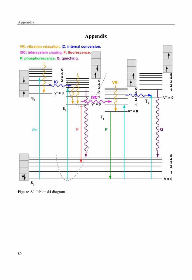
Appendix
80
Appendix
Figure A1 Jablonski diagram

Reference
81
Reference [1] C. W. Tang, S. A. Vanslyke, Appl. Phys. Lett. 1987, 51, 913. [2] S. Braun, W. R. Salaneck, M. Fahlman, Adv. Mater. 2009, 21, 1450. [3] W. N. Hansen, G. J. Hansen, Phys. Rev. A 1987, 36, 1396. [4] R. Gomer, G. Tryson, J. Chem. Phys. 1977, 66, 4413. [5] Y. Y. Liang, Y. Wu, D. Q. Feng, S. T. Tsai, H. J. Son, G. Li, L. P. Yu, J. Am. Chem.
Soc. 2009, 131, 56. [6] C. M. Cardona, W. Li, A. E. Kaifer, D. Stockdale, G. C. Bazan, Adv. Mater. 2011, 23,
2367. [7] Y. B. Cheng, A. Pascoe, F. Huang, Y. Peng, Nature 2016, 539, 488. [8] http://www.ren21.net. [9] C. F. Wang, X. F. Xu, W. Zhang, S. Ben Dkhil, X. Y. Meng, X. J. Liu, O. Margeat, A.
Yartsev, W. Ma, J. Ackermann, E. G. Wang, M. Fahlman, Nano Energy 2017, 37, 24. [10] www.ise.fraunhofer.de. [11] S. Kato, Theor. Chem. Acc. 2000, 103, 219. [12] W. R. Salaneck, Phys. Rev. Lett. 1978, 40, 60. [13] M. Campoy-Quiles, T. Ferenczi, T. Agostinelli, P. G. Etchegoin, Y. Kim, T. D.
Anthopoulos, P. N. Stavrinou, D. D. C. Bradley, J. Nelson, Nat. Mater. 2008, 7, 158. [14] A. Atxabal, S. Braun, T. Arnold, X. N. Sun, S. Parui, X. J. Liu, C. Gozalvez, R. Llopis,
A. Mateo-Alonso, F. Casanova, F. Ortmann, M. Fahlman, L. E. Hueso, Adv. Mater. 2017, 29, 1606901.
[15] C. Wang, W. Zhang, X. Meng, J. Bergqvist, X. Liu, Z. Genene, X. Xu, A. Yartsev, O. Inganäs, W. Ma, E. Wang, M. Fahlman, Adv. Energy Mater. 2017, 1700390.
[16] M. C. Scharber, D. Wuhlbacher, M. Koppe, P. Denk, C. Waldauf, A. J. Heeger, C. L. Brabec, Adv. Mater. 2006, 18, 789.
[17] H. Ishii, K. Sugiyama, E. Ito, K. Seki, Adv. Mater. 1999, 11, 605. [18] B. A. Jones, A. Facchetti, M. R. Wasielewski, T. J. Marks, J. Am. Chem. Soc. 2007, 129,
15259. [19] H. T. Nicolai, M. Kuik, G. A. H. Wetzelaer, B. de Boer, C. Campbell, C. Risko, J. L.
Bredas, P. W. M. Blom, Nat. Mater. 2012, 11, 882. [20] D. Abbaszadeh, A. Kunz, G. A. H. Wetzelaer, J. J. Michels, N. I. Craciun, K. Koynov,
I. Lieberwirth, P. W. M. Blom, Nat. Mater. 2016, 15, 628. [21] A. Pron, P. Gawrys, M. Zagorska, D. Djurado, R. Demadrille, Chem. Soc. Rev. 2010,
39, 2577. [22] P. I. Djurovich, E. I. Mayo, S. R. Forrest, M. E. Thompson, Org. Electron. 2009, 10,
515. [23] I. G. Hill, A. Kahn, Z. G. Soos, R. A. Pascal, Chem. Phys. Lett. 2000, 327, 181. [24] S. J. Yang, P. Olishevski, M. Kertesz, Synth. Met. 2004, 141, 171. [25] S. van Reenen, S. Kouijzer, R. A. J. Janssen, M. M. Wienk, M. Kemerink, Adv. Mater.
Interfaces 2014, 1, 1400189. [26] C. Arantes, M. Scholz, R. Schmidt, V. Dehm, M. L. M. Rocco, A. Scholl, F. Reinert, F.
Wurthner, Appl. Phys. A-Mater. Sci. Process. 2012, 108, 629. [27] N. D. Lang, W. Kohn, Phys. Rev. B 1971, 3, 1215. [28] N. D. Lang, W. Kohn, Phys. Rev. B 1973, 7, 3541. [29] N. D. Lang, Phys. Rev. Lett. 1981, 46, 842. [30] Y. C. Chen, J. E. Cunningham, C. P. Flynn, Phys. Rev. B 1984, 30, 7317. [31] C. Tengstedt, W. Osikowicz, W. R. Salaneck, I. D. Parker, C. H. Hsu, M. Fahlman, Appl.
Phys. Lett. 2006, 88, 053502.

Reference
82
[32] M. Fahlman, A. Crispin, X. Crispin, S. K. M. Henze, M. P. de Jong, W. Osikowicz, C. Tengstedt, W. R. Salaneck, J. Phys.-Condes. Matter 2007, 19, 183202.
[33] H. Vazquez, F. Flores, A. Kahn, Org. Electron. 2007, 8, 241. [34] S. Braun, M. P. de Jong, W. Osikowicz, W. R. Salaneck, Appl. Phys. Lett. 2007, 91,
202108. [35] X. Crispin, V. Geskin, A. Crispin, J. Cornil, R. Lazzaroni, W. R. Salaneck, J. L. Bredas,
J. Am. Chem. Soc. 2002, 124, 8131. [36] J. Chen, M. A. Reed, A. M. Rawlett, J. M. Tour, Science 1999, 286, 1550. [37] G. Heimel, L. Romaner, E. Zojer, J. L. Bredas, Accounts Chem. Res. 2008, 41, 721. [38] M. Fahlman, P. Sehati, W. Osikowicz, S. Braun, M. P. de Jong, G. Brocks, J. Electron
Spectrosc. Relat. 2013, 190, 33. [39] M. Bokdam, D. Cakir, G. Brocks, Appl. Phys. Lett. 2011, 98, 113303. [40] H. Aarnio, P. Sehati, S. Braun, M. Nyman, M. P. de Jong, M. Fahlman, R. Osterbacka,
Adv. Energy Mater. 2011, 1, 792. [41] W. Osikowicz, M. P. de Jong, W. R. Salaneck, Adv. Mater. 2007, 19, 4213. [42] R. J. Murdey, W. R. Salaneck, Jpn. J. Appl. Phys. 2005, 44, 3751. [43] Q. Y. Bao, O. Sandberg, D. Dagnelund, S. Sanden, S. Braun, H. Aarnio, X. J. Liu, W.
M. M. Chen, R. Osterbacka, M. Fahlman, Adv. Funct. Mater. 2014, 24, 6309. [44] V. I. Arkhipov, P. Heremans, H. Bassler, Appl. Phys. Lett. 2003, 82, 4605. [45] J. Isaksson, C. Tengstedt, M. Fahlman, N. Robinson, M. Berggren, Adv. Mater. 2004,
16, 316. [46] Z. Tang, W. Tress, Q. Y. Bao, M. J. Jafari, J. Bergqvist, T. Ederth, M. R. Andersson, O.
Inganas, Adv. Energy Mater. 2014, 4, 1400643. [47] Z. F. Ma, Z. Tang, E. G. Wang, M. R. Andersson, O. Inganas, F. L. Zhang, J. Phys.
Chem. C 2012, 116, 24462. [48] A. Orimo, K. Masuda, S. Honda, H. Benten, S. Ito, H. Ohkita, H. Tsuji, Appl. Phys. Lett.
2010, 96, 043305. [49] D. S. Germack, C. K. Chan, R. J. Kline, D. A. Fischer, D. J. Gundlach, M. F. Toney, L.
J. Richter, D. M. DeLongchamp, Macromolecules 2010, 43, 3828. [50] S. Honda, H. Ohkita, H. Benten, S. Ito, Adv. Energy Mater. 2011, 1, 588. [51] T. W. Cheng, H. Keskkula, D. R. Paul, Polymer 1992, 33, 1606. [52] D. Li, A. W. Neumann, J. Colloid Interface Sci. 1990, 137, 304. [53] A. D. B. C. R. Brundle, Electron Spectroscopy: Theory, Techniques and Applications;
Academic Press: New York 1978. [54] W. R. Salaneck, S. Stafstrom, and Jean Luc Brédas. , Conjugated polymer surfaces and
interfaces; Cambridge University Press, 2003. [55] T. Johansson, W. Mammo, M. Svensson, M. R. Andersson, O. Inganas, J. Mater. Chem.
2003, 13, 1316. [56] J. L. Bredas, R. Silbey, D. S. Boudreaux, R. R. Chance, J. Am. Chem. Soc. 1983, 105,
6555. [57] G. Gritzner, J. Kůta, Electrochim. Acta 1984, 29, 869. [58] G. Yu, J. Gao, J. C. Hummelen, F. Wudl, A. J. Heeger, Science 1995, 270, 1789. [59] H. Kallmann, M. Pope, J. Chem. Phys. 1959, 30, 585. [60] C. W. Tang, Appl. Phys. Lett. 1986, 48, 183. [61] S. J. Fonash, Solar Cells Device Physics; Academic Press: San Diego 1981, P4. [62] S. R. Forrest, MRS Bull. 2005, 30, 28. [63] A. Armin, M. Velusamy, P. Wolfer, Y. L. Zhang, P. L. Burn, P. Meredith, A. Pivrikas,
Acs Photonics 2014, 1, 173. [64] O. V. Mikhnenko, H. Azimi, M. Scharber, M. Morana, P. W. M. Blom, M. A. Loi,
Energ Environ. Sci. 2012, 5, 6960.

Reference
83
[65] R. R. Lunt, N. C. Giebink, A. A. Belak, J. B. Benziger, S. R. Forrest, J. Appl. Phys. 2009, 105, 053711.
[66] B. Siegmund, M. T. Sajjad, J. Widmer, D. Ray, C. Koerner, M. Riede, K. Leo, I. D. W. Samuel, K. Vandewal, Adv. Mater. 2017, 29, 1604224.
[67] M. A. Loi, S. Toffanin, M. Muccini, M. Forster, U. Scherf, M. Scharber, Adv. Funct. Mater. 2007, 17, 2111.
[68] K. Vandewal, Z. F. Ma, J. Bergqvist, Z. Tang, E. G. Wang, P. Henriksson, K. Tvingstedt, M. R. Andersson, F. L. Zhang, O. Inganas, Adv. Funct. Mater. 2012, 22, 3480.
[69] D. Veldman, S. C. J. Meskers, R. A. J. Janssen, Adv. Funct. Mater. 2009, 19, 1939. [70] M. A. Faist, T. Kirchartz, W. Gong, R. S. Ashraf, I. McCulloch, J. C. de Mello, N. J.
Ekins-Daukes, D. D. C. Bradley, J. Nelson, J. Am. Chem. Soc. 2012, 134, 685. [71] Z. F. Ma, W. J. Sun, S. Himmelberger, K. Vandewal, Z. Tang, J. Bergqvist, A. Salleo,
J. W. Andreasen, O. Inganas, M. R. Andersson, C. Muller, F. L. Zhang, E. R. Wang, Energ Environ. Sci. 2014, 7, 361.
[72] C. F. Wang, X. F. Xu, W. Zhang, J. Bergqvist, Y. X. Xia, X. Y. Meng, K. Bini, W. Ma, A. Yartsev, K. Vandewal, M. R. Andersson, O. Inganas, M. Fahlman, E. G. Wang, Adv. Energy Mater. 2016, 6.
[73] K. Vandewal, S. Albrecht, E. T. Hoke, K. R. Graham, J. Widmer, J. D. Douglas, M. Schubert, W. R. Mateker, J. T. Bloking, G. F. Burkhard, A. Sellinger, J. M. J. Frechet, A. Amassian, M. K. Riede, M. D. McGehee, D. Neher, A. Salleo, Nat. Mater. 2014, 13, 63.
[74] K. Vandewal, A. Gadisa, W. D. Oosterbaan, S. Bertho, F. Banishoeib, I. Van Severen, L. Lutsen, T. J. Cleij, D. Vanderzande, J. V. Manca, Adv. Funct. Mater. 2008, 18, 2064.
[75] K. Tvingstedt, K. Vandewal, A. Gadisa, F. L. Zhang, J. Manca, O. Inganas, J. Am. Chem. Soc. 2009, 131, 11819.
[76] K. Vandewal, K. Tvingstedt, A. Gadisa, O. Inganas, J. V. Manca, Phys. Rev. B 2010, 81, 125204.
[77] F. Deschler, E. Da Como, T. Limmer, R. Tautz, T. Godde, M. Bayer, E. von Hauff, S. Yilmaz, S. Allard, U. Scherf, J. Feldmann, Phys. Rev. Lett. 2011, 107, 127402.
[78] P. Sehati, S. Braun, L. Lindell, X. J. Liu, L. M. Andersson, M. Fahlman, IEEE J. Sel. Top. Quantum Electron. 2010, 16, 1718.
[79] C. M. Proctor, M. Kuik, T. Q. Nguyen, Prog. Polym. Sci. 2013, 38, 1941. [80] M. Kuik, L. J. A. Koster, G. A. H. Wetzelaer, P. W. M. Blom, Phys. Rev. Lett. 2011,
107, 256805. [81] R. A. J. Janssen, J. Nelson, Adv. Mater. 2013, 25, 1847. [82] W. W. Li, K. H. Hendriks, A. Furlan, M. M. Wienk, R. A. J. Janssen, J. Am. Chem. Soc.
2015, 137, 2231. [83] J. Z. Yao, T. Kirchartz, M. S. Vezie, M. A. Faist, W. Gong, Z. C. He, H. B. Wu, J.
Troughton, T. Watson, D. Bryant, J. Nelson, Phys. Rev. Appl. 2015, 4, 014020. [84] J. Liu, S. S. Chen, D. P. Qian, B. Gautam, G. F. Yang, J. B. Zhao, J. Bergqvist, F. L.
Zhang, W. Ma, H. Ade, O. Inganas, K. Gundogdu, F. Gao, H. Yan, Nat. Energy 2016, 1, 16089.
[85] Z. Xu, L. M. Chen, G. W. Yang, C. H. Huang, J. H. Hou, Y. Wu, G. Li, C. S. Hsu, Y. Yang, Adv. Funct. Mater. 2009, 19, 1227.
[86] T. Ameri, P. Khoram, J. Min, C. J. Brabec, Adv. Mater. 2013, 25, 4245. [87] Q. S. An, F. J. Zhang, J. Zhang, W. H. Tang, Z. B. Deng, B. Hu, Energ Environ. Sci.
2016, 9, 281. [88] K. Vandewal, J. Widmer, T. Heumueller, C. J. Brabec, M. D. McGehee, K. Leo, M.
Riede, A. Salleo, Adv. Mater. 2014, 26, 3839.

Reference
84
[89] J. Benduhn, K. Tvingstedt, F. Piersimoni, S. Ullbrich, Y. L. Fan, M. Tropiano, K. A. McGarry, O. Zeika, M. K. Riede, C. J. Douglas, S. Barlow, S. R. Marder, D. Neher, D. Spoltore, K. Vandewal, Nat. Energy 2017, 2, 17053.
[90] L. Q. Yang, L. Yan, W. You, J. Phys. Chem. Lett. 2013, 4, 1802. [91] P. J. Jadhav, A. Mohanty, J. Sussman, J. Lee, M. A. Baldo, Nano Lett. 2011, 11, 1495. [92] H. Q. Wang, T. Stubhan, A. Osvet, I. Litzov, C. J. Brabec, Sol. Energy Mater. Sol. Cells
2012, 105, 196. [93] W. R. Salaneck, M. Logdlund, M. Fahlman, G. Greczynski, T. Kugler, Mater. Sci. Eng.
R-Rep. 2001, 34, 121. [94] W. R. Salaneck, Rep. Prog. Phys. 1991, 54, 1215. [95] K. Z. Xing, M. Fahlman, M. Logdlund, D. A. dosSantos, V. Parente, R. Lazzaroni, J. L.
Bredas, R. W. Gymer, W. R. Salaneck, Adv. Mater. 1996, 8, 971. [96] K. Z. Xing, N. Johansson, Adv. Mater. 1997, 9, 1027. [97] Q. Y. Bao, X. J. Liu, S. Braun, M. Fahlman, Adv. Energy Mater. 2014, 4, 1301272. [98] Y. Wang, S. Di Motta, F. Negri, R. Friedlein, J. Am. Chem. Soc. 2011, 133, 10054. [99] H. E. Katz, A. J. Lovinger, J. Johnson, C. Kloc, T. Siegrist, W. Li, Y. Y. Lin, A.
Dodabalapur, Nature 2000, 404, 478. [100] W. J. Li, H. E. Katz, A. J. Lovinger, J. G. Laquindanum, Chem. Mater. 1999, 11, 458. [101] Y. Zhang, H. L. Yip, O. Acton, S. K. Hau, F. Huang, A. K. Y. Jen, Chem. Mater. 2009,
21, 2598. [102] R. C. Mulherin, S. Jung, S. Huettner, K. Johnson, P. Kohn, M. Sommer, S. Allard, U.
Scherf, N. C. Greenham, Nano Lett. 2011, 11, 4846. [103] Y. Lin, J. A. Lim, Q. S. Wei, S. C. B. Mannsfeld, A. L. Briseno, J. J. Watkins, Chem.
Mater. 2012, 24, 622. [104] M. H. Liao, C. E. Tsai, Y. Y. Lai, F. Y. Cao, J. S. Wu, C. L. Wang, C. S. Hsu, I. Liau,
Y. J. Cheng, Adv. Funct. Mater. 2014, 24, 1418. [105] S. Ben Dkhil, M. Pfannmoller, M. I. Saba, M. Gaceur, H. Heidari, C. Videlot-
Ackermann, O. Margeat, A. Guerrero, J. Bisquert, G. Garcia-Belmonte, A. Mattoni, S. Bals, J. Ackermann, Adv. Energy Mater. 2017, 7, 1601486.

Papers
The papers associated with this thesis have been removed for copyright reasons. For more details about these see:
http://urn.kb.se/resolve?urn=urn:nbn:se:liu:diva-143025


![[pgr]-Conjugated Anions: From Carbon-Rich Anions to ...](https://static.fdocument.org/doc/165x107/62887182fd628c47fb7ebde3/pgr-conjugated-anions-from-carbon-rich-anions-to-.jpg)


![Novel Thieno[3,4-b]pyrazine Based π-Conjugated Polymers ...](https://static.fdocument.org/doc/165x107/627dccb84f1cae76452c1a83/novel-thieno34-bpyrazine-based-conjugated-polymers-.jpg)