Electrical properties of Si p+-n junctions for sub-0.25 μm CMOS fabricated by Ga FIB implantation
7
IEEE TRANSACTIONS ON ELECTRON DEVICES, VOL. 40, NO. IO, OCTOBER 1993 1823 Electrical Properties of Si p+-n Junctions for Sub-0.25 pm CMOS Fabricated by Ga FIB Implantation Homyar C. Mogul, Andrew J. Steckl, Senior Member, IEEE, and Eti Ganin Abstract-p+-n junction diodes for sub-0.25 pm CMOS cir- cuits were fabricated using FIB Ga implantation into n-Si (100) substrates with background doping of Nb = (5-10) x 10" and N; = (1-10) x 10" ~m-~. Implant energy was varied from 2 to 50 keV at doses ranging from 1 X 10¹³to 1 x 10" cm-' with different scan speeds. RTA was performed at either 600°C or 700°C for 30 s. Diodes fabricated on Nt with 10 keV Ga+ ex- hibited a leakage current (IR) lOOX smaller than those fabri- cated with 50 keV Ga+. Tunneling was determined to be the major current transport mechanism for the diodes fabricated on Nb+ substrates. An optimal condition for ZR on Nb+ substrates was obtained at 15 keV/1 X 10'' cm-'. Diodes annealed at 600°C were found to have an ZR 1000~ smaller than those an- nealed at 700°C. I-V characteristics of diodes fabricated on Nb substrates with low energy Ga' showed no implant energy de- pendence. I-V's were also measured as a function of tempera- ture from 25 to 200°C. For diodes implanted with 15 keV Ga', the cross-over temperatures between Zd,f and Zg.r occurred at 106°C for N; and at 91°C for Nb substrates. A combination of low energy/high dose implantation was found to be advanta- geous since low energy ions create less damage, which in turn is easier to anneal out. I. INTRODUCTION EMANDS of shrinking device geometries require D that new techniques be designed in order to form ul- trashallow p+-n junctions. Shrinkage in the lateral di- mensions of the MOSFET design must be accompanied by a corresponding reduction in the vertical dimension, otherwise short channel effects will degrade the subthres- hold characteristics as well as the stability of the threshold voltage to gate-length variation. A major issue with shrinking the channel length of a MOSFET is the overlap of the space charge regions associated with the source- substrate and drain-substrate junctions. Since the deple- tion regions (drain and source) extend deeply into the lightly doped substrate, there is a possibility of bulk punchthrough of the drain to the source when these space- charge regions overlap. To prevent punchthrough effects in short-channel devices. ane has to increase the substrate doping. As the gate length approaches the 0.1 pm regime, the required junction depth is estimated to be approxi- Manuscript received March 17, 1993; revised June 4, 1993. The review of this paper was arranged by Associate Editor J. R. Pfiester. H. C. Mogul and A. J. Steckl are with the Nanoelectronics Laboratory, Department of Electrical and Computer Engineering, University of Cincin- nati, Cincinnati, OH 45221-0030. E. Ganin is with IBM Corp., East Fishkill Facility, Hopewell Junction, NY 12533-0999. mately 30 nm and the required channel doping approach- ing 10l8 cm-3 [l]. A disadvantage of this high channel doping lies in the fact that the drain current is now dom- inated by the tunneling mechanism [2], [3]. Focused ion beam (FIB) implantation is a developing technology [4] that has the advantage of localized pro- cessing which can tailor the implant conditions for a par- ticular device. FIB implantation, being a direct-write, maskless, and resistless technique, is ideally suited for fast turnaround (albeit low volume) processing. FIB sys- tems are also more flexible than conventional ion implan- ters with respect to acceleration energy, especially in terms of operating at low energies. Selection of Ga as a p-dopant provides the advantage of fabricating nanoscale junctions at low energies [5] with minor channeling [6], as well as maintaining a low thermal budget. In this pa- per, we report on the electrical characteristics of p+-" shallow junctions fabricated with Ga FIB implantation into substrates with low background resistivity, thereby effec- tively simulating high channel doping conditions compat- ible with sub-0.25 pm CMOS technology. 11. EXPERIMENTAL n-Si wafers with (100) orientation and background dop- ing (phosphorus) concentration of (5-10) x lOI5 cm-3 and (1-10) X lOI7 cmP3 were employed for device fab- rication. A thermal oxide of 200 nm was grown to isolate the diodes. A two-mask process was used in conjunction with A1 liftoff for the contacts. After liftoff, the A1 was sintered at 300°C for 9 min to improve the electrical con- tact, while still avoiding A1 spiking of the junction. The Ga' ion implantation was performed perpendicular to the substrates using a focused ion beam system. The operation of the FIB system for the purpose of shallow junction fabrication was previously described in [5]. The current density available in FIB implantation depends upon the implantation current and the beam size. Implan- tations for these experiments were performed with a Ga+ current of 300 PA. The beam diameter ranged from 1000 nm for a 5 keV beam to 200 nm for the 50 keV beam, thereby giving a current density ranging between 40 and 1000 mA/cm2. An implantation area of 540 x 540 pm2 was selected for these experiments as a compromise be- tween implant time and area required for various mea- IEEE Log Number 92 11 172. surements. 0018-9383/93$03.00 0 1993 IEEE
Transcript of Electrical properties of Si p+-n junctions for sub-0.25 μm CMOS fabricated by Ga FIB implantation

IEEE TRANSACTIONS ON ELECTRON DEVICES, VOL. 40, NO. IO, OCTOBER 1993 1823
Electrical Properties of Si p+-n Junctions for Sub-0.25 pm CMOS Fabricated by Ga FIB
Implantation Homyar C. Mogul, Andrew J. Steckl, Senior Member, IEEE, and Eti Ganin
Abstract-p+-n junction diodes for sub-0.25 pm CMOS cir- cuits were fabricated using FIB Ga implantation into n-Si (100) substrates with background doping of Nb = (5-10) x 10" and N; = (1-10) x 10" ~ m - ~ . Implant energy was varied from 2 to 50 keV at doses ranging from 1 X 10¹³ to 1 x 10" cm-' with different scan speeds. RTA was performed at either 600°C or 700°C for 30 s. Diodes fabricated on N t with 10 keV Ga+ ex- hibited a leakage current (IR) lOOX smaller than those fabri- cated with 50 keV Ga+. Tunneling was determined to be the major current transport mechanism for the diodes fabricated on Nb+ substrates. An optimal condition for ZR on Nb+ substrates was obtained at 15 keV/1 X 10'' cm-'. Diodes annealed at 600°C were found to have an ZR 1 0 0 0 ~ smaller than those an- nealed at 700°C. I-V characteristics of diodes fabricated on Nb substrates with low energy Ga' showed no implant energy de- pendence. I-V's were also measured as a function of tempera- ture from 25 to 200°C. For diodes implanted with 15 keV Ga', the cross-over temperatures between Zd,f and Zg.r occurred at 106°C for N; and at 91°C for Nb substrates. A combination of low energy/high dose implantation was found to be advanta- geous since low energy ions create less damage, which in turn is easier to anneal out.
I . INTRODUCTION EMANDS of shrinking device geometries require D that new techniques be designed in order to form ul-
trashallow p+-n junctions. Shrinkage in the lateral di- mensions of the MOSFET design must be accompanied by a corresponding reduction in the vertical dimension, otherwise short channel effects will degrade the subthres- hold characteristics as well as the stability of the threshold voltage to gate-length variation. A major issue with shrinking the channel length of a MOSFET is the overlap of the space charge regions associated with the source- substrate and drain-substrate junctions. Since the deple- tion regions (drain and source) extend deeply into the lightly doped substrate, there is a possibility of bulk punchthrough of the drain to the source when these space- charge regions overlap. To prevent punchthrough effects in short-channel devices. ane has to increase the substrate doping. As the gate length approaches the 0.1 pm regime, the required junction depth is estimated to be approxi-
Manuscript received March 17, 1993; revised June 4, 1993. The review of this paper was arranged by Associate Editor J. R. Pfiester.
H. C. Mogul and A. J. Steckl are with the Nanoelectronics Laboratory, Department of Electrical and Computer Engineering, University of Cincin- nati, Cincinnati, OH 45221-0030.
E. Ganin is with IBM Corp., East Fishkill Facility, Hopewell Junction, NY 12533-0999.
mately 30 nm and the required channel doping approach- ing 10l8 cm-3 [l]. A disadvantage of this high channel doping lies in the fact that the drain current is now dom- inated by the tunneling mechanism [2], [ 3 ] .
Focused ion beam (FIB) implantation is a developing technology [4] that has the advantage of localized pro- cessing which can tailor the implant conditions for a par- ticular device. FIB implantation, being a direct-write, maskless, and resistless technique, is ideally suited for fast turnaround (albeit low volume) processing. FIB sys- tems are also more flexible than conventional ion implan- ters with respect to acceleration energy, especially in terms of operating at low energies. Selection of Ga as a p-dopant provides the advantage of fabricating nanoscale junctions at low energies [5] with minor channeling [6], as well as maintaining a low thermal budget. In this pa- per, we report on the electrical characteristics of p+-" shallow junctions fabricated with Ga FIB implantation into substrates with low background resistivity, thereby effec- tively simulating high channel doping conditions compat- ible with sub-0.25 pm CMOS technology.
11. EXPERIMENTAL n-Si wafers with (100) orientation and background dop-
ing (phosphorus) concentration of (5-10) x l O I 5 cm-3 and (1-10) X l O I 7 cmP3 were employed for device fab- rication. A thermal oxide of 200 nm was grown to isolate the diodes. A two-mask process was used in conjunction with A1 liftoff for the contacts. After liftoff, the A1 was sintered at 300°C for 9 min to improve the electrical con- tact, while still avoiding A1 spiking of the junction.
The Ga' ion implantation was performed perpendicular to the substrates using a focused ion beam system. The operation of the FIB system for the purpose of shallow junction fabrication was previously described in [ 5 ] . The current density available in FIB implantation depends upon the implantation current and the beam size. Implan- tations for these experiments were performed with a Ga+ current of 300 PA. The beam diameter ranged from 1000 nm for a 5 keV beam to 200 nm for the 50 keV beam, thereby giving a current density ranging between 40 and 1000 mA/cm2. An implantation area of 540 x 540 pm2 was selected for these experiments as a compromise be- tween implant time and area required for various mea-
IEEE Log Number 92 11 172. surements.
0018-9383/93$03.00 0 1993 IEEE

1824 IEEE TRANSACTIONS ON ELECTRON DEVICES, VOL. 40, NO. 10, OCTOBER 1993
The experiments were carried out with a Ga liquid metal ion source containing the natural distribution of isotopes and, hence, ionized species [SI. Single serpentine scan was used to provide doses ranging from 1 x loi3 to 1 x l O I 5 cm-'. Implants were also performed with different numbers of scans by changing the pixel dwell time and the exposure time of the implant appropriately. After FIB implantation, all wafers were heat-treated by rapid ther- mal annealing at 600°C or 700°C for 30 s in N2 to obtain the solid state regrowth of the implanted Si layer and to anneal the damage caused by ion implantation.
I-V and C-V characteristics of the diodes were mea- sured using an HP 4140B pA meter and an HP 4820 C-V meter. The temperature of these measurements was varied from 25 to 200°C to determine the dominant mechanism (i.e., diffusion, generation, or tunneling) contributing to junction leakage current.
The junction depths for the diodes fabricated on the Nb substrate were measured by the spreading resistance pro- filing (SRP) technique and have been reported earlier [7]. Fig. 1 shows the depth profiles measured by secondary ion mass spectroscopy (SIMS) and SRP techniques on Nb substrates in order to estimate the atomic and carrier con- centration profiles, the peak concentration depth (R,), and the junction depth (x,) of 15 keV / 1 x 10'' cm-3 FIB implantation. An Rp and xj of approximately 15 and 78 nm, respectively, are obtained from the as-implanted SIMS and SRP profiles. Rp as shallow as 2.5 nm [8] for a 2 keV Ga implantation and an xj = 17 nm for 4 keV [7] implant have been previously obtained. A systematic study of the dependence of xj versus implanted Ga energy indicated a nearly linear relationship [7]. Although at- tempts to measure x, for implanted energies less than 4 keV proved unsuccessful due to the limitations of the SRP technique, we expect the junction depths for these cases to be between 8 and 14 nm. Based upon the values of xj obtained for implants on Nb substrates, the corresponding depths of the junctions fabricated on the N: substrates are expected to be much shallower.
The value of camer concentration in Fig. 1 measured by SRP is calculated by assuming an effective value for the hole mobility of B-doped Si, since the hole mobility in shallow layers obtained by low energy Ga implantation is not known. However, the hole mobility of Ga-doped Si has been shown [9], [ 101 to be at least a factor of 10 times less than that for B-doped Si. Hence, the true camer con- centration is realistically expected to be an order of mag- nitude higher than indicated in Fig. 1. This conclusion has been experimentally tested by performing a series of electrochemical C-V (ECV) measurements of samples implanted with low energy FIB Ga. The ECV profiles in- dicate carrier concentration well in the excess of 1019 cmP3 [ I l l .
111. RESULTS AND DISCUSSION The effect of substrate concentration on diodes fabri-
cated using FIB Ga implantation under different condi- tions but with a constant dose of 1 x 10'' cm-* and com-
1 holes electrons
0 20 40 60 80 100 120 140 160 Depth (nm)
Fig. 1. SIMS and SRP depth profiles for junctions fabricated on N, sub- strates.
mon annealing conditions of 600°C for 30 s has been investigated. The I-V characteristics of those diodes are shown in Fig. 2. Salient features evident from the figure are: 1) comparison of the 10 keV diodes at -5 V bias indicates that the diode fabricated on the Nb substrate has a leakage current 100 X smaller than the diode fabricated on the N l substrate; 2) the leakage current for the N l diode exhibits a strong dependence on the applied voltage (especially with VR > 4 V), while the Nb diode is fairly immune to the applied reverse bias; and 3) comparison of the NC diodes indicates a leakage current approximately 100-5OOX smaller for the 10 keV versus the 50 keV diode. The results of Fig. 2 indicate the tunneling effect on the leakage current for diodes fabricated on Nbf, due to the high background concentration. The reverse break- down voltages for the diodes fabricated on the Nb sub- strates ranged between 100 and 110 V, whereas for the diodes on N l substrates, the breakdown voltage was mea- sured to be between 12 and 16 V. Evidence of tunneling can be obtained from the temperature dependence of the I-V measurements. Fig. 3 shows the temperature depen- dence of the junction leakage current for a 10 keV/1015 cmP2 diode fabricated on N l substrate. It is observed that the leakage current shows a weak temperature dependence which is consistent with the fact that tunneling current (I,u,,) is relatively insensitive to temperature [ 121. Under forward bias, tunneling can also lead to an anomalously high, nonideal current for dopant concentrations greater than 10l8 cm-3 [3]. The tunneling current could be either phonon-assisted or trap-assisted and is also relatively in- sensitive to temperature. Fig. 4 shows the effect of tem-

1825 MOGUL er al . : ELECTRICAL PROPERTIES OF Si p+-n JUNCTIONS FOR SUB-0.25 rm CMOS
0 1 l ' ! -1 -2 -3
-5 -6
3-4
a -7 g -8
-9 -10 -1 1 -1 2 -13
-10 8 -6 -4 -2 0 2
Voltage (V) Fig. 2. I-V characteristics of diodes fabricated on N, and N l substrates.
-2 6 1
-3
-4 A
5 -5
5 - 6
5 -7
8 - s
- L
2 -9
-1 0
-11 1 ' ' ' 1
-10 -8 -6 -4 -2 0 2 Voltage (V)
Fig 3 . Temperature dependence of I-V characteristics of diodes fabn- cated on N l substrate
c
Q)
k 1.5 1 0 ' : 4 1.0 -
E r E 0.5 U.
0 50 loo 150 200 250
Temperature ("C)
Fig. 4. Forward-bias current (V, = 0.6 V) as a function of temperature for diode fabricated on N l substrate.
perature on the forward bias current ( IF) at a fixed bias ( VF = 0.6 V). For the diode fabricated on N l substrate, IF increases only slightly between 25 and 100°C. However, a much more rapid increase in IF is observed as the tem- perature is increased beyond 100°C. We interpret this be- havior to mean that the tunneling mechanism dominates the forward current up to 1OO"C, while for higher tem- peratures diffusion and generation mechanisms are dom- inant. This relation of the forward current versus temper- ature is consistent with a tunneling current behavior as shown in [ 121 and [13]. In contrast, for the Nb substrate
-1 -2 -3 -4
E -6
3 -8 0
3 -5
E -7
m -9 4 -10 -1 1 -1 2 -1 3 -1 4
-7OOC-
-10 -8 -6 -4 -2 0 2 Voltage (V)
Fig. 5 . Temperature dependence of I-V characteristics of diodes fabri- cated on N, substrate.
-5
1 . \ vR=2v I I
2.0 2.2 2.4 2.6 2.8 3.0 3.2 3.4
1 OOO/T("K)
Fig. 6 . Arrhenius plot for reverse-bias leakage current for Ga-implanted diodes on N, and NL substrates.
diode, the forward current increased rapidly from 25"C, indicating the absence of tunneling. The temperature de- pendence of a 10 keV/lOI5 cm-* diode fabricated on Nb substrate is shown in Fig. 5. In this case, Z, shows a strong temperature dependence, indicating that the transport is dominated by diffusion and generation mechanisms.
To determine the contribution of diffusion and genera- tion currents to the overall leakage, the log of ZR for the Nb and N: diodes annealed at 600°C is plotted as a func- tion of the inverse of temperature in Fig. 6 for a fixed V, of 2 V, where tunneling is not dominant in N: diodes. The generation current component is dominant up to 91 " and 106°C for the diodes fabricated on Nb and N: sub- strates, respectively. Both these values compare favora- bly to B-implanted diodes annealed at lOOO"C, which have been reported [14] to have generation current dom- ination up to 110°C.
Fig. 7(a) shows the energy dependence of the leakage current at -5 V for diodes fabricated with different doses and substrate concentrations. Diodes with very low leak- age currents can be fabricated on Nb substrates with im- plant energy as low as 2 keV, indicating the absence of residual damage in the depletion region. For Nb sub- strates, the leakage current does not vary significantly
1826 IEEE TRANSACTIONS ON ELECTRON DEVICES, VOL. 40, NO. IO, OCTOBER 1993
1
-2
-3
g 4 > 9 -5 - - 4
g -7 0 Q , g P 3 -9
3 -10
3 -11
-1 2
RTA:600°C/30s 1 ' 1
0
3.0
2.5
L 2.0 s 1.5
a U
.- - 3 1.0
0.5
0.0
1 0 2 0 3 0 4 0 5 0 6 0
Implantation Energy (keV)
(a)
0 10 20 30 40 50 60 Implantation Energy (keV)
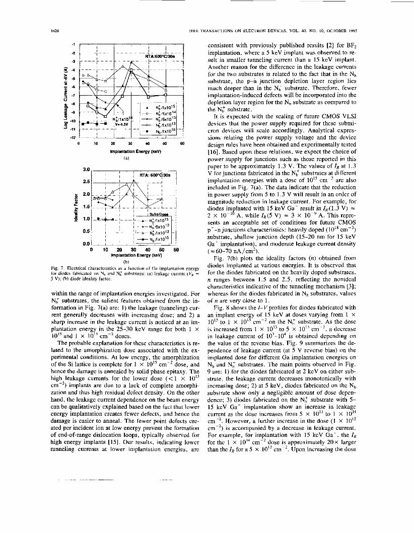
(b) Fig. 7 . Electrical characteristics as a function of Ga implantation energy for diodes fabricated on N, and NC substrates: (a) leakage current (VR = 5 V); (b) diode ideality factor.
within the range of implantation energies investigated. For Nb+ substrates, the salient features obtained from the in- formation in Fig. 7(a) are: 1) the leakage (tunneling) cur- rent generally decreases with increasing dose; and 2) a sharp increase in the leakage current is noticed at an im- plantation energy in the 25-30 keV range for both 1 x lOI5 and 1 X I O i 3 cmP2 doses.
The probable explanation for these characteristics is re- lated to the amorphization dose associated with the ex- perimental conditions. At low energy, the amorphization of the Si lattice is complete for 1 X 10" cmP2 dose, and hence the damage is annealed by solid phase epitaxy. The high leakage currents for the lower dose (< 1 X lOI5 cmP2) implants are due to a lack of complete amorphi- zation and thus high residual defect density. On the other hand, the leakage current dependence on the beam energy can be qualitatively explained based on the fact that lower energy implantation creates fewer defects, and hence the damage is easier to anneal. The fewer point defects cre- ated per incident ion at low energy prevent the formation of end-of-range dislocation loops, typically observed for high energy implants [ 151. Our results, indicating lower tunneling currents at lower implantation energies, are
consistent with previously published results [2] for BF2 implantation, where a 5 keV implant was observed to re- sult in smaller tunneling current than a 15 keV implant. Another reason for the difference in the leakage currents for the two substrates is related to the fact that in the Nb substrate, the p-n junction depletion layer region lies much deeper than in the Nbf substrate. Therefore, fewer implantation-induced defects will be incorporated into the depletion layer region for the N b substrate as compared to the NZ substrate.
It is expected with the scaling of future CMOS VLSI devices that the power supply required for these submi- cron devices will scale accordingly. Analytical expres- sions relating the power supply voltage and the device design rules have been obtained and experimentally tested [ 161. Based upon these relations, we expect the choice of power supply for junctions such as those reported in this paper to be approximately 1.3 V. The values of ZR at 1.3 V for junctions fabricated in the Nl substrates at different implantation energies with a dose of 10'' cmP2 are also included in Fig. 7(a). The data indicate that the reduction in power supply from 5 to 1.3 V will result in an order of magnitude reduction in leakage current. For example, for diodes implanted with 15 keV Ga' result in ZR (1.3 V) 1: 2 X IO-'' A, while ZR(5 V) = 3 x A. This repre- sents an acceptable set of conditions for future CMOS p' -n junctions characteristics: heavily doped ( 10l8 cmP3) substrate, shallow junction depth (15-20 nm for 15 keV Ga' implantation), and moderate leakage current density ( = 60-70 nA /cm2).
Fig. 7(b) plots the ideality factors (n) obtained from diodes implanted at various energies. It is observed that for the diodes fabricated on the heavily doped substrates, n ranges between 1.5 and 2.5, reflecting the nonideal characteristics indicative of the tunneling mechanism [3] ; whereas for the diodes fabricated in Nb substrates, values of n are very close to 1 .
Fig. 8 shows the I-Vprofiles for diodes fabricated with an implant energy of 15 keV at doses varying from 1 X l O I 3 to 1 x lOI5 cmP2 on the N: substrate. As the dose is increased from 1 x l O I 3 to 5 x IOI3 cm-2, a decrease in leakage current of 103-104 is obtained depending on the value of the reverse bias. Fig. 9 summarizes the de- pendence of leakage current (at 5 V reverse bias) on the implanted dose for different Ga implantation energies on Nb and N l substrates. The main points observed in Fig. 9 are: 1) for the diodes fabricated at 2 keV on either sub- strate, the leakage current decreases monotonically with increasing dose; 2) at 5 keV, diodes fabricated on the Nb substrate show only a negligible amount of dose depen- dence; 3) diodes fabricated on the Nbf substrate with 5- 15 keV Ga' implantation show an increase in leakage current as the dose increases from 5 x l O I 3 to 1 X 1014 cm-2. However, a further increase in the dose ( 1 X 10" cmP2) is accompanied by a decrease in leakage current. For example, for implantation with 15 keV Ga', the ZR for the 1 X lOI4 cmP2 dose is approximately 2 0 ~ larger than the In for a 5 x IOl3 cm-2. Upon increasing the dose

MOGUL et al.: ELECTRICAL PROPERTIES OF Si pi -n JUNCTIONS FOR SUB-0.25 pm CMOS
-2
-3 - -4 5 c -5 5 -6 0 Q -7
Y -8
c,
P 3 -9
3 -10
0
0
-1 1
E " " "" " " " " " ' . ' , - ' a
- 1 2 [ . . - " ~ ' " " " " "" , . , , ' I J
-5 -4 -3 -2 -1 0 1
Voltage (V)
Fig 8 Dose dependence of I-V characteristics of diodes fabricated on N l substrate
5keV A lOkeV
15keV
10 l3 10 l4 10 l3 10 l6
Implanted Dose (cm-* ) Fig. 9. Leakage current ( V R = 5 V) as a function of Ga implanted dose
for diodes fabricated on N, and NL substrates at different energies.
to 1 X 10" cm-2, it is observed that the IR decreases by 150X over the value obtained for 1 x IOl4 cm-2.
In order to study the effect of scan speed on the elec- trical characteristics, diodes were also fabricated with 5- 15 keV/ 1 X 1OIs cm-2 on an N l substrate using multiple scans (MS) by changing the dwell time of the implant. The net effect of multiple scans is to change the implan- tation dose rate. Using MS FIB implantation, defects are not generated continuously at any one location [ 171, and thus may have enough time to self-anneal to a certain ex- tent until the next scan. In the case of single-scan (SS) FIB implantation, each pixel receives the entire dose con- tinuously with a much-reduced opportunity to self-anneal, thus possibly leading to a higher final damage level. Fig. 10 compares the effect of multiple scans on the I-V char- acteristics. The data indicate that for reverse bias voltages greater than 5 V, there is no apparent scan speed depen- dence. At reverse bias < 5 V, a change in the leakage current is observed with respect to the scan speed. This could be due to the fact that at lower reverse bias, the depletion width region lies closer to the edge of the im- planted region. For most cases, it was observed that the leakage current of MS diodes is lower than that of SS
Voltage (V) -3
-4
-5 ?! 5 -6
-7 m
5 - 0 P)
Y
-8 J a 3 -9
-1 0
-3
4
-5
-6
-7
-0
-9
-1 0
-1 1
~
1827
-3 -1 2
-4
5
-7 a -8 9
-5 L
-6 ?!
al
-9 3 0)
4 -10
-11
-12
; " ' ' : I ' '
-10 -8 -6 -4 -2 0 2
Fig, 10. I -V characteristics of diodes fabricated on N l substrates using single scan and multiple scan Ga implantation at different energies.
diodes. Fig.10 also shows that as the implant energy in- creases from 5 to 15 keV, the forward characteristics of the N l diodes become insensitive to the effect of multiple scans. Multiple scan implantations on the Nb substrate re- sulted in diode I-V characteristics which showed only a very small scan speed dependence as compared to the N l samples. In general, it is interesting to note that while the number of implant scans are changed significantly, there is not an appreciable difference in the I-V charac- teristics of the FIB fabricated diodes.
I- V measurements were performed on diodes annealed at two different temperatures to observe the dependence of leakage current on anneal temperature. Fig. 11 com- pares the I-V characteristic of diodes fabricated on a N l substrate with 10 keV/ l X l O I 5 cm-* Ga implant and annealed at 600°C and at 700°C for 30 s . The figure shows that the diode annealed at 700°C is approximately IOOOX leakier than the diode annealed at 600°C. This effect can be attributed to a "reverse anneal," namely, a decrease in the electrical activity of the implanted ions when a certain critical anneal temperature is exceeded. This effect is consistent with the fact that Ga atoms im- planted into Si are known to precipitate easily and form

I828 IEEE TRANSACTIONS ON ELECTRON DEVICES, VOL. 40, NO. IO, OCTOBER 1993
-10 -8 -6 -4 -2 0 2
Voltage (V)
I-V charactenstics of diodes fabricated on NC substrates under Fig. 1 1 different RTA annealing conditions
10 -8
10-9
10 -10
Voltage (V)
-5 -4 -3 -2 -1 0 1 2 10 -11
Fig 12 C-V characteristics of diodes fabricated in N, and N t substrates
electrically inactive clusters when annealed at higher tem- peratures (exceeding 600°C) [ 181, [ 191. This behavior was also exhibited by diodes fabricated at 5 and 15 keV, with the leakage current at -5 V for diodes annealed at 600°C being 100-200X smaller than the corresponding diodes annealed at 700 O C.
Finally, Fig. 12 shows the capacitance-voltage (C-V) measurements made for diodes fabricated on the two dif- ferent substrates. As expected under reverse bias, the val- ues of capacitance for the lightly doped substrate are sig- nificantly lower than the corresponding values for the NZ substrate. The abrupt nature of these junctions was confirmed by plotting C2 versus V , which yielded a straight line as shown in the inset of Fig. 12.
IV. CONCLUSIONS A systematic study of energy and dose dependence of
FIB Ga’ implanted shallow junctions on Si substrates with a range of background concentrations has been per- formed. The results indicate that for N; substrates an op- timal implantation condition with regard to the electrical
properties exists at 15 keV/ l x lOI5 cm-’, while for Nb substrates, the I-I / characteristics were found to be rela- tively insensitive to implant energy. The tunneling com- ponent of the leakage current dominated the electrical properties of the diodes fabricated on the N l substrates. A major reason for the difference in the electrical prop- erties between diodes on the two different substrates could arise from the location of defects with respect to the diode depletion region. An RTA anneal of 6OO0C/30 s was de- termined to provide reduced leakage currents.
REFERENCES
[ I ] B. Park, J . Baker, H. Luftman, C. Rafferty, and M. Pinto, “Ultra- shallow junctions for ULSI using As implantation and rapid thermal anneal,” IEEE Electron Device Lett., vol. 13, p. 507, 1992.
[2] J . Stork and R. Isaac, “Tunneling in base-emitter junctions,” IEEE Trans. Electron Devices, vol. 30, p. 1527, 1983.
131 G . Hurkx, D. Klaassen. and M. Knuvers, “A new recombination model for device simulation including tunneling,” IEEE Trans. Elec- tron Devices, vol. 39, p. 331, 1992.
[4] J . Melngailis, “Focused ion beam technology and applications,” J . Vac. Sci. Technol., vol. B5, p. 469, 1987.
[5] A. J . Steckl, H. C. Mogul, and S. M. Mogren, “Ultrashallow Si p+- n junction fabrication by low energy Ga focused ion beam implanta- tion,” J . Vac. Sri. Technol., vol. B8, p. 1937, 1990.
161 A. J. Steckl, H. C. Mogul, S. W. Novak, and C. W. Magee, “Low energy off-axis focused ion beam Ga implantation into Si,” J . Vac. Sei. Technol., vol. B9, p. 2916, 1991.
[7] A . J . Steckl, H. C. Mogul, and S. Mogren, “Electrical properties of nanometer-scale Si pt-n junction fabricated by low energy Ga fo- cused ion beam implantation,” J . Vac. Sri. Technol., vol. B9, p. 2718, 1991.
[8] S. W . Novak, C. W. Magee, H. C. Mogul, and A. J . Steckl, “Sec- ondary ion mass spectrometry depth profiling of nanometer-scale p+- n junctions fabricated by Ga+ focused ion beam implantation,” J . Vac. Sei. Technol., vol. B10, p. 333, 1992.
[9] M. Tsai, B. Streetman, V. Deline, and C. Evans, “Gallium distri- bution and electrical activation in Ga implanted Si,” J . Elecrron. Mat., vol. 8, p. 111, 1979.
[IO] Y . Sasaki, K. Itoh, and T. M. Ituishi, “A new experimental deter- mination of relationship between Hall mobility and-the hole concen- tration in heavily doped p-type silicon,” Solid-State Electron., vol. 31, p. 5, 1988. H. C. Mogul, A. J . Steckl, G. Webster, M. Pawlik, and S. Novak, “Electrochemical capacitance-voltage depth profiling of nanometer- scale layers fabricated by Ga FIB implantation into Si,” Appl. Phys. Lett., vol. 61, p. 554, 1992. G. Li, E. Hackbarth, and T . Chen, “Identification and implication of a perimeter tunneling current component in advanced self-aligned bipolar transistor,” IEEE Trans. Electron Devices, vol. 35, p. 90, 1988. A . Cuthberston and P. Ashbum, “Self-aligned transistors with poly- silicon emitters for bipolar VLSI,” IEEE Trans. Electron Devices, vol. 32, p. 242, 1985. J . Lasky, “Rapid isothermal annealing of boron ion implanted junc- tions,” J . Appl. Phys., vol. 54, p. 6009, 1983. E. Ganin and A. Marwick, “Is the end-of-range loops kinetics af- fected by surface proximity or ion beam recoils distribution?” Mat. Res. Soc., vol. 147, p. 13, 1989. M. Kakumu, M. Kinugawa, K. Hashimoto, and J . Matsunaga, “Power supply voltage for future CMOS VLSI in half and sub mi- crometer,” in IEDM Tech. Dig., 1986. p. 399. H. Lezec, C . Musil, and J . Melngailis, “Dose-rate effects in focused ion beam implantation of Si into GaAs,” J . Vac. Sri. Technol., vol. B9, p. 2709, 1991. J. Matsuo, I. Kato, H . Horie, N. Nakayama, and H. Ishikawa, “Ab- normal solid solution and activation behavior in Ga-implanted Si(lOO),” Appl. Phys. Lett., vol. 51, p. 2037, 1987. H. C. Mogul, and A. J . Steckl, “Rapid thermal annealing effects on Si p+-n junctions fabricated by low-energy FIB Ga+ implantation,” IEEE Electron Device Lett., vol. 14, p. 123, 1993.

MOGUL et al.: ELECTRICAL PROPERTIES OF Si pt-n JUNCTIONS FOR SUB-0.25 Nm CMOS I829
Homyar C. Mogul is currently a Ph.D. student in the Department of Electrical Engineering at the University of Cincinnati working under the super- vision of Dr. Andrew J . Steckl. His research in- volves using Ga-based focused ion beam (FIB) implantation technology for application in fabri- cation of sub-quarter micron CMOS technology. His research interests include processing, fabri- cation and testing of sub-micron devices, silicide technology, characterization, sub-micron lithog- raphy, materials processing, flat-panel display de-
vices, Si-based optoelectronics technology, and exploratory structures/de- vices.
the University of Cincinnati as Ohio Eminent Scholar and Gieringer Pro- fessor of Solid State Microelectronics. At Cincinnati he has built the Nanoelectronics Laboratory whose mission is to investigate materials, fabrication techniques, and devices operating at the nanometer level. His research interests include focused ion beam fabrication of Si and compound semiconductor devices, S i c thin-film growth and device fabrication, photoluminescent porous Si and related devices, reactive ion etching, and atomic scale microscopy. His research has resulted in 160 publications and over 190 conference and seminar presentations.
Andrew J. Steckl (S’70-M’73-SM’79) received the B.S.E. degree in electrical engineering from Princeton University, Princeton, NJ, in 1968, and the M.Sc. and Ph.D. degrees from the University of Rochester, Rochester, NY, in 1970 and 1973, respectively.
In 1972, he joined the Honeywell Radiation Center, Lexington, MA, as a Senior Research En- gineer, where he worked on new concepts and de- vices in the area of infrared detection. In 1973, he joined the Technical Staff of the Electronics Re-
search Division of Rockwell Intemational, Anaheim, CA. At Rockwell he was primarily involved in research on charge coupled devices. In 1976, he joined the Electrical, Computer and Systems Engineering Department at Rensselaer Polytechnic Institute in Troy, NY, where he developed a re- search program in microfabrication of Si devices. In 1981, he initiated the Center for Integrated Electronics, a multi-disciplinary academic center fo- cused on VLSI research and teaching, and served as its director until 1986. In 1988, he joined the Electrical and Computer Engineering Department of
Eti Ganin graduated from the Leningrad Poly- technical Institute, Faculty of Physics and Me- chanics, St. Petersburg, former USSR. She re- ceived the M.S. and D.Sc. degrees from the Technion-Israel Institute of Technology in Haifa, Materials Engineering Department. Her D.Sc. dissertation, completed in 1984, concerned the nature of bonding between explosively welded copper and its alloys.
She joined IBM, T. J. Watson Research Center as a post-doctoral fellow in 1985, where she was
involved with processing ultrasmall device structures. Her research inter- ests include ultra-shallow junctions for silicon devices, silicide reactions and characterization in VLSI processing. She is also interested in ion im- plantation damage and dopant interaction related to shallow junction for- mation. She is currently working as an Advisory engineer in Advanced Logic and SRAM Group, IBM, East Fishkill Facility, New York.
Dr. Ganin is a member of the American Physical Society and the Ma- terials Research Society.


![Performance of the ATLAS Tile Calorimeter · 2019. 12. 1. · To maximise the use of radial space, the girder provides both ... cated [113]. The master plate was fabricated by high-precision](https://static.fdocument.org/doc/165x107/5fdef10c222d6925e63cf3ce/performance-of-the-atlas-tile-calorimeter-2019-12-1-to-maximise-the-use-of.jpg)