High Dose Irradiation of Possible FCAL Sensors at the S-DALINAC
1
Effect of E-Beams Irradiation Dose on the Sensing
Properties of Pt-Functionalized Reduced Graphene
Oxides Following Annealing of the 6 nm-Thick Pt Layer
Yong Jung Kwon1, Ali Mirzaei
2, Han Gil Na
1, Sung Yong Kang
1, Myung Sik Choi
1, Jae
Hoon Bang1, Jaegab Lee
3, Inpil Kang
4, Sang Sub Kim
5,*,and Hyoun Woo Kim
1,2**
1Division of Materials Science and Engineering, Hanyang University, Seoul 04763, Republic
of Korea
2The Research Institute of Industrial Science, Hanyang University, Seoul 04763, Republic of
Korea
3School of Advanced Materials Engineering, Kookmin University, Seoul 02707, Republic of
Korea
4Department of Mechanical Design Engineering, Pukyong National University, Busan 48547,
Republic of Korea
5Department of Materials Science and Engineering, Inha University, Incheon 22212,
Republic of Korea
Pt-functionalized RGO samples were prepared and subsequently irradiated with 2-MeV
electron beams (e-beams). The effect of e-beam dose on the structural, electrical, and gas
sensing properties of the samples was investigated. E-beam irradiation was found to induce
significant microstructural changes in the Pt-functionalized RGO. Measurements of NO2
sensing at room temperature showed that the dose of 100 kGy led to better NO2 sensing
properties compared to those of unirradiated sensors. On the other hand, the dose of 500 kGy
appeared to be excessive, leading to extensive damage of the RGO structure and a significant
reduction in the response to NO2 gas. E-beam irradiation can be beneficial for improving the
gas sensing of Pt-functionalized RGO, but its dose needs to be optimized to obtain the best
sensing properties.
2
Keywords: reduced graphene oxide, gas Sensor, E-Beam Irradiation, Pt nanoparticles,
NO2.
(Received November 1, 2016; Accepted December 19, 2016)
* Corresponding author at: Tel: +82 32 960 7546; fax: +82 32 862 5546; E-mail address:
[email protected] (S.S. Kim.)
** Corresponding author at: Tel: +82 2 2220 0382; fax: +82 2 2220 0389; E-mail address:
[email protected] (H.W. Kim).
1. INTRODUCTION
The nano era has been, a tremendous increase in the number of reports discussing methods
of fabricating and characterizing a variety of nanomaterials and nanostructures [1-20].
Among these, a new generation of gas sensors based on graphene materials such as graphene
oxide, and reduced graphene oxide (RGO) have drawn attention, due to their room
temperature operation, facile synthesis, and the ease with which their electrical properties can
be tailored [21]. RGO-based gas sensors based on noble metal nanoparticles (NPs), used as
either composite materials or decorating particles, have demonstrated better sensing
properties than pristine RGO sensors [22,23]. This performance enhancement is due to the
increase in electronic and chemical sensitivity provided by the noble metals. The electronic
sensitization originates from the flow of electrons between the sensing material and the metal
NPs. The chemical sensitization is due to the catalytic effect of the metal NPs; the metal NPs
can facilitates either the adsorption of target gases or their efficient transport to the sensing
material. Furthermore, they induce increased interactions with preadsorbed oxygen species,
facilitating the relevant chemical reactions [24]. However, for advanced applications, the
sensing properties of RGO-based chemiresistive sensors still need further enhancement.
To enhance the sensing properties of gas sensors, a number of post-treatment modifications
have been explored, including exposure to highly energetic radiation such as e-beams [25],
ion beams [26], and gamma rays [27]. Different types of irradiation can produce significant
microstructural and morphological changes in various materials such as polymers, ceramics,
and semiconductors. More specifically, they can create a wide variety of defects in the
materials, which ultimately modify their optical, electrical, and sensing properties [28]. For
example, gamma radiation has been observed to decrease the electron mobility of n-GaN by
introducing defects that act as scattering centers [29]. Yin et al. reported that indium vanadate
nanoribbons irradiated with gamma rays showed enhanced ammonia sensing, which was
3
attributed to the creation of defects [30]. Bal et al. reported that ion bombardment of a ZnO
nanowire-based sensor decreased its response to ammonia gas and increased its recovery
speed. They attributed these results to the rupturing of the nanostructure under irradiation,
which decreased porosity and hindered the diffusion of gas molecules into the inner part of
the sample [31]. Kwon et al. attributed improvement in the gas sensing properties of pristine
RGO after e-beam irradiation to the formation of defects [32].
Among the various irradiation methods, e-beams have recently been extensively studied as a
means of preparing noble metal NPs [33], bimetallic NPs [34], and core–shell NPs [35], and
have also been used to controllably introduce defects in order to modify materials’ optical
and electrical properties [36].
E-beams lose their energy when passing through materials due to interactions with atoms.
At lower energies, elastic collisions of e-beams and atoms are the dominant form of loss,
whereas at higher energies inelastic collisions between the energetic ions and atoms are
dominant [26]. High-dose irradiation of materials leads to the formation of lattice defects
such as vacancies, defect clusters, and dislocations. These defects can act as recombination
centers by trapping generated carriers. In addition, exposure to high levels of radiation leads
to significant changes in the electrical characteristics of metal oxides. In particular, there are
two important effects of e-beam radiation: these are transient effects due to electron–hole pair
generation and permanent effects which change the crystal lattice of the material [37].
In the present study we used e-beams with 2 MeV energy, applied at two different doses,
100 and 500 kGy. This level of high-energy e-beams can ionize RGO. Upon ionization, the
generated ions capture negatively charged electrons or positively charged holes, creating
defects. These defects cause changes in the microstructure and in the distribution of oxygen
vacancies in the material. Radiation can also lead to the segregation and diffusion of atoms,
leading to phase segregation and voids. Accordingly, e-beam radiation can be used to modify
the physical and chemical properties of the irradiated material [37].
Although there have been numerous reports regarding the gas sensing properties of noble
metal/RGO materials [38-40], to the best knowledge of the authors, there have been very few
reports regarding the effect of e-beam irradiation on the sensing behavior of RGO-based
sensors. Accordingly, the present work studies the effect of e-beam dose on the NO2 sensing
behavior of Pt-functionalized RGO sensors. The RGO used was prepared by the chemical
reduction of GO, and sensors were prepared by sputtering 6 nm thick Pt layers onto RGO,
followed by thermal annealing. The effect of e-beam dose upon the structure of the RGO was
4
investigated. Also, the NO2 sensing properties of various sensors were studied and compared,
including sensors based on either pristine RGO or Pt-functionalized RGO, and between RGO
those subjected to no irradiation or to irradiation at various doses.
2. EXPERIMENTAL PROCEDURES
2.1 SYNTHESIS AND E-BEAM IRRADIATION
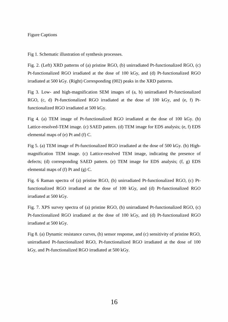
Figure 1 schematically illustrates the RGO synthesis procedure. Hummers’ method was
employed to convert graphite into GO [41]; more details are given in our previous paper [42].
The graphite oxidation process was started by stirring graphite (1 g) in an oxidizing mixture
of concentrated H2SO4 (46 ml) containing KMnO4 (12 g) and H3PO4 (12 g). This procedure
increases the interlayer distance between the packed graphite layers, thereby facilitating
exfoliation and separation of graphene sheets. A very fine brown powder was obtained after
repeated washing and filtration; this was dried in a vacuum oven. The powder was mixed
with hydrazine monohydrate and heated at 150 °C in an oil bath, yielding RGO. To prepare a
homogenous suspension of RGO, it was dispersed in dimethylformamide (C3H7NO) and
subsequently sonicated. The RGO suspension was coated onto quartz substrates, and then
heated at 250 °C for 3 h to dry it. Annealing of the resulting RGO films was performed at
1100 °C for 30 min under a 100 sccm flow of mixed Ar and H2 gas.
A turbo sputter coater with a circular Pt target (Emitech K575X, Emitech Ltd., Ashford,
Kent, UK) was used to perform room-temperature coating of the Pt. To prepare Pt layers of
6nm thickness on the RGO samples, plasma sputtering was conducted in the presence of Ar
gas, using the controlled deposition time of 10 s and the DC sputter current of 65 mA. Finally,
to convert each Pt layer into a layer of Pt with NPs dispersed over the surface of the RGO, it
was annealed at 700 °C for 0.5 h under a 2000 sccm flow of Ar gas.
Irradiation of the Pt-functionalized RGO films was performed in air atmosphere at room
temperature. E-beam irradiation was conducted at the ELV-8 electron accelerator (EBTech,
Daejeon, Korea). The accelerating energy of 2 MeV was used with the two different doses of
100 and 500 kGy to study the effect of dose on the resulting films’ physical properties and
sensing behavior. The beam current was set at 1 mA and the pulse duration was fixed at 400
ps.
2.2. MATERIAL CHARACTERIZATION
5
To study the structure and phase formation of the prepared samples, X-ray diffraction (XRD)
patterns were acquired under Cu Kα (λ = 1.541 Å) radiation (Rigaku, Japan). To examine the
morphological features of the Pt-functionalized RGO samples, we conducted scanning
electron microscopy (SEM; JSM 5900 LV, JEOL, Japan), as well as transmission electron
microscopy (HR-TEM; TECNAI 20, FEI, USA; with an accelerating voltage of 200 kV)
coupled with energy dispersive spectrometry (EDS). Raman scattering under an Ar-ion laser
source (532 nm, 2.33 eV) was measured in air at RT using a Horiba Jobin-Yvon LabRam HR
Evolution system, equipped with a confocal microscope (100× microscope objective lens). A
low laser power density of 265 μW at the sample surface was used to prevent laser-induced
annealing effects. To analyze elemental compositions, X-ray photoelectron spectroscopy
(XPS; VG Multilab ESCA 2000 system, UK) was conducted using a monochromatized Al Kα
X-ray source (hν = 1486.6 eV) at the Korean Basic Science Institute. The binding energies
obtained from the XPS analysis were corrected for specimen charging by calibrating the C1s
line to 284.5 eV.
2.3 GAS SENSING MEASUREMENTS
To enable gas sensing studies, double-layer electrodes of Ni (~200 nm thickness) and Au
(~50 nm thickness) were sputtered onto sample films using an interdigitated electrode mask.
The sensing setup used was similar to that previously described by our research group [43].
To test each sample’s sensing properties, it was placed in a tubular furnace that was
electrically connected to a measuring system (Keithley 2400) interfaced with a computer. The
NO2 concentration (10 ppm) was precisely controlled by changing the mixing ratio of the
NO2 and dry air using mass flow controllers, maintaining the total flow rate of 100 sccm.
Resistances were measured in the presence of air (Ra) and NO2 (Rg) at room temperature; the
sensor response was defined as R = Ra/Rg. The response time was defined as the time
required for the change in electrical resistance to reach 90% of the equilibrium value after the
injection of NO2 gas, and the recovery time was defined as the time needed for the sensor to
return to 90% of its initial resistance in air after removing the supply of NO2.
3. RESULTS AND DISCUSSION
3.1 STRUCTURAL, MORPHOLOGICAL, AND CHEMICAL ANALYSES
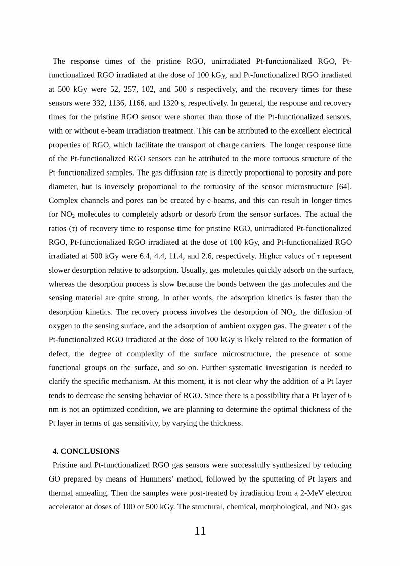
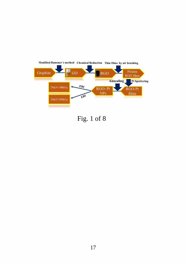
Figures 2a–d show XRD patterns of the various sensors. Figure 2a shows an XRD spectrum
of pristine RGO, in which only two carbon peaks were observed, namely the (002) and (101)
6
peaks. On the other hand, one additional peak was observed in each of the spectra of the Pt-
functionalized RGO samples (Figs. 2b–d), ignoring the Si peaks originating from the
substrate, which belonged to the {111} plane of Pt. This peak confirms the formation of
crystalline Pt in the samples. Magnified XRD spectra focusing on the (002) carbon peak are
shown in the left part of Fig. 2. For the pristine RGO samples, samples of Pt-functionalized
RGO with no irradiation, Pt-functionalized RGO irradiated at the dose of 100 kGy, and Pt-
functionalized RGO irradiated at 500 kGy, the peak positions of the (002) plane were
respectively located at 24.43°, 26.29°, 26.32°, and 26.45°. This means the peak positions
were shifted to higher Bragg diffraction angles with increasing dose, which corresponds to a
slight decrease in the lattice spacing. Possible reasons for this small decrease in lattice
spacing include the presence of residual compression strains caused by either the sputtering
process or the electron. E-beam irradiation can cause lattice strain because it can introduce of
oxygen vacancies and surface defects [44].
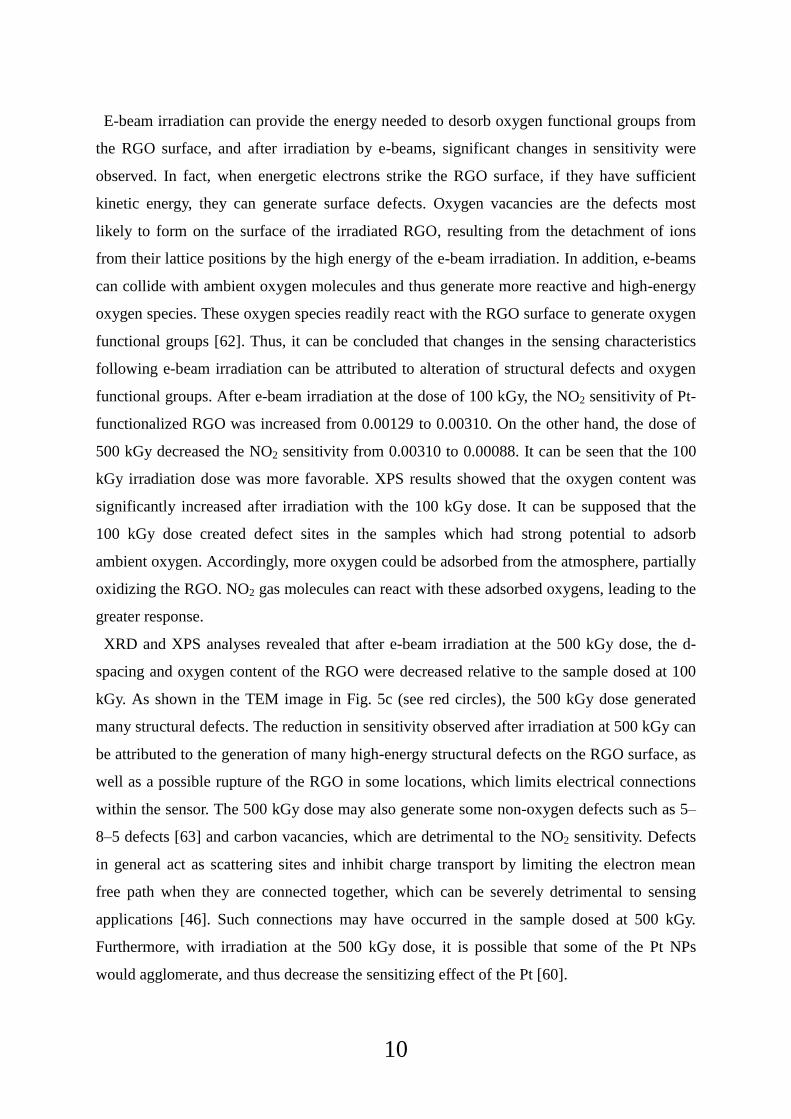
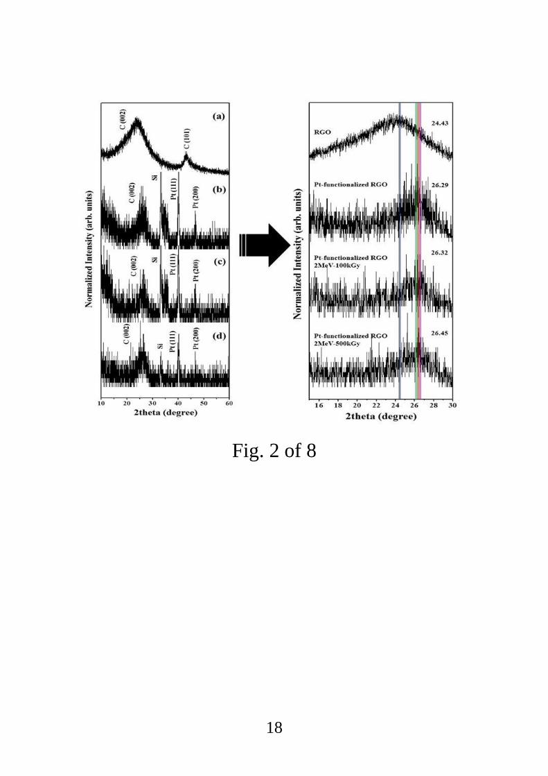
SEM micrographs of each Pt-functionalized RGO sample clearly showed fine and dispersed
Pt NPs in a matrix of carbon (Fig. 3). The unirradiated sample had a relatively smooth surface
while the sample dosed at 100 kGy had a slightly rougher surface. The sample that received
the high e-beam dose of 500 kGy showed a rougher and more complicated surface. However,
the SEM images did not allow a more detailed evaluation of the effects of the e-beam
irradiation on the final morphology. For that, further analysis using TEM was conducted.
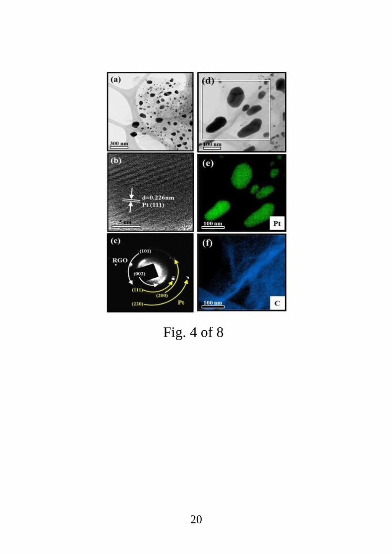
In the TEM image of Pt-functionalized RGO irradiated at 100 kGy in fig. 4a, RGO sheets
functionalized with Pt NPs (5–50 nm) can be easily seen. A HRTEM image showed that the
spacing between the two lattice fringes was about 0.226 nm (Fig. 4b), which can be attributed
to the (111) plane of Pt having a fcc crystal structure. In a selected area electron diffraction
(SAED) pattern of this sample, ring patterns of the (101) and (002) planes of RGO and the
(111), (200), and (220) planes of Pt confirmed the presence of both Pt and RGO in the sample
(Fig. 4c). Elemental mapping analysis further verified the presence of fine and dispersed Pt
NPs in a matrix of carbon (Figs. 4d–f). Similarly, in low-magnification TEM and HRTEM
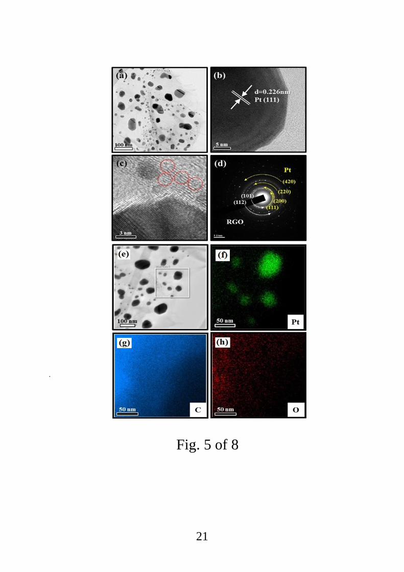
images of the sample irradiated with 500 kGy the existence of Pt NPs in a carbon matrix was
evident (Fig. 5a, b). A lattice-resolved image of this sample shows multiple defects generated
by the high-energy e-beams (Fig. 5c; see red circles). In fact, if the kinetic energy transferred
to the RGO is greater than a threshold value for bond breaking, the carbon atoms will be
displaced on a sub-picosecond time scale, generating vacancies at their prior sites [45]. In the
SAED pattern in Fig. 5d, rings corresponding to the (111), (200), (220), and (420) planes of
7
polycrystalline Pt and the (101) and (112) planes of polycrystalline carbon can be clearly
seen . In EDS elemental maps of the TEM image in Figs. 5e-h, some traces of oxygen are
observed; this most likely is due to the inclusion of atmospheric oxygen, adsorbed at the
many defect sites created by the e-beam irradiation, as well as the oxygen functional groups
of the RGO.
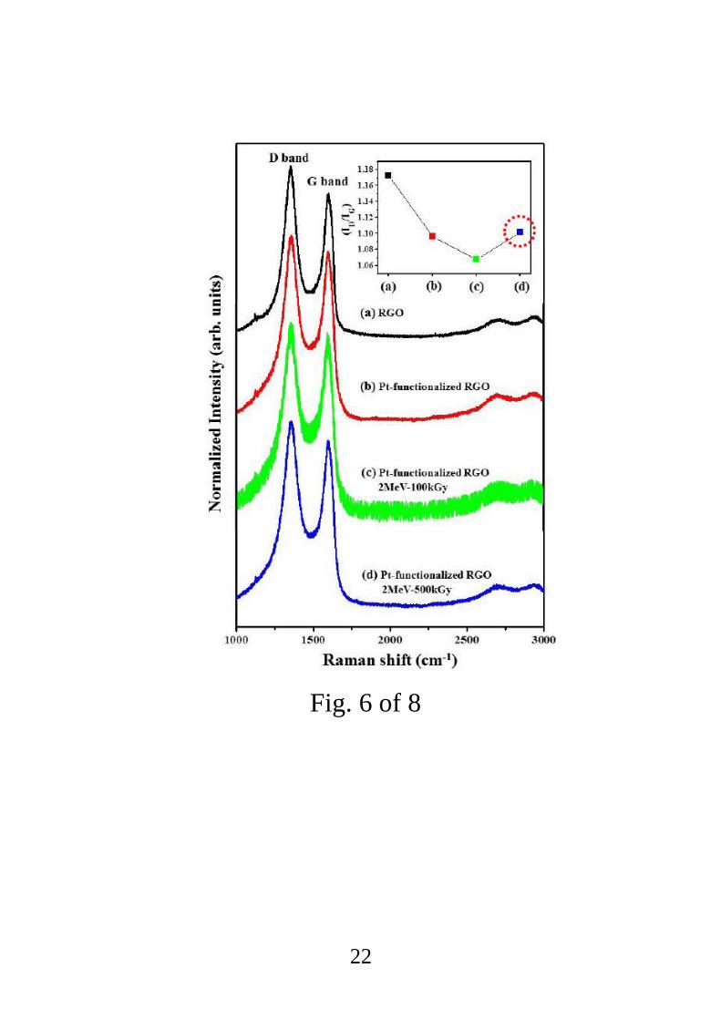
Raman spectra of the pristine and Pt-functionalized RGOs showed fingerprints of various
carbon allotropes, mostly in the D and G peak regions around 1350 and 1580 cm−1
,
respectively, caused by changes in the electron bands. Identification of these features allows
the graphene to be characterized in several ways, including the number of layers present, the
effects of strain, doping concentration and temperature, and the presence of defects [46]. The
main Raman band in graphene, known as the G band (~1580 cm−1
), corresponds to the E2g
mode. The line shape of the G band varies based on the sample quality, but this band exists
for all sp2 carbon systems, including amorphous carbon, carbon nanotubes, and graphite [47].
The D band, which is disorder-induced and occurs at around 1350 cm−1
is another important
band. Unlike the G band, to be present the D band requires defects for momentum
conservation [47]. The empirical Tuinstra–Koenig relation [48], which is the ratio of the
intensity of the D and G peaks (ID/IG), represents the degree of order across the graphitic
planes and defect levels. Smaller values of this ratio represent greater regularity, and greater
ratios indicate more defects and disorder [49]. The ID/IG values of pristine RGO, Pt-
functionalized RGO, Pt-functionalized RGO irradiated at the dose of 100 kGy, and Pt-
functionalized RGO irradiated at 500 kGy were estimated from Raman spectra to be 1.17,
1.09, 1.07, and 1.10, respectively. Although providing the exact mechanism for the variations
in ID/IG is beyond the scope of this work, we suggest the following qualitative explanation. It
is supposed that during the reduction process, many defects are generated in the carbon 2D
lattice (including point defects or the incomplete removals of epoxy/oxygenated functional
groups) [46]. However, after Pt functionalization, due to the reduction in the RGO surface
area, the number of defects is also reduced. Then, during e-beam irradiation, the removal of
oxygen functional groups is accompanied by the creation of more defects. However at the
same time, the RGO is oxidized, which decreases the numbers of defects. In other words,
defects were created after irradiation at the 100 kGy dose due to the creation of oxygen
vacancies, but oxygen species were also adsorbed from ambient air onto the active defects of
RGO, thereby decreasing the number of active defects. After irradiation at the dose of 500
8
kGy, however, there were many more defects, so even after oxidation some active defects
remain [50].
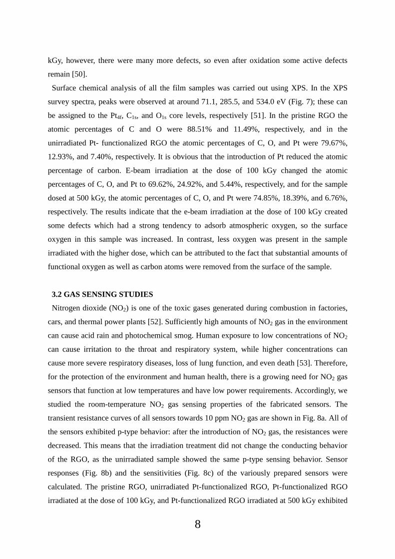
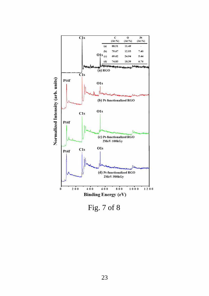
Surface chemical analysis of all the film samples was carried out using XPS. In the XPS
survey spectra, peaks were observed at around 71.1, 285.5, and 534.0 eV (Fig. 7); these can
be assigned to the Pt4f, C1s, and O1s core levels, respectively [51]. In the pristine RGO the
atomic percentages of C and O were 88.51% and 11.49%, respectively, and in the
unirradiated Pt- functionalized RGO the atomic percentages of C, O, and Pt were 79.67%,
12.93%, and 7.40%, respectively. It is obvious that the introduction of Pt reduced the atomic
percentage of carbon. E-beam irradiation at the dose of 100 kGy changed the atomic
percentages of C, O, and Pt to 69.62%, 24.92%, and 5.44%, respectively, and for the sample
dosed at 500 kGy, the atomic percentages of C, O, and Pt were 74.85%, 18.39%, and 6.76%,
respectively. The results indicate that the e-beam irradiation at the dose of 100 kGy created
some defects which had a strong tendency to adsorb atmospheric oxygen, so the surface
oxygen in this sample was increased. In contrast, less oxygen was present in the sample
irradiated with the higher dose, which can be attributed to the fact that substantial amounts of
functional oxygen as well as carbon atoms were removed from the surface of the sample.
3.2 GAS SENSING STUDIES
Nitrogen dioxide (NO2) is one of the toxic gases generated during combustion in factories,
cars, and thermal power plants [52]. Sufficiently high amounts of NO2 gas in the environment
can cause acid rain and photochemical smog. Human exposure to low concentrations of NO2
can cause irritation to the throat and respiratory system, while higher concentrations can
cause more severe respiratory diseases, loss of lung function, and even death [53]. Therefore,
for the protection of the environment and human health, there is a growing need for NO2 gas
sensors that function at low temperatures and have low power requirements. Accordingly, we
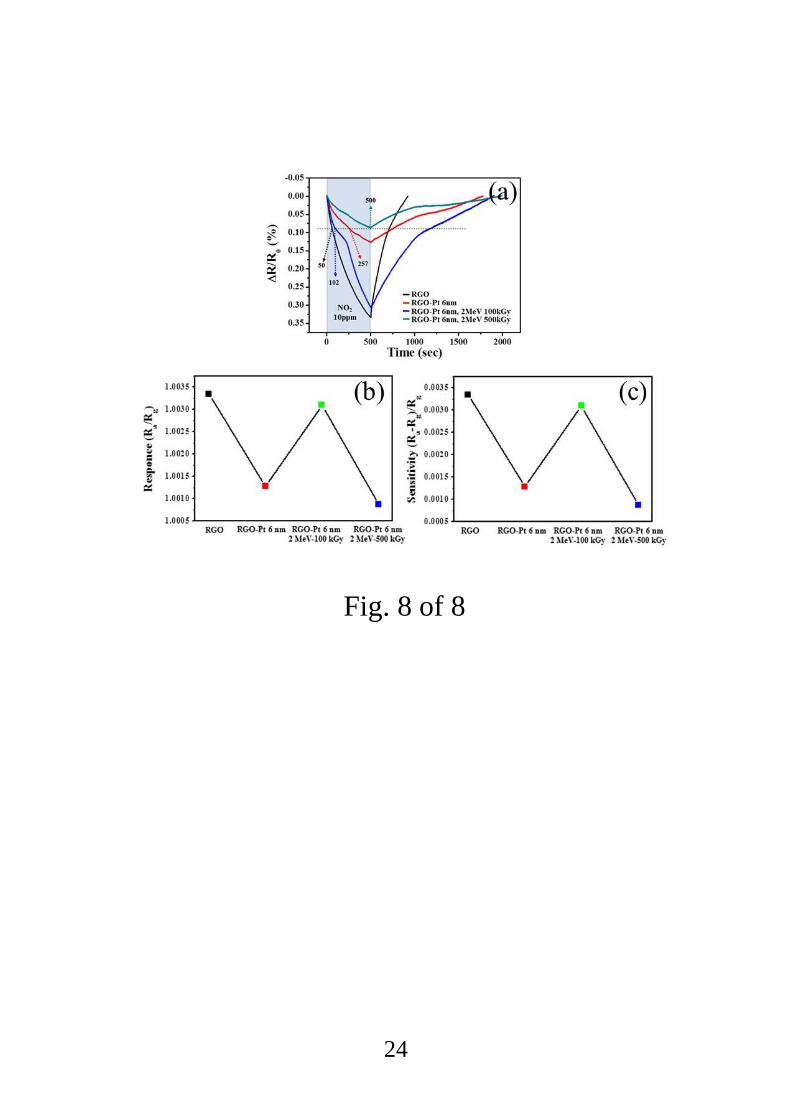
studied the room-temperature NO2 gas sensing properties of the fabricated sensors. The
transient resistance curves of all sensors towards 10 ppm NO2 gas are shown in Fig. 8a. All of
the sensors exhibited p-type behavior: after the introduction of NO2 gas, the resistances were
decreased. This means that the irradiation treatment did not change the conducting behavior
of the RGO, as the unirradiated sample showed the same p-type sensing behavior. Sensor
responses (Fig. 8b) and the sensitivities (Fig. 8c) of the variously prepared sensors were
calculated. The pristine RGO, unirradiated Pt-functionalized RGO, Pt-functionalized RGO
irradiated at the dose of 100 kGy, and Pt-functionalized RGO irradiated at 500 kGy exhibited
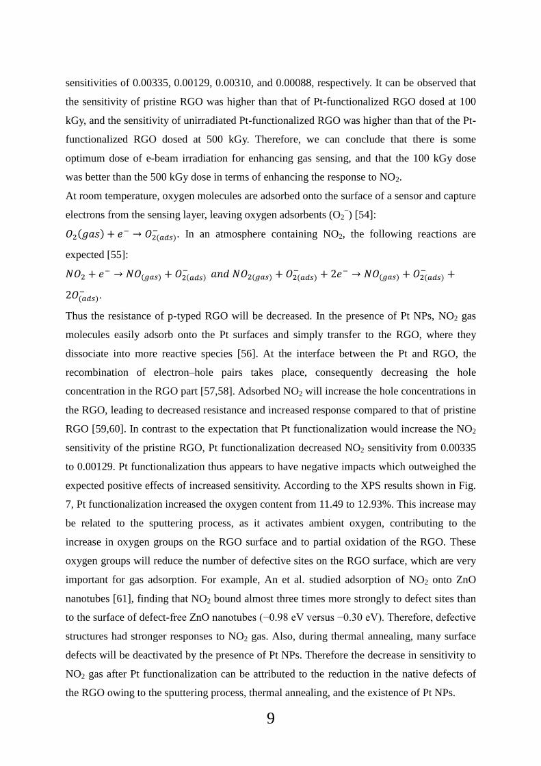
9
sensitivities of 0.00335, 0.00129, 0.00310, and 0.00088, respectively. It can be observed that
the sensitivity of pristine RGO was higher than that of Pt-functionalized RGO dosed at 100
kGy, and the sensitivity of unirradiated Pt-functionalized RGO was higher than that of the Pt-
functionalized RGO dosed at 500 kGy. Therefore, we can conclude that there is some
optimum dose of e-beam irradiation for enhancing gas sensing, and that the 100 kGy dose
was better than the 500 kGy dose in terms of enhancing the response to NO2.
At room temperature, oxygen molecules are adsorbed onto the surface of a sensor and capture
electrons from the sensing layer, leaving oxygen adsorbents (O2−) [54]:
𝑂2(𝑔𝑎𝑠) + 𝑒− → 𝑂2(𝑎𝑑𝑠)− . In an atmosphere containing NO2, the following reactions are
expected [55]:
𝑁𝑂2 + 𝑒− → 𝑁𝑂(𝑔𝑎𝑠) + 𝑂2(𝑎𝑑𝑠) − 𝑎𝑛𝑑 𝑁𝑂2(𝑔𝑎𝑠) + 𝑂2(𝑎𝑑𝑠)
− + 2𝑒− → 𝑁𝑂(𝑔𝑎𝑠) + 𝑂2(𝑎𝑑𝑠)− +
2𝑂(𝑎𝑑𝑠)− .
Thus the resistance of p-typed RGO will be decreased. In the presence of Pt NPs, NO2 gas
molecules easily adsorb onto the Pt surfaces and simply transfer to the RGO, where they
dissociate into more reactive species [56]. At the interface between the Pt and RGO, the
recombination of electron–hole pairs takes place, consequently decreasing the hole
concentration in the RGO part [57,58]. Adsorbed NO2 will increase the hole concentrations in
the RGO, leading to decreased resistance and increased response compared to that of pristine
RGO [59,60]. In contrast to the expectation that Pt functionalization would increase the NO2
sensitivity of the pristine RGO, Pt functionalization decreased NO2 sensitivity from 0.00335
to 0.00129. Pt functionalization thus appears to have negative impacts which outweighed the
expected positive effects of increased sensitivity. According to the XPS results shown in Fig.
7, Pt functionalization increased the oxygen content from 11.49 to 12.93%. This increase may
be related to the sputtering process, as it activates ambient oxygen, contributing to the
increase in oxygen groups on the RGO surface and to partial oxidation of the RGO. These
oxygen groups will reduce the number of defective sites on the RGO surface, which are very
important for gas adsorption. For example, An et al. studied adsorption of NO2 onto ZnO
nanotubes [61], finding that NO2 bound almost three times more strongly to defect sites than
to the surface of defect-free ZnO nanotubes (−0.98 eV versus −0.30 eV). Therefore, defective
structures had stronger responses to NO2 gas. Also, during thermal annealing, many surface
defects will be deactivated by the presence of Pt NPs. Therefore the decrease in sensitivity to
NO2 gas after Pt functionalization can be attributed to the reduction in the native defects of
the RGO owing to the sputtering process, thermal annealing, and the existence of Pt NPs.
10
E-beam irradiation can provide the energy needed to desorb oxygen functional groups from
the RGO surface, and after irradiation by e-beams, significant changes in sensitivity were
observed. In fact, when energetic electrons strike the RGO surface, if they have sufficient
kinetic energy, they can generate surface defects. Oxygen vacancies are the defects most
likely to form on the surface of the irradiated RGO, resulting from the detachment of ions
from their lattice positions by the high energy of the e-beam irradiation. In addition, e-beams
can collide with ambient oxygen molecules and thus generate more reactive and high-energy
oxygen species. These oxygen species readily react with the RGO surface to generate oxygen
functional groups [62]. Thus, it can be concluded that changes in the sensing characteristics
following e-beam irradiation can be attributed to alteration of structural defects and oxygen
functional groups. After e-beam irradiation at the dose of 100 kGy, the NO2 sensitivity of Pt-
functionalized RGO was increased from 0.00129 to 0.00310. On the other hand, the dose of
500 kGy decreased the NO2 sensitivity from 0.00310 to 0.00088. It can be seen that the 100
kGy irradiation dose was more favorable. XPS results showed that the oxygen content was
significantly increased after irradiation with the 100 kGy dose. It can be supposed that the
100 kGy dose created defect sites in the samples which had strong potential to adsorb
ambient oxygen. Accordingly, more oxygen could be adsorbed from the atmosphere, partially
oxidizing the RGO. NO2 gas molecules can react with these adsorbed oxygens, leading to the
greater response.
XRD and XPS analyses revealed that after e-beam irradiation at the 500 kGy dose, the d-
spacing and oxygen content of the RGO were decreased relative to the sample dosed at 100
kGy. As shown in the TEM image in Fig. 5c (see red circles), the 500 kGy dose generated
many structural defects. The reduction in sensitivity observed after irradiation at 500 kGy can
be attributed to the generation of many high-energy structural defects on the RGO surface, as
well as a possible rupture of the RGO in some locations, which limits electrical connections
within the sensor. The 500 kGy dose may also generate some non-oxygen defects such as 5–
8–5 defects [63] and carbon vacancies, which are detrimental to the NO2 sensitivity. Defects
in general act as scattering sites and inhibit charge transport by limiting the electron mean
free path when they are connected together, which can be severely detrimental to sensing
applications [46]. Such connections may have occurred in the sample dosed at 500 kGy.
Furthermore, with irradiation at the 500 kGy dose, it is possible that some of the Pt NPs
would agglomerate, and thus decrease the sensitizing effect of the Pt [60].
11
The response times of the pristine RGO, unirradiated Pt-functionalized RGO, Pt-
functionalized RGO irradiated at the dose of 100 kGy, and Pt-functionalized RGO irradiated
at 500 kGy were 52, 257, 102, and 500 s respectively, and the recovery times for these
sensors were 332, 1136, 1166, and 1320 s, respectively. In general, the response and recovery
times for the pristine RGO sensor were shorter than those of the Pt-functionalized sensors,
with or without e-beam irradiation treatment. This can be attributed to the excellent electrical
properties of RGO, which facilitate the transport of charge carriers. The longer response time
of the Pt-functionalized RGO sensors can be attributed to the more tortuous structure of the
Pt-functionalized samples. The gas diffusion rate is directly proportional to porosity and pore
diameter, but is inversely proportional to the tortuosity of the sensor microstructure [64].
Complex channels and pores can be created by e-beams, and this can result in longer times
for NO2 molecules to completely adsorb or desorb from the sensor surfaces. The actual the
ratios (τ) of recovery time to response time for pristine RGO, unirradiated Pt-functionalized
RGO, Pt-functionalized RGO irradiated at the dose of 100 kGy, and Pt-functionalized RGO
irradiated at 500 kGy were 6.4, 4.4, 11.4, and 2.6, respectively. Higher values of τ represent
slower desorption relative to adsorption. Usually, gas molecules quickly adsorb on the surface,
whereas the desorption process is slow because the bonds between the gas molecules and the
sensing material are quite strong. In other words, the adsorption kinetics is faster than the
desorption kinetics. The recovery process involves the desorption of NO2, the diffusion of
oxygen to the sensing surface, and the adsorption of ambient oxygen gas. The greater τ of the
Pt-functionalized RGO irradiated at the dose of 100 kGy is likely related to the formation of
defect, the degree of complexity of the surface microstructure, the presence of some
functional groups on the surface, and so on. Further systematic investigation is needed to
clarify the specific mechanism. At this moment, it is not clear why the addition of a Pt layer
tends to decrease the sensing behavior of RGO. Since there is a possibility that a Pt layer of 6
nm is not an optimized condition, we are planning to determine the optimal thickness of the
Pt layer in terms of gas sensitivity, by varying the thickness.
4. CONCLUSIONS
Pristine and Pt-functionalized RGO gas sensors were successfully synthesized by reducing
GO prepared by means of Hummers’ method, followed by the sputtering of Pt layers and
thermal annealing. Then the samples were post-treated by irradiation from a 2-MeV electron
accelerator at doses of 100 or 500 kGy. The structural, chemical, morphological, and NO2 gas
12
sensing properties of the synthesized samples were studied in detail using different
techniques. TEM and EDS analyses showed the presence of dispersed Pt NPs on the surfaces
of the RGO layers. NO2 gas sensing measurements at room temperature showed that after e-
beam irradiation at a dose of 100 kGy, the response was increased relative to that of an
unirradiated Pt-functionalized sample. This improved performance was attributed to the
presence of an optimum amount of defects and functional oxygen groups in the sample. In
contrast, when samples were irradiated with a dose of 500 kGy, the response was decreased,
possibly owing to the formation of a large network of connected defect sites. These results
demonstrated the beneficial effect of e-beam irradiation for improving the gas sensing
response of Pt-functionalized RGO.
ACKNOWLEDGEMENTS
This research was supported by Basic Science Research Program through the National Research
Foundation of Korea (NRF) funded by the Ministry of Education (2016R1A6A1A03013422). This
work was supported by the National Research Foundation of Korea (NRF) Grant funded by the
Korean Government (MSIP) (No. Grant Number - 2015R1A5A7037615).
13
REFERENCES
1. K. Bhowmik and A. Mondal, Electron. Mater. Lett. 11, 180 (2015).
2. D. N. Andoshe, J. -M. Jeon, S. Y. Kim, and H. W. Jang, Electron. Mater. Lett. 11, 180 (2015).
3. S. P. Khatkar, S. Singh, S. Lohra, A. Khatkar, and V. Taxak, Electron. Mater. Lett. 11, 409
(2015).
4. T. -J. Ha and A. Lee, Electron. Mater. Lett. 11, 552 (2015).
5. M. O. Ansari, M. M. Khan, S. A. Ansari, and M. H. Cho, Electron. Mater. Lett. 11, 559
(2015).
6. G. Anoop, E. Y. Park, S. Lee, and G. Y. Jo, Electron. Mater. Lett. 11, 565 (2015).
7. S. Park, G. -J. Sun, S. Kim, S. Lee, and C. Lee, Electron. Mater. Lett. 11, 572 (2015).
8. P. Kondaiah, H. Shaik, and G. M. Rao, Electron. Mater. Lett. 11, 592 (2015).
9. M. Karimipour, S. Mashhoun, M. Mollaei, M. Molaei, and N. Taghavinia, Electron. Mater.
Lett. 11, 625 (2015).
10. D. Jung, S. G. Cho, T. Moon, and H. Sohn, Electron. Mater. Lett. 12, 17 (2016).
11. X. Lian, Y. Li, T. Lv, Y. Zou, D. An, and N. Zhang , Electron. Mater. Lett. 12, 17 (2016).
12. M. Karimipour and M. Molaei, Electron. Mater. Lett. 12, 205 (2016).
13. M. J. Kiani, E. Akbari, F. R. Kooshkaki, and A. Zeinalinezhad, Electron. Mater. Lett. 12,
219 (2016).
14. T. U. Kim, M. G. Gang, J. A. Kim, J. H. Moon, D. G. Kim, S. H. Kim, H. C. Ki, J. H. Choi,
and J. H. Kim, Electron. Mater. Lett. 12, 224 (2016).
15. W. J. Meang, J. Seo, Y. Ahn, and J. Y. Son, Electron. Mater. Lett. 12, 251 (2016).
16. N. T. N. Truong and C. Park, Electron. Mater. Lett. 12, 308 (2016).
17. V. Kannan, H. S. Kim, and H. C. Park, Electron. Mater. Lett. 12, 323 (2016).
18. Z. Chen, Z. Lin, M. Xu, Y. Hong, N. Li, P. Fu, and Z. Chen, Electron. Mater. Lett. 12, 343
(2016).
19. H. Kim, S. J. Kim, K. Y. Ko, H. Kim, J. Kim, J. Oh, and H.B.R. Lee, Electron. Mater. Lett.
12, 404 (2016).
20. Y. Li, T. Lv, F.-X. Zhao, X.-X. Lian, Y.-L. Zou, and Q. Wang, Electron. Mater. Lett. 12,
411 (2016).
21. J. T. Robinson, F. K. Perkins, E. S. Snow, Z. Q. Wei, and P. E. Sheehan, Nano Lett. 8, 3137
(2008).
22. S. Deng, V. Tjoa, H. M. Fan, H. R. Tan, D. C. Sayle, M. Olivo, S. Mhaisalkar, J. Wei, and C.
H. Sow, J. Am. Ceram. Soc. 134, 4905 (2012).
23. S. Bai, C. Chen, R. Luo, A. Chen, and D. Li, Sens. Actuators B Chem. 216, 113 (2015).
14
24. J. H. Kim, P. Wu, H. W. Kim, and S. S. Kim, ACS Appl. Mater. Interfaces 8, 7173 (2016).
25. I. Childres, L. A. Jauregui, M. Foxe, J. Tian, R. Jalilian, I. Jovanovic, and Y. P. Chen, Appl.
Phys. lett. 97, 173109 (2010).
26. P. Tyagi, S. Sharma, M. Tomar, F. Singh, and V. Gupta, Nuc. Instrum. Methods Phys. Res. B
379, 219 (2016).
27. K. Yin, S. Liu, Q. Cai, A. Gao, S. Lu, and M. Shao, J. Mater. Sci.: Mater. Electron. 25, 419
(2014).
28. N. A. Sabu, K. P. Priyanka, S. Ganesh, and T. Varghese, Radiat. Phys. Chem. 123, 1 (2016).
29. V. V. Emtsev, V. Y. Davydov, V. V. Kozlovskii, V. V. Lundin, D. S. Poloskin, A. N.
Smirnov, N. M. Shmidt, A. S. Usikov, J. Aderhold, H. Klausing, and D. Mistele, Semicond.
sci. technol. 15, 73 (2000).
30. K. Yin, S. Liu, Q. Cai, A. Gao, S. Lu, and M. Shao, J. Mater. Sci.: Mater. Electron. 25, 419
(2014).
31. A. K. Bal, R. Singh, and R. K. Bedi, J. Mater. Sci. Technol. 28, 700 (2012).
32. Y. J. Kwon, H. Y. Cho, H. G. Na, B. C. Lee, S. S. Kim, and H. W. Kim, Sens. Actuators B
Chem. 203, 143 (2014).
33. J. Gong, H. Liu, Y. Jiang, S. Yang, X. Liao, Z. Liu, and S. Ringer, Mater. Charact. 100, 1
(2015).
34. J. Kugai, T. Moriya, S. Seino, T. Nakagawa, Y. Ohkubo, H. Nitani, and T. A. Yamamoto, Int.
J. Hydrogen Energy 38, 4456 (2013).
35. L. A. P. Corrales, A. L. Claveríe, and K. F. Arndt, React. Funct. Polym. 75, 31 (2014).
36. B. Christopher, A. Rao, V. C. Petwal, V. P. Verma, J. Dwivedi, W. J. Lin, and Y. K. Kuo,
Physica B: Condens. Matter. 502, 119 (2016).
37. N. Lavanya, C. Sekar, A. C. Anithaa, N. Sudhan, K. Asokan, A. Bonavita, S. G. Leonardi,
and G. Neri, Nanotechnology 27, 385502 (2016).
38. H. Yu, P. Xu, D. W. Lee, and X. Li, J. Mater. Chem. A 1, 4444 (2013).
39. F. T. Johra and W. G. Jung, Appl. surf. sci. 362, 169 (2016).
40. A. Esfandiar, S. Ghasemi, A. Irajizad, O. Akhavan, and M. R. Gholami, Int. J. Hydrogen
Energy 37, 15423 (2012).
41. W. S. Hummers and R. E. Offeman, J. Am.Chem. Soc. 80, 1339 (1958).
42. Y. J. Kwon, H. Y. Cho, H. G. Na, B. C. Lee, S. S. Kim, and H. W. Kim, Sens. Actuators B
Chem. 203, 143 (2014).
43. Y. J. Kwon, H. G. Na, S. Y. Kang, M. S. Choi, J. H. Bang, T. W. Kim, A. Mirzaei, and H. W.
Kim, Sens. Actuators B Chem. 239, 180 (2017).
44. K. K. Babitha, K. P. Priyanka, A. Sreedevi, S. Ganesh, and T. Varghese, Mater. Charact. 98,
222 (2014).
15
45. H. Terrones, R. Lv, M. Terrones, and M. S. Dresselhaus, Rep. Prog. Phys. 75, 062501 (2012).
46. V. Singh, D. Joung, L. Zhai, S. Das, S. I. Khondakera, and S. Seal, Prog. Mater. Sci. 56, 1178
(2011).
47. R. Beams, L. G. Cancado, and L. Novotny, J. Phys.: Condens. Matter. 27, 083002 (2015).
48. F. Tuinstra and Koenig, J. Chem. Phys. 53, 1126 (1970).
49. A. Esfandiar, A. Irajizad, O. Akhavan, S. Ghasemi, and M. R. Gholami, Int. J. Hydrogen
Energy 39, 8169 (2014).
50. D. Chen, J. Jiang, and X. Du, Talanta 155, 329 (2016).
51. M. Brun, A. Berthet, and J. C. Bertolini, J. Electron Spectros. Relat. Phenomena 104, 55
(1999).
52. S. S. Shendage, V. L. Patil, S. A. Vanalakar, S. P. Patil, N. S. Harale, J. L. Bhosale, J. H.
Kim, and P. S. Patil, Sens. Actuators B Chem. 240, 426 (2017).
53. K. Wetchakun, T. Samerjai, N. Tamaekong, C. Liewhiran, C. Siriwonga, V. Kruefu, A.
Wisitsoraat, A. Tuantranont, and S. Phanichphant, Sens. Actuators B Chem. 160, 580 (2011).
54. S. W. Choi, S. H. Jung, and S. S. Kim, J. Hazard. Mater. 193, 243 (2011).
55. U. Yaqoob, D. T. Phan, A. S. M. I. Uddin, and G. S. Chung, Sens. Actuators B Chem. 211,
760 (2015).
56. H. Kim, S. Park, C. Jin, and C. Lee, Nano Energy 6, 455 (2011).
57. A. Mirzaei, K. Janghorban, B. Hashemi, and G. Neri, J. Nanopart. Res. 17, 1 (2015).
58. Z. U. Abideen, A. Katoch, J. H. Kim, Y. J. Kwon, H. W. Kim, and S. S. Kim, Sens. Actuators
B Chem. 211, 1499 (2015).
59. J. Wang, S. Rathi, B. Singh, I. Lee, S. Maeng, H. I. Johd, and G. H. Kim, Sens. Actuators B
Chem. 220, 755 (2015).
60. R. Ghosh, S. Santra, S. K. Ray, and P. K. Guha, Appl. Phys. Lett. 107, 153102 (2015).
61. W. An, X. J. Wu, and X. C. Zeng, J. Phys. Chem. C. 112, 5747 (2008).
62. M. G. Chung, D. H. Kim, H. M. Lee, T. Kim, J. H. Choi, D. K. Seo, J. B. Yoo, S. H. Hong, T.
J. Kang, and Y. H. Kim, Sens. Actuators B Chem. 166-167, 172 (2013).
63. A. Hashimoto, K. Suenaga, A. Gloter, K. Urita, and S. Iijima, Nature 430, 870 (2004).
64. J. Huang, Y. Wu, C. Gu, M. Zhai, K. Yu, M. Yang, and J. Liu, Sens. Actuators B Chem. 206,
212 (2010).
16
Figure Captions
Fig 1. Schematic illustration of synthesis processes.
Fig. 2. (Left) XRD patterns of (a) pristine RGO, (b) unirradiated Pt-functionalized RGO, (c)
Pt-functionalized RGO irradiated at the dose of 100 kGy, and (d) Pt-functionalized RGO
irradiated at 500 kGy. (Right) Corresponding (002) peaks in the XRD patterns.
Fig 3. Low- and high-magnification SEM images of (a, b) unirradiated Pt-functionalized
RGO, (c, d) Pt-functionalized RGO irradiated at the dose of 100 kGy, and (e, f) Pt-
functionalized RGO irradiated at 500 kGy.
Fig 4. (a) TEM image of Pt-functionalized RGO irradiated at the dose of 100 kGy. (b)
Lattice-resolved-TEM image. (c) SAED pattern. (d) TEM image for EDS analysis; (e, f) EDS
elemental maps of (e) Pt and (f) C.
Fig 5. (a) TEM image of Pt-functionalized RGO irradiated at the dose of 500 kGy. (b) High-
magnification TEM image. (c) Lattice-resolved TEM image, indicating the presence of
defects; (d) corresponding SAED pattern. (e) TEM image for EDS analysis; (f, g) EDS
elemental maps of (f) Pt and (g) C.
Fig. 6 Raman spectra of (a) pristine RGO, (b) unirradiated Pt-functionalized RGO, (c) Pt-
functionalized RGO irradiated at the dose of 100 kGy, and (d) Pt-functionalized RGO
irradiated at 500 kGy.
Fig. 7. XPS survey spectra of (a) pristine RGO, (b) unirradiated Pt-functionalized RGO, (c)
Pt-functionalized RGO irradiated at the dose of 100 kGy, and (d) Pt-functionalized RGO
irradiated at 500 kGy.
Fig 8. (a) Dynamic resistance curves, (b) sensor response, and (c) sensitivity of pristine RGO,
unirradiated Pt-functionalized RGO, Pt-functionalized RGO irradiated at the dose of 100
kGy, and Pt-functionalized RGO irradiated at 500 kGy.
17
Fig. 1 of 8
18
Fig. 2 of 8
19
Fig. 3 of 8
20
Fig. 4 of 8
21
.
Fig. 5 of 8
22
Fig. 6 of 8
23
Fig. 7 of 8
24
Fig. 8 of 8