EE105 – Fall 2014 Microelectronic Devices and Circuitsee105/fa14/lectures/Lecture21... · 4...
10
1 1 Lecture21-Multistage Amplifiers EE105 – Fall 2014 Microelectronic Devices and Circuits Prof. Ming C. Wu [email protected] 511 Sutardja Dai Hall (SDH) 2 Lecture21-Multistage Amplifiers Terminal Gain and I/O Resistances of BJT Amplifiers A V,t = − g m R L 1 + g m R E R i = r π + (β +1)R E R o = r o 1 + g m R E ( ) " # $ % A I ,t = β Without degeneration: Simply set R E = 0 A V,t = R L 1 g m + R L R i = r π + (β +1)R L R o = r π + R th 1 + β ≈ 1 g m + R th β A I ,t = β +1 A V,t = g m R L ß R i = 1 g m R o = r o 1 + g m R E ( ) ! " # $ A I ,t ≈ 1 For the gain, R i , R o of the whole amplifier, you need to include voltage/ current dividers at input and output stages Common Emitter (CE) Common Collector (CC) Common Base (CB)
Transcript of EE105 – Fall 2014 Microelectronic Devices and Circuitsee105/fa14/lectures/Lecture21... · 4...
1
1 Lecture21-Multistage Amplifiers
EE105 – Fall 2014 Microelectronic Devices and Circuits
Prof. Ming C. Wu
511 Sutardja Dai Hall (SDH)
2 Lecture21-Multistage Amplifiers
Terminal Gain and I/O Resistances of BJT Amplifiers
AV ,t = −gmRL
1+ gmRERi = rπ + (β +1)RERo = ro 1+ gmRE( )"# $%
AI ,t = β
Without degeneration:Simply set RE = 0
AV ,t =RL1gm
+ RL
Ri = rπ + (β +1)RL
Ro =rπ + Rth1+β
≈1gm
+Rthβ
AI ,t = β +1
AV ,t = gmRL ß
Ri =1gm
Ro = ro 1+ gmRE( )!" #$
AI ,t ≈1
For the gain, Ri, Ro of the whole amplifier, you need to include voltage/current dividers at input and output stages
Common Emitter (CE) Common Collector (CC) Common Base (CB)
2
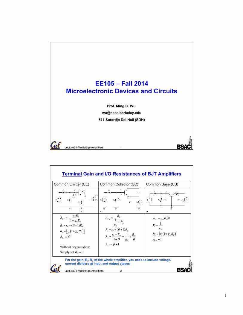
3 Lecture21-Multistage Amplifiers
Terminal Gain and I/O Resistances of MOS Amplifiers
AV ,t = −gmRL
1+ gmRSRi =∞
Ro = ro 1+ gmRE( )#$ %&
AI ,t =∞
Without degeneration:Simply set RS = 0
AV ,t =RL1gm
+ RL
Ri =∞
Ro =1gm
AI ,t =∞
AV ,t = gmRL
Ri =1gm
Ro = ro 1+ gmRE( )!" #$
AI ,t ≈1
For the gain, Ri, Ro of the whole amplifier, you need to include voltage/current dividers at input and output stages
Common Source (CS) Common Drain (CD) Common Gate (CG)
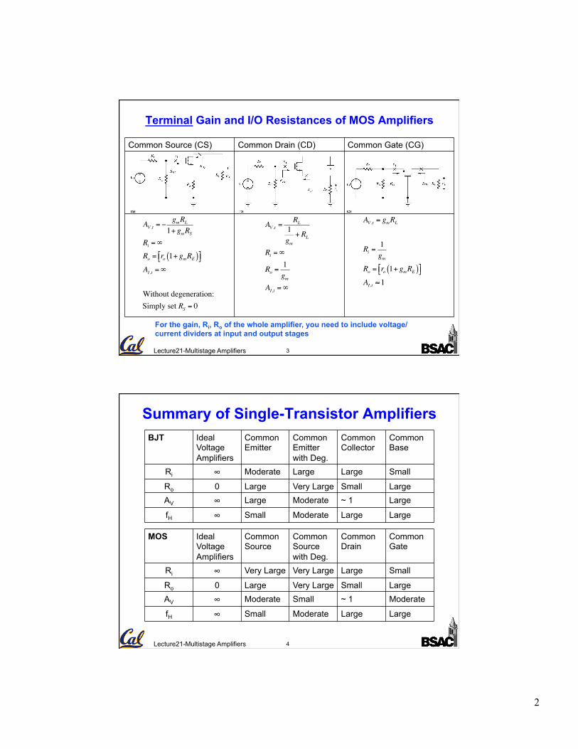
4 Lecture21-Multistage Amplifiers
Summary of Single-Transistor Amplifiers BJT Ideal
Voltage Amplifiers
Common Emitter
Common Emitter with Deg.
Common Collector
Common Base
Ri ∞ Moderate Large Large Small
Ro 0 Large Very Large Small Large AV ∞ Large Moderate ~ 1 Large
fH ∞ Small Moderate Large Large
MOS Ideal Voltage Amplifiers
Common Source
Common Source with Deg.
Common Drain
Common Gate
Ri ∞ Very Large Very Large Large Small
Ro 0 Large Very Large Small Large AV ∞ Moderate Small ~ 1 Moderate
fH ∞ Small Moderate Large Large
3
5 Lecture21-Multistage Amplifiers
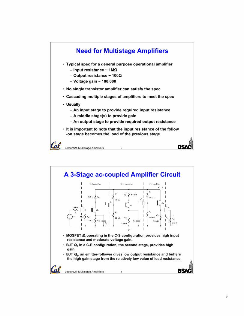
Need for Multistage Amplifiers
• Typical spec for a general purpose operational amplifier – Input resistance ~ 1MΩ – Output resistance ~ 100Ω – Voltage gain ~ 100,000
• No single transistor amplifier can satisfy the spec
• Cascading multiple stages of amplifiers to meet the spec
• Usually – An input stage to provide required input resistance – A middle stage(s) to provide gain – An output stage to provide required output resistance
• It is important to note that the input resistance of the follow-on stage becomes the load of the previous stage
6 Lecture21-Multistage Amplifiers
A 3-Stage ac-coupled Amplifier Circuit
• MOSFET M1operating in the C-S configuration provides high input resistance and moderate voltage gain.
• BJT Q2 in a C-E configuration, the second stage, provides high gain.
• BJT Q3, an emitter-follower gives low output resistance and buffers the high gain stage from the relatively low value of load resistance.
4
7 Lecture21-Multistage Amplifiers
A 3-Stage ac-coupled Amplifier Circuit
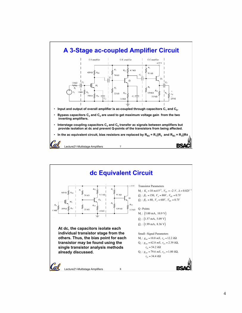
• Input and output of overall amplifier is ac-coupled through capacitors C1 and C6.
• Bypass capacitors C2 and C4 are used to get maximum voltage gain from the two inverting amplifiers.
• Interstage coupling capacitors C3 and C5 transfer ac signals between amplifiers but provide isolation at dc and prevent Q-points of the transistors from being affected.
• In the ac equivalent circuit, bias resistors are replaced by RB2 = R1||R2 and RB3 = R3||R4
8 Lecture21-Multistage Amplifiers
dc Equivalent Circuit
At dc, the capacitors isolate each individual transistor stage from the others. Thus, the bias point for each transistor may be found using the single transistor analysis methods already discussed.
€
Transistor Parameters
M1 : Kn =10 mA/V 2 , VTN = −2 V , λ = 0.02V −1
Q2 : βF =150, VA = 80V , VBE = 0.7V
Q3 : βF = 80, VA = 60V , VBE = 0.7V
Q - Points
M1 : 5.00 mA, 10.9 V( )Q2 : 1.57 mA, 5.09 V( )Q3 : 1.99 mA, 8.36 V( )
Small - Signal Parameters
M1 : gm1 =10.0 mS , ro1 =12.2 kΩ
Q2 : gm2 = 62.8 mS , rπ2 = 2.39 kΩ,
ro2 = 54.2 kΩ
Q3 : gm3 = 79.6 mS , rπ3 =1.00 kΩ,
ro3 = 34.4 kΩ

5
9 Lecture21-Multistage Amplifiers
ac and Small-Signal Equivalent Circuits
Small-signal Equivalent
ac Equivalent
10 Lecture21-Multistage Amplifiers
Input Resistance and Voltage Gain
RI1 = 620Ω 17.2kΩ = 598Ω
RI 2 = 4.7kΩ 51.8Ω = 4.31kΩ
RI3 = 3.3kΩ 250Ω = 232Ω
RL1 = RI1 Rin2 = 598Ω rπ 2 =598Ω 2390Ω = 478Ω
Rin = RG =1MΩ
€
Av = Avt3 Avt2 Avt1
Rin
RI + Rin
Avt1 =v2
v1
= −gm1RL1 = −0.01S 0.478kΩ( ) = −4.78
v1 = vi
Rin
RI + Rin
= vi
1MΩ10kΩ+1MΩ
= 0.990vi
RL2 = RI 2 Rin3 = RI 2 rπ 3 + βo3 +1( )RL3[ ] =3.54kΩ
Avt2 =v3
v2
= −gm2RL2 = −62.8S 3.54kΩ( ) = −222
Avt3 =vo
v3
=βo3 +1( )RL3
rπ 3 + βo3 +1( )RL3
= 0.950
Av = Avt3 Avt2 Avt1
RG
RI + RG
= +998
6
11 Lecture21-Multistage Amplifiers
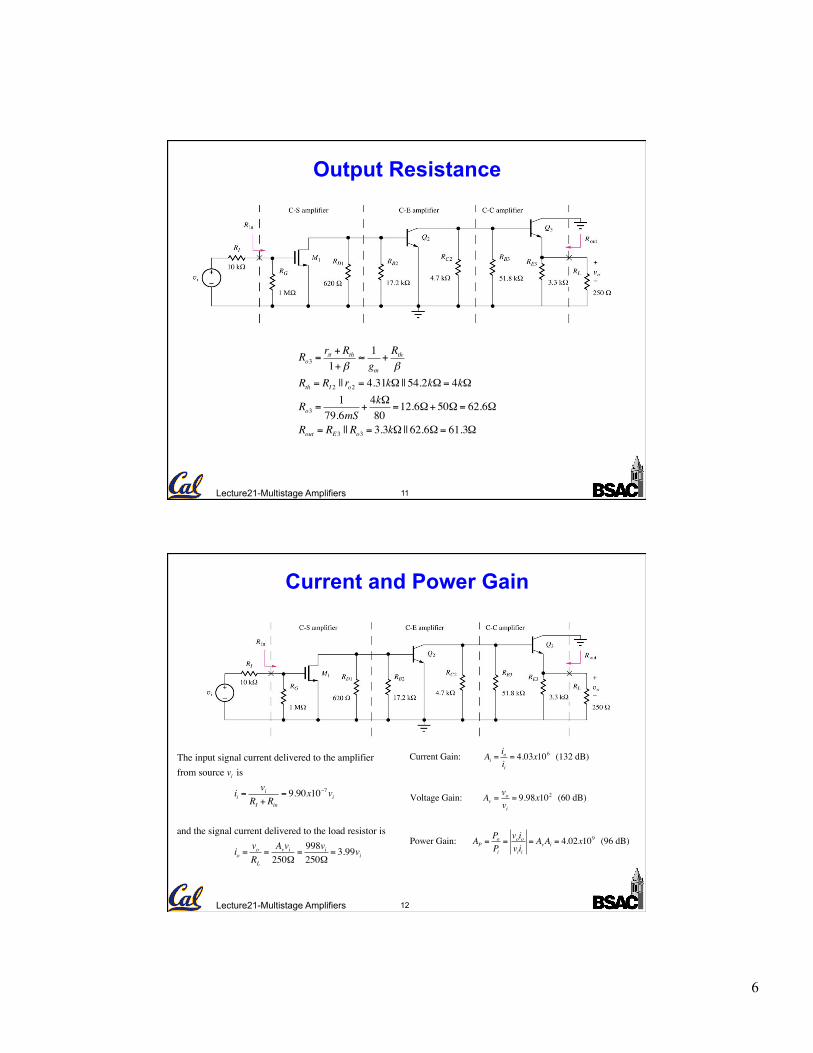
Output Resistance
Ro3 =rπ + Rth1+β
≈1gm
+Rthβ
Rth = RI 2 || ro2 = 4.31kΩ || 54.2kΩ = 4kΩ
Ro3 =1
79.6mS+4kΩ80
=12.6Ω+ 50Ω = 62.6Ω
Rout = RE3 || Ro3 = 3.3kΩ || 62.6Ω = 61.3Ω
12 Lecture21-Multistage Amplifiers
Current and Power Gain
Current Gain: Ai =ioii= 4.03x10⁶ (132 dB)
Voltage Gain: Av =vovi= 9.98x10² (60 dB)
Power Gain: AP =PoPi=voioviii
= AvAi = 4.02x10⁹ (96 dB)
The input signal current delivered to the amplifier from source vi is
ii =vi
RI + Rin= 9.90x10⁻⁷vi
and the signal current delivered to the load resistor is
io =voRL
=Avvi
250Ω=
998vi250Ω
= 3.99vi

7
13 Lecture21-Multistage Amplifiers
Input and Output Signal Range
For the first stage: v1 ≤ 0.2 VGS −VTN( ) → vi ≤0.2 −1+ 2( )V
0.99= 0.202 V
For the second stage: vbe2 = v2 = Av1v1 ≤ 5mV
v1 ≤5mVAv1
=5mV4.78
=1.05mV → vi ≤1.05mV
0.99=1.06 mV
For the third stage: vbe3 ≅v3
1+ gm3RL3
=Av1Av2 0.990vi( )
1+ gm3RL3
≤ 5mV
vi ≤1+ gm3RL3
Av1Av2 0.990( )5mV = 92.7 µV
Overall: vi ≤min 202mV,1.06mV, 92.7µV( ) = 92.7µV
vo ≤ Av 92.7µV( ) = 998 92.7µV( ) = 92.5 mV
14 Lecture21-Multistage Amplifiers
SPICE Simulation Circuit
8
15 Lecture21-Multistage Amplifiers
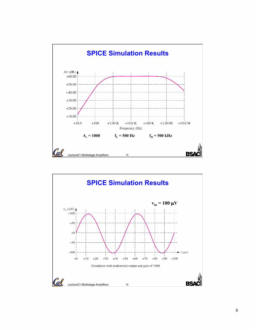
SPICE Simulation Results
Av = 1000 fL = 500 Hz fH = 500 kHz
16 Lecture21-Multistage Amplifiers
SPICE Simulation Results
vin = 100 µV

9
17 Lecture21-Multistage Amplifiers
SPICE Simulation Results
vin = 750 µV
18 Lecture21-Multistage Amplifiers
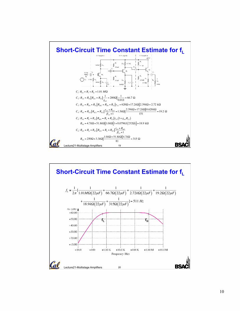
Short-Circuit Time Constant Estimate for fL
An estimate for the lower cutoff frequency for an amplifier with multiple coupling and bypass capacitors is given by the sum of the reciprocals of the "short-circuit" time constants:
fL ≅1
2π1
RiSCii=1
n
∑
where RiS is the resistance at the terminals of the ith capacitor with all the other capacitors shorted.
10
19 Lecture21-Multistage Amplifiers
Short-Circuit Time Constant Estimate for fL
C1: R1S = RI + RG =1.01 MΩ
C2: R2S = RS1 RiS1 = RS11gm1
= 200Ω 10.01S
= 66.7 Ω
C3: R3S = RD1 + RI1 RiB2 = RD1 + RI1 rπ 2 = 620Ω+17.2kΩ 2.39kΩ = 2.72 kΩ
C4: R4S = RE2 RiE2 = RE2rπ 2 + Rth2
βo2 +1=1.5kΩ
2.39kΩ+17.2kΩ 0.620kΩ151
=19.2 Ω
C5: R5S = RC + RI 2 RiB3 = RL + RI 2 rπ 3 1+ gm3RL3( ) R5S = 4.7kΩ+ 51.8kΩ 1.0kΩ 1+ 0.0796S 232Ω( )"# $%=18.9 kΩ
C6: R6S = RL + RE3 RiE3 = RL + RE3rπ 3 + Rth3
βo3 +1
R6S = 250Ω+3.3kΩ1.0kΩ+ 51.8kΩ 4.7kΩ
81= 315 Ω
20 Lecture21-Multistage Amplifiers
Short-Circuit Time Constant Estimate for fL
fL ≅1
2π[ 11.01MΩ 22µF( )
+1
66.7Ω 22µF( )+
12.72kΩ 22µF( )
+1
19.2Ω 22µF( )
+ 118.9kΩ 22µF( )
+1
315Ω 22µF( )]= 511 Hz
fL fH