ECE615 Mixed-Signal IC Design - University of Delaware
57
Department of Electrical and Computer Engineering © Vishal Saxena -1- Aug 27, 2013 ECE615 Mixed-Signal IC Design Vishal Saxena ([email protected]) Analog Mixed Signal IC Laboratory Boise State University Discrete-Time ΔΣ Modulator Implementation
Transcript of ECE615 Mixed-Signal IC Design - University of Delaware
Department of Electrical and Computer Engineering
© Vishal Saxena -1- Aug 27, 2013
ECE615 Mixed-Signal IC Design
Vishal Saxena
Analog Mixed Signal IC Laboratory
Boise State University
Discrete-Time ΔΣ Modulator
Implementation
© Vishal Saxena -2- Aug 27, 2013
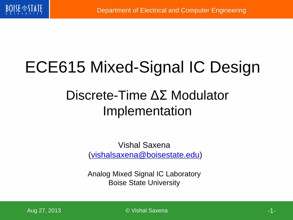
Review: A ΔΣ ADC System
© Vishal Saxena -3- Aug 27, 2013
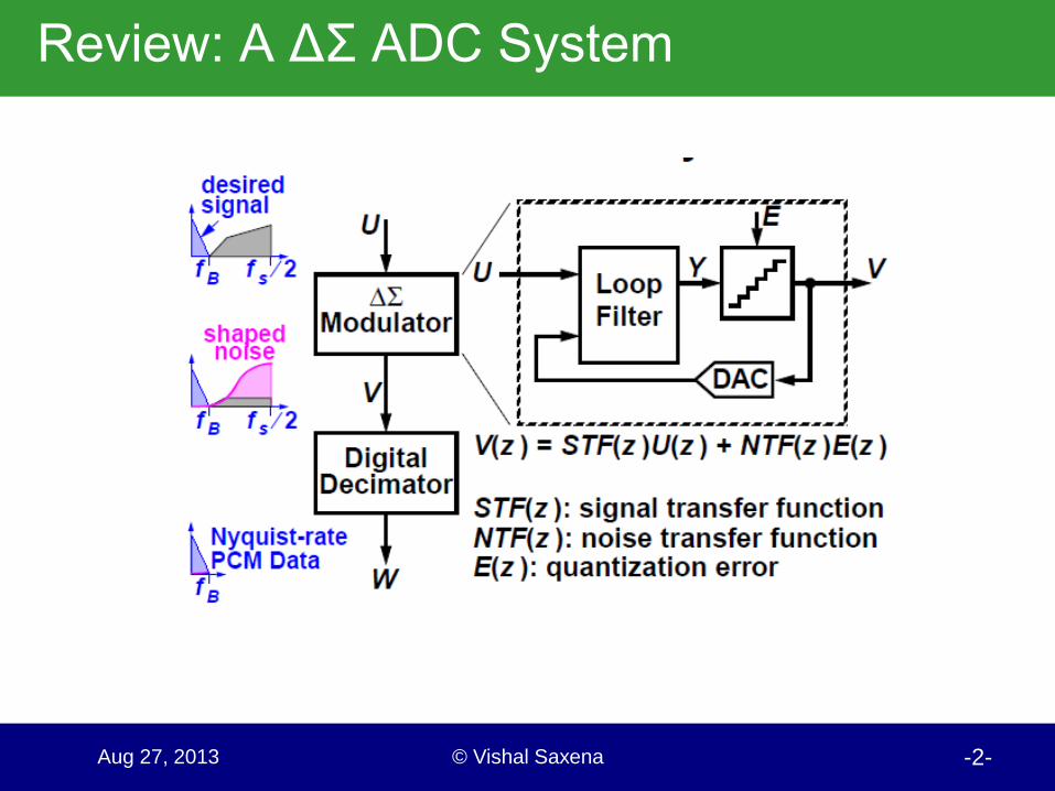
Review: MOD1
© Vishal Saxena -4- Aug 27, 2013
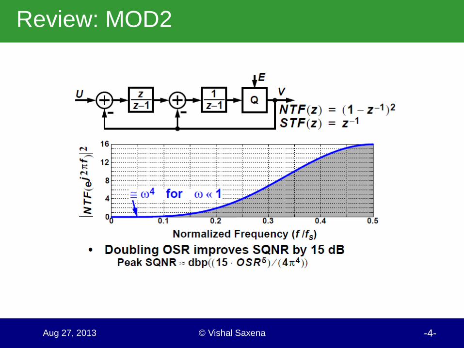
Review: MOD2
© Vishal Saxena -5- Aug 27, 2013
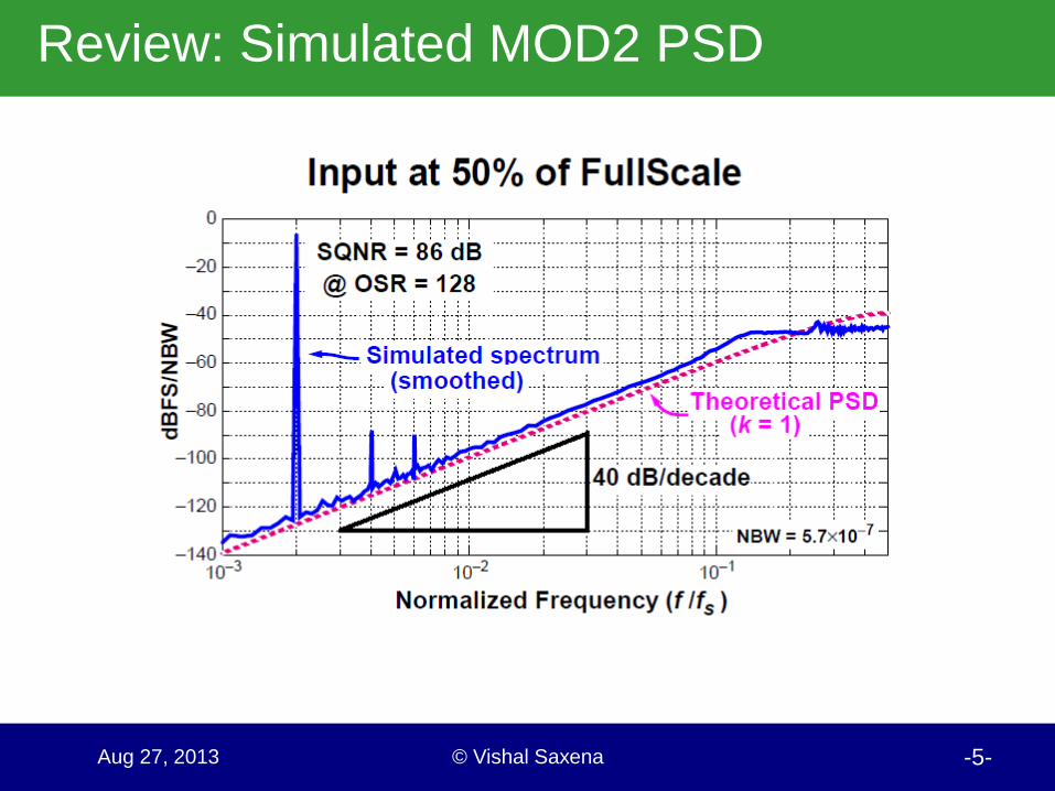
Review: Simulated MOD2 PSD
© Vishal Saxena -6- Aug 27, 2013
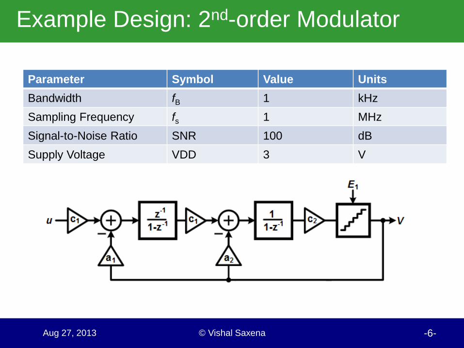
Example Design: 2nd-order Modulator
Parameter Symbol Value Units
Bandwidth fB 1 kHz
Sampling Frequency fs 1 MHz
Signal-to-Noise Ratio SNR 100 dB
Supply Voltage VDD 3 V
© Vishal Saxena -7- Aug 27, 2013
NTF Design
7
© Vishal Saxena -8- Aug 27, 2013
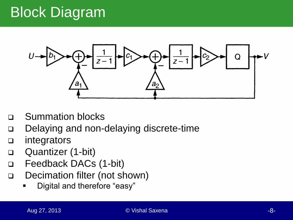
Block Diagram
Summation blocks
Delaying and non-delaying discrete-time
integrators
Quantizer (1-bit)
Feedback DACs (1-bit)
Decimation filter (not shown) Digital and therefore “easy”
© Vishal Saxena -9- Aug 27, 2013
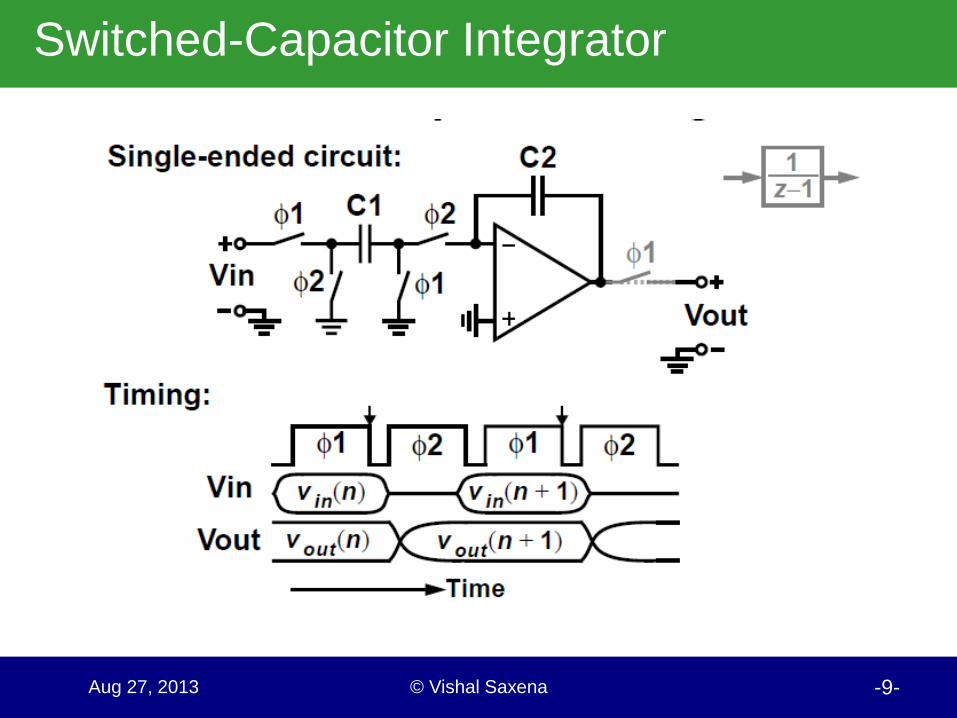
Switched-Capacitor Integrator

© Vishal Saxena -10- Aug 27, 2013
Switched-Capacitor Integrator contd.
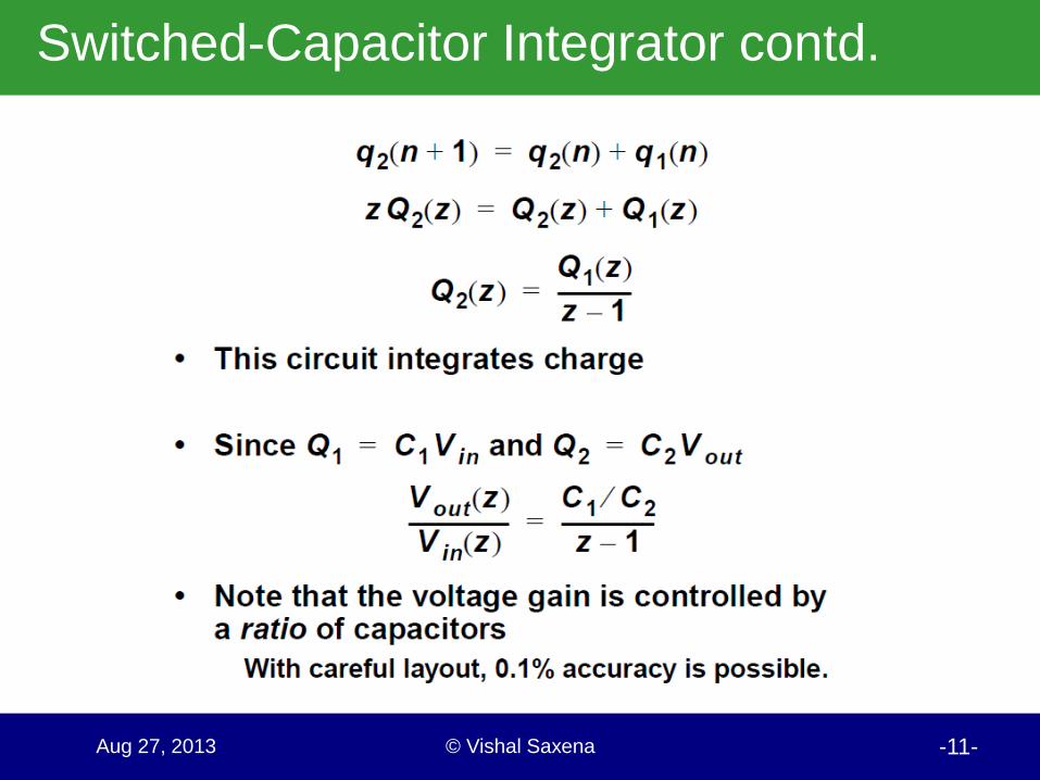
© Vishal Saxena -11- Aug 27, 2013
Switched-Capacitor Integrator contd.
© Vishal Saxena -12- Aug 27, 2013
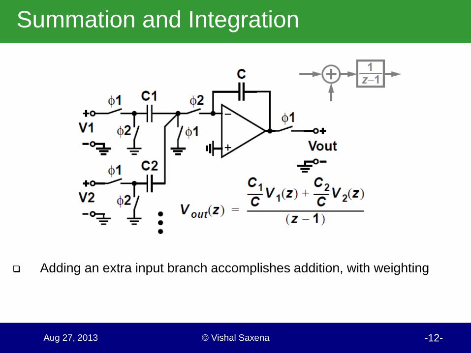
Summation and Integration
Adding an extra input branch accomplishes addition, with weighting
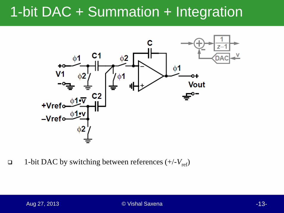
© Vishal Saxena -13- Aug 27, 2013
1-bit DAC + Summation + Integration
1-bit DAC by switching between references (+/-Vref)

© Vishal Saxena -14- Aug 27, 2013
Fully-Differential Integrator
© Vishal Saxena -15- Aug 27, 2013
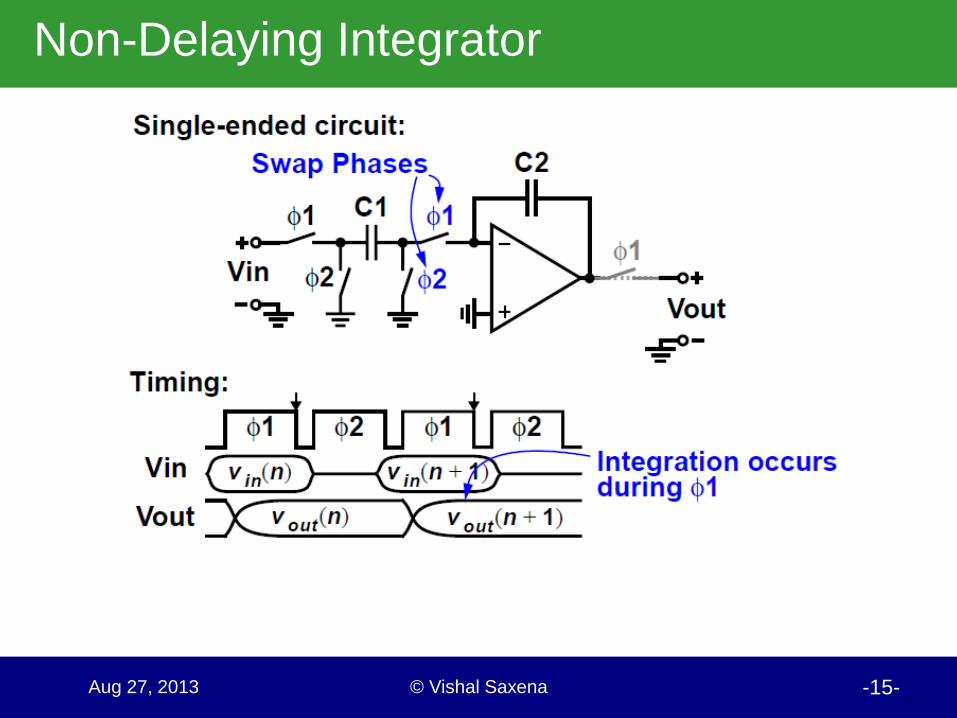
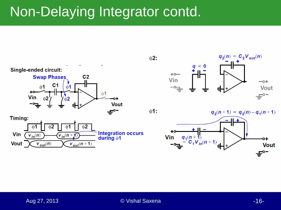
Non-Delaying Integrator
© Vishal Saxena -16- Aug 27, 2013
Non-Delaying Integrator contd.
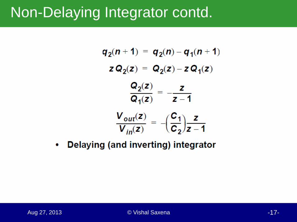
© Vishal Saxena -17- Aug 27, 2013
Non-Delaying Integrator contd.
© Vishal Saxena -18- Aug 27, 2013
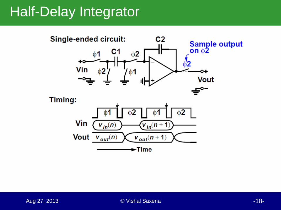
Half-Delay Integrator
© Vishal Saxena -19- Aug 27, 2013
Half-Delay Integrator
Output is sampled on a different phase than the input
Some use the notation to denote the shift in sampling time
An alternative method is to declare that the border between time n and n+1 occurs at the end of a specific phase, say φ2
A circuit which samples on φ1 and updates on φ2 is non-delaying, i.e. H(z) = z ⁄ (z – 1)
whereas a circuit which samples on φ2 and updates on φ1 is delaying, i.e. H(z) = 1 ⁄ (z – 1)
© Vishal Saxena -20- Aug 27, 2013
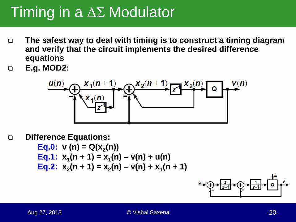
Timing in a ΔΣ Modulator
The safest way to deal with timing is to construct a timing diagram and verify that the circuit implements the desired difference equations
E.g. MOD2:
Difference Equations:
Eq.0: v (n) = Q(x2(n))
Eq.1: x1(n + 1) = x1(n) – v(n) + u(n)
Eq.2: x2(n + 1) = x2(n) – v(n) + x1(n + 1)
© Vishal Saxena -21- Aug 27, 2013
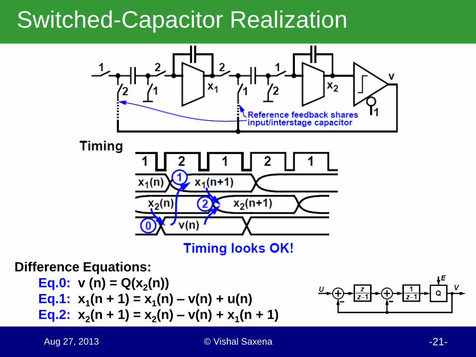
Switched-Capacitor Realization
Difference Equations:
Eq.0: v (n) = Q(x2(n))
Eq.1: x1(n + 1) = x1(n) – v(n) + u(n)
Eq.2: x2(n + 1) = x2(n) – v(n) + x1(n + 1)
© Vishal Saxena -22- Aug 27, 2013
Signal Swing
So far, we have not paid any attention to how much linear swing the op
amps can support, or to the magnitudes of u, Vref, x1 and x2
For simplicity, assume:
the full-scale range of u is +/-1V
the opamp swing is also +/-1V and
Vref = +/-1V
We still need to know the ranges of x1 and x2 in order to accomplish
dynamic-range scaling
© Vishal Saxena -23- Aug 27, 2013
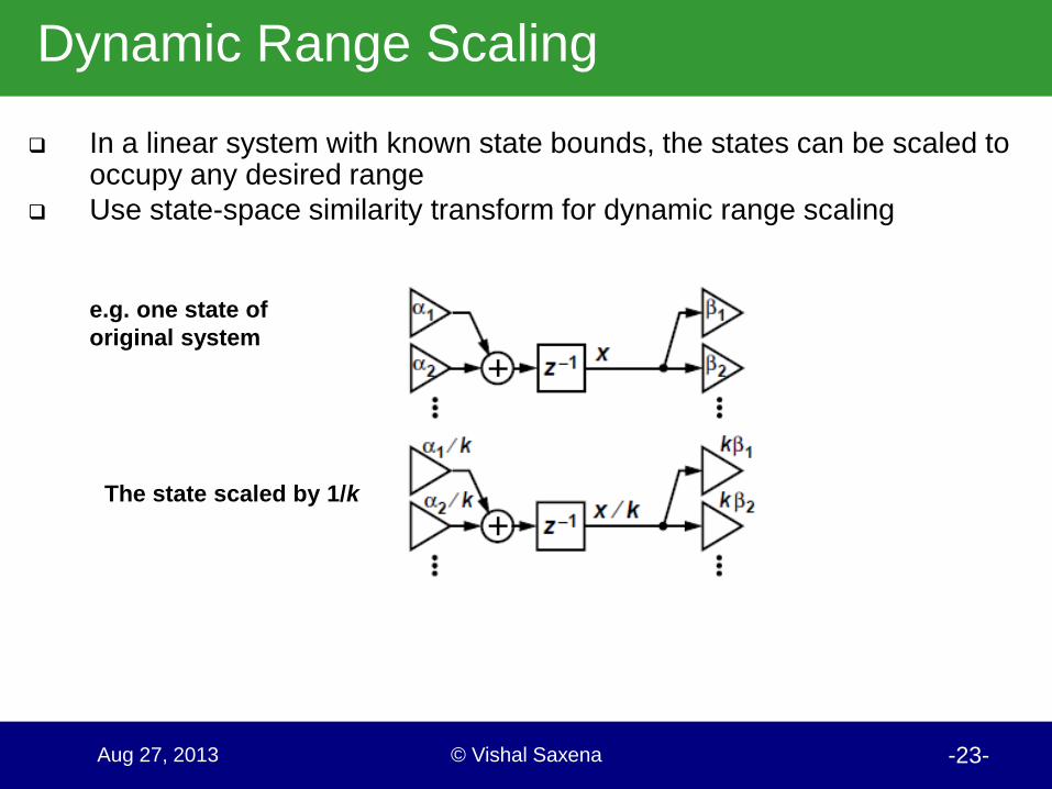
Dynamic Range Scaling
In a linear system with known state bounds, the states can be scaled to occupy any desired range
Use state-space similarity transform for dynamic range scaling
e.g. one state of
original system
The state scaled by 1/k
© Vishal Saxena -24- Aug 27, 2013
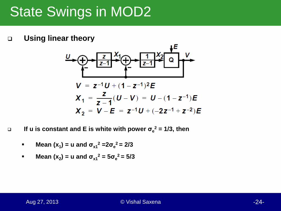
State Swings in MOD2
Using linear theory
If u is constant and E is white with power σe2 = 1/3, then
Mean (x1) = u and σx12 =2σe
2 = 2/3
Mean (x2) = u and σx12 = 5σe
2 = 5/3
© Vishal Saxena -25- Aug 27, 2013
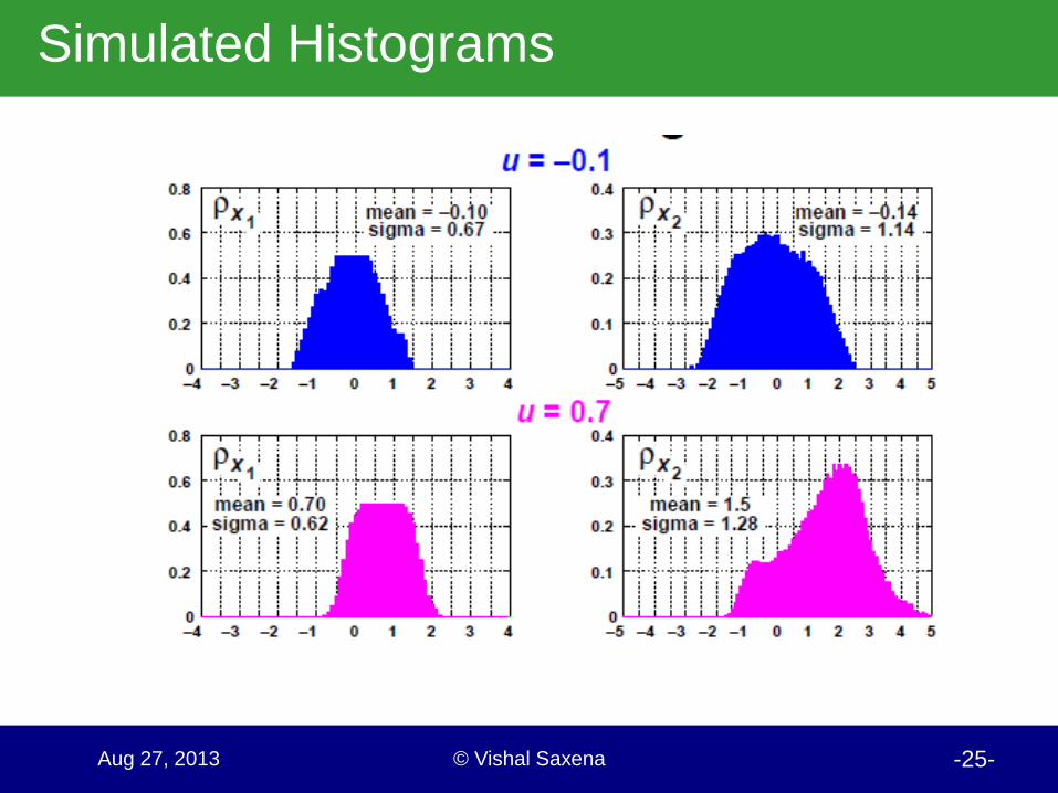
Simulated Histograms
© Vishal Saxena -26- Aug 27, 2013
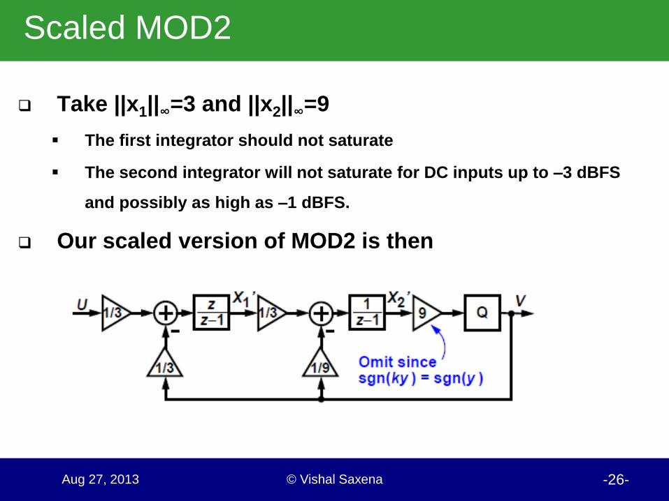
Scaled MOD2
Take ||x1||∞=3 and ||x2||∞=9
The first integrator should not saturate
The second integrator will not saturate for DC inputs up to –3 dBFS
and possibly as high as –1 dBFS.
Our scaled version of MOD2 is then
© Vishal Saxena -27- Aug 27, 2013
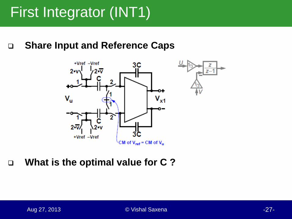
First Integrator (INT1)
Share Input and Reference Caps
What is the optimal value for C ?
© Vishal Saxena -28- Aug 27, 2013
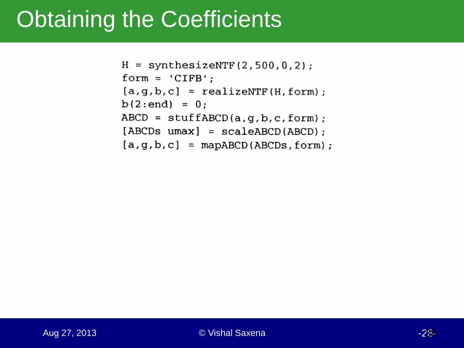
Obtaining the Coefficients
28
© Vishal Saxena -29- Aug 27, 2013
Voltage Scaling from the Toolbox
Translation of toolbox block diagram to a practical circuit.
Toolbox assumes the input of a single-bit modulator ranges from -1 to +1
The default DRS is also such that the integrator states occupy the [-1,1] range
The toolbox quantizer LSB size is 2 units
However, in analog circuits the range must have physical units and
match the voltage limits set by the technology
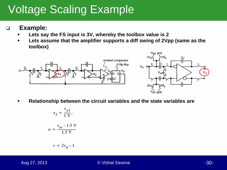
Example:
Lets say the FS input is 3V, whereby the toolbox value is 2
Lets assume that the amplifier supports a diff swing of 2Vpp (same as the
toolbox)
© Vishal Saxena -30- Aug 27, 2013
Voltage Scaling Example
Example: Lets say the FS input is 3V, whereby the toolbox value is 2
Lets assume that the amplifier supports a diff swing of 2Vpp (same as the
toolbox)
Relationship between the circuit variables and the state variables are
© Vishal Saxena -31- Aug 27, 2013
Voltage Scaling Example contd.
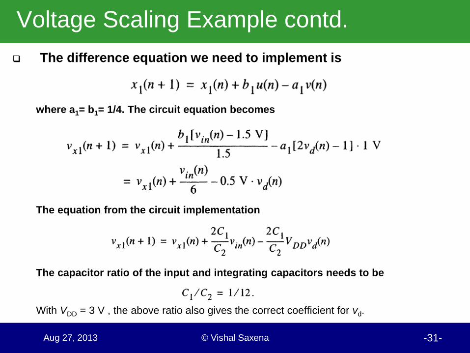
The difference equation we need to implement is
where a1= b1= 1/4. The circuit equation becomes
The equation from the circuit implementation
The capacitor ratio of the input and integrating capacitors needs to be
With VDD = 3 V , the above ratio also gives the correct coefficient for vd.
© Vishal Saxena -32- Aug 27, 2013
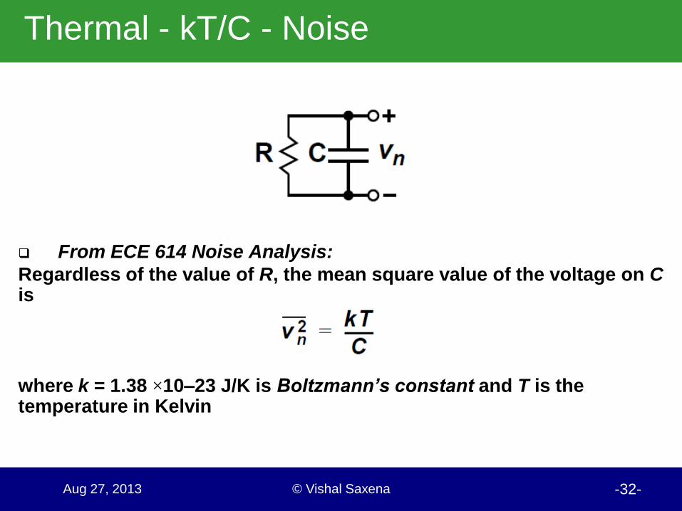
Thermal - kT/C - Noise
From ECE 614 Noise Analysis:
Regardless of the value of R, the mean square value of the voltage on C is
where k = 1.38 ×10⁻²³ J/K is Boltzmann’s constant and T is the temperature in Kelvin
© Vishal Saxena -33- Aug 27, 2013
Noise in SC Integrator
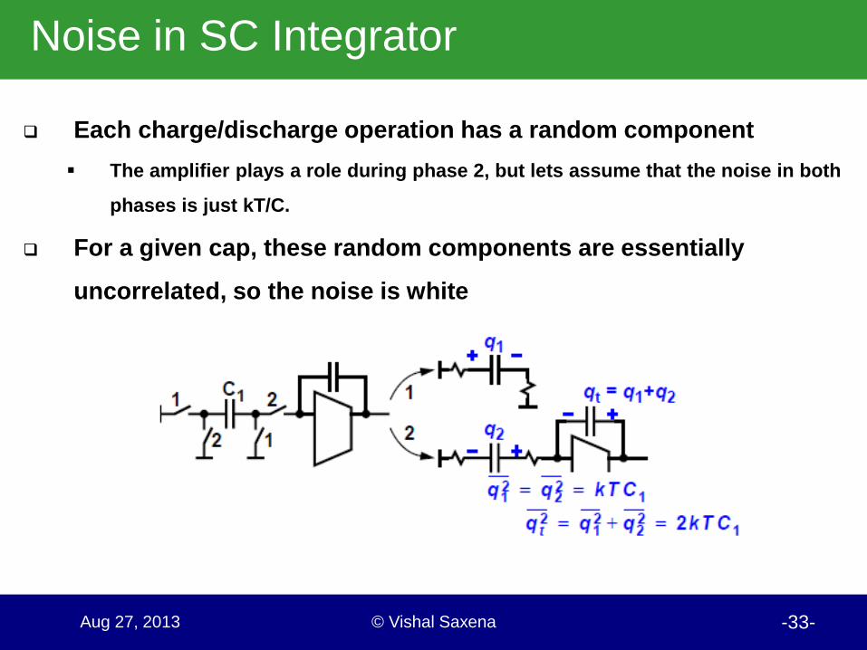
Each charge/discharge operation has a random component
The amplifier plays a role during phase 2, but lets assume that the noise in both
phases is just kT/C.
For a given cap, these random components are essentially
uncorrelated, so the noise is white
© Vishal Saxena -34- Aug 27, 2013
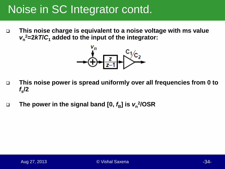
Noise in SC Integrator contd.
This noise charge is equivalent to a noise voltage with ms value vn
2=2kT/C1 added to the input of the integrator:
This noise power is spread uniformly over all frequencies from 0 to fs/2
The power in the signal band [0, fB] is vn2/OSR
© Vishal Saxena -35- Aug 27, 2013
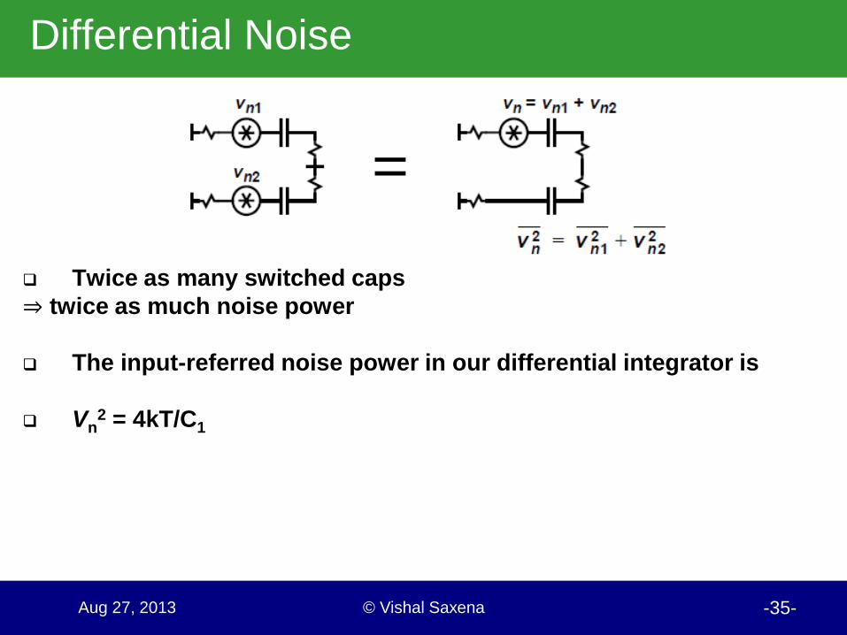
Differential Noise
Twice as many switched caps
⇒ twice as much noise power
The input-referred noise power in our differential integrator is
Vn2 = 4kT/C1
© Vishal Saxena -36- Aug 27, 2013
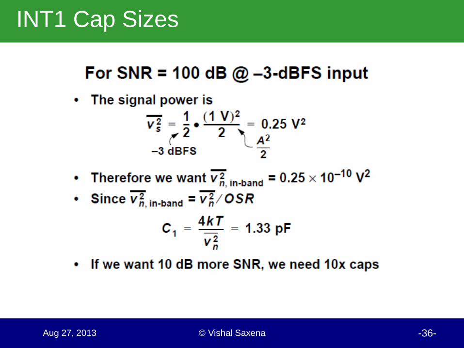
INT1 Cap Sizes
© Vishal Saxena -37- Aug 27, 2013
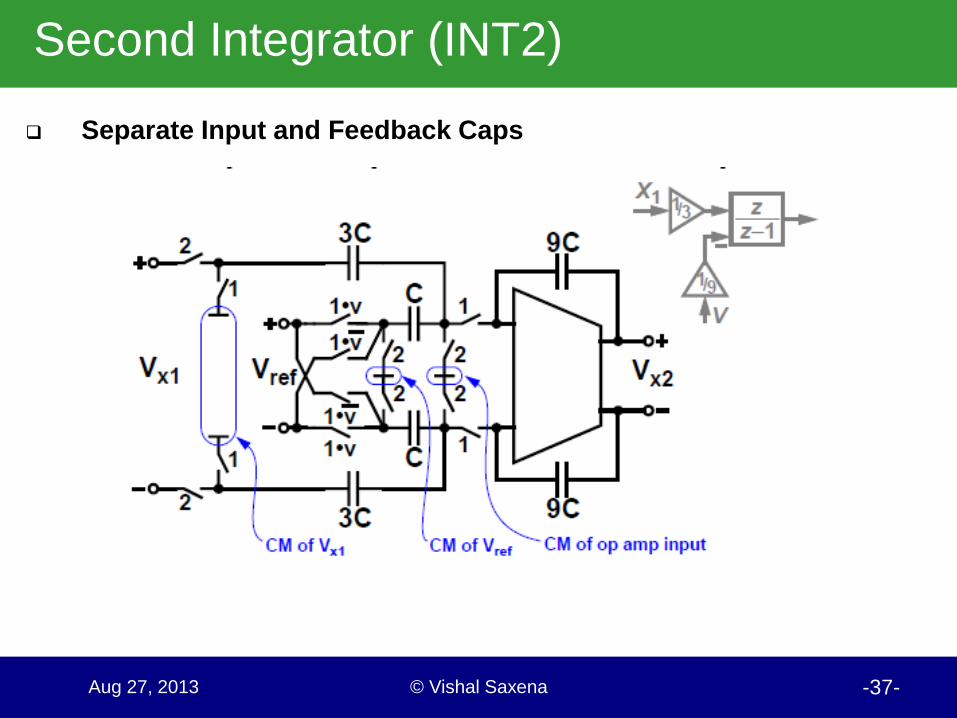
Second Integrator (INT2)
Separate Input and Feedback Caps
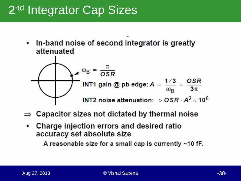
© Vishal Saxena -38- Aug 27, 2013
2nd Integrator Cap Sizes
© Vishal Saxena -39- Aug 27, 2013
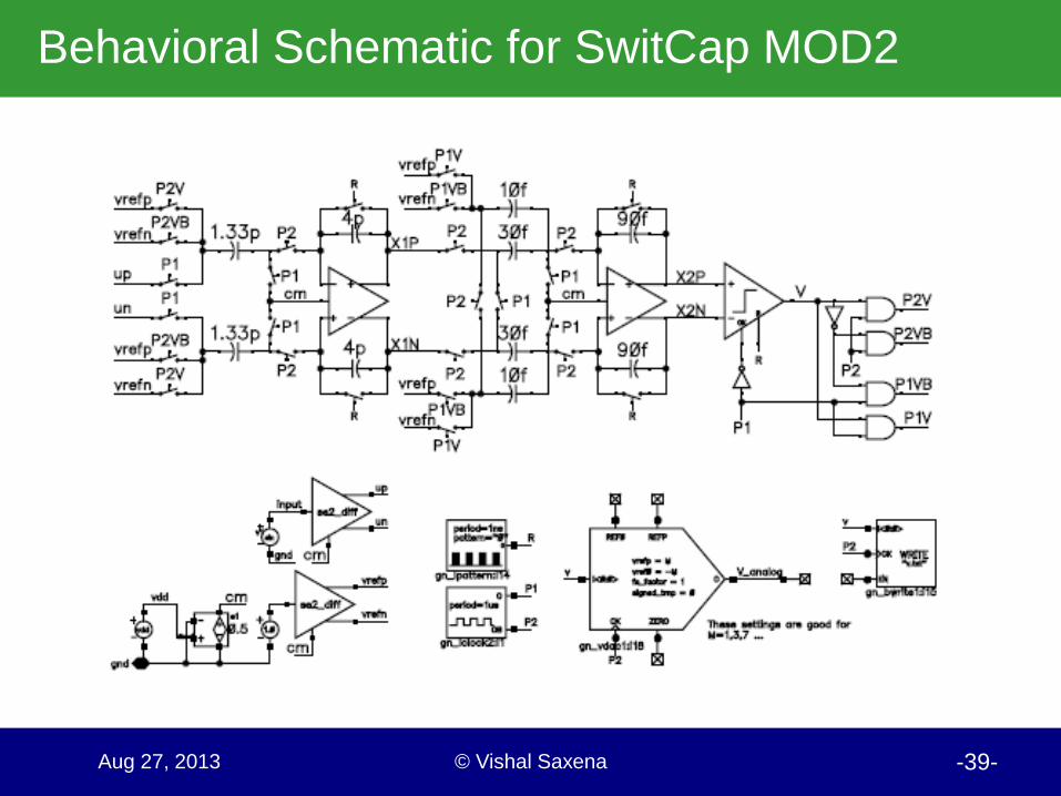
Behavioral Schematic for SwitCap MOD2
© Vishal Saxena -40- Aug 27, 2013
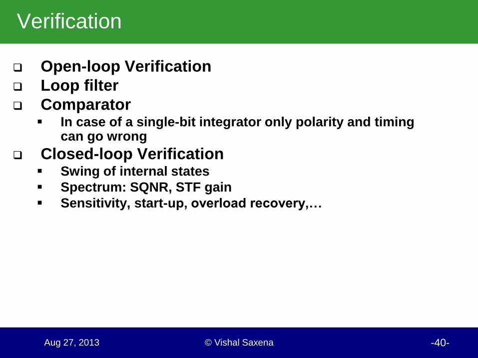
Verification
Open-loop Verification
Loop filter
Comparator In case of a single-bit integrator only polarity and timing
can go wrong
Closed-loop Verification Swing of internal states
Spectrum: SQNR, STF gain
Sensitivity, start-up, overload recovery,…
© Vishal Saxena -41- Aug 27, 2013
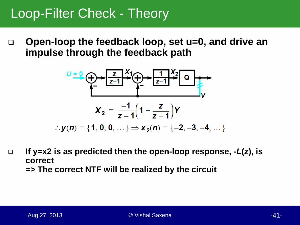
Loop-Filter Check - Theory
Open-loop the feedback loop, set u=0, and drive an impulse through the feedback path
If y=x2 is as predicted then the open-loop response, -L(z), is
correct => The correct NTF will be realized by the circuit
© Vishal Saxena -42- Aug 27, 2013
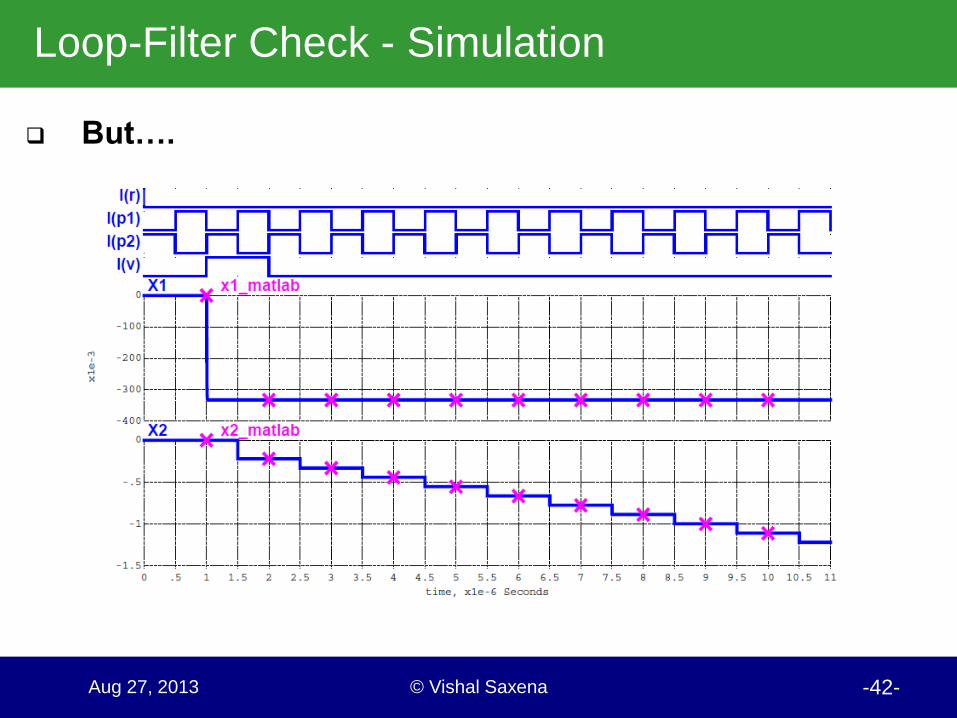
Loop-Filter Check - Simulation
But….
© Vishal Saxena -43- Aug 27, 2013
Loop-Filter Check - Specifics
An impulse response is {1,0,0,0}, but a binary DAC can only output +/-1 , i.e. it can’t produce a zero
Q: So how can we determine the impulse response of the loop filter through simulation?
A: Do two simulations: one with v={-1,-1,-1,….} and one with v={+1,-1,-1,…}.
Then take the difference.
According to linear superposition, the result is the response to v={2,0,0,…}, so divide by 2. To keep the integrator states from growing too quickly, one
could also use v={-1,-1,+1,-1,…} and then v={+1,-1,+1,-1,…}
© Vishal Saxena -44- Aug 27, 2013
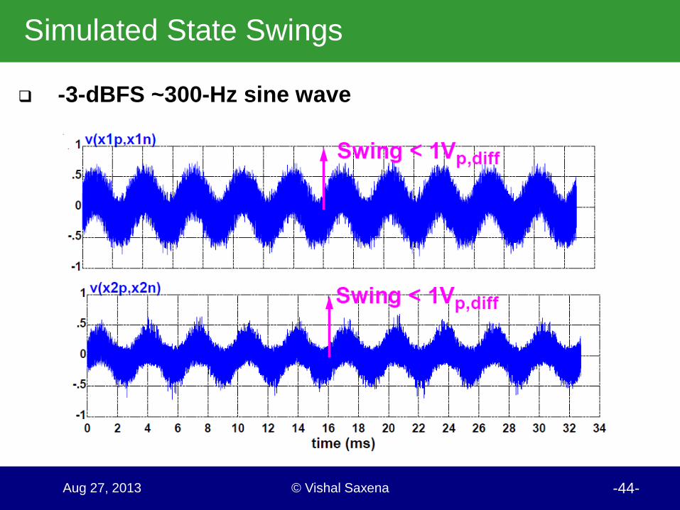
Simulated State Swings
-3-dBFS ~300-Hz sine wave
© Vishal Saxena -45- Aug 27, 2013
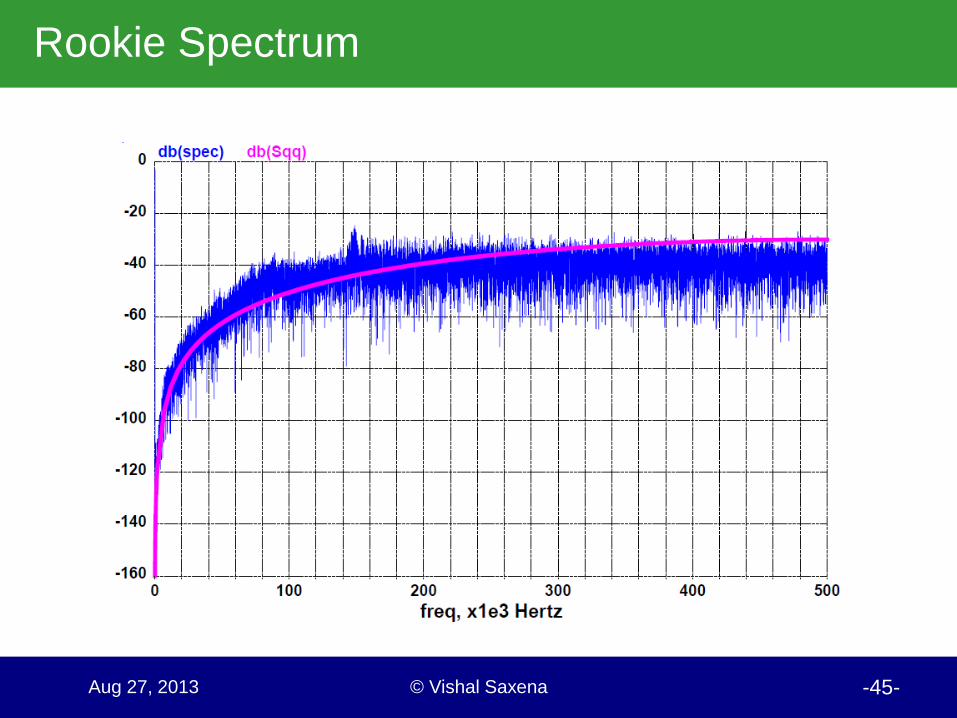
Rookie Spectrum
© Vishal Saxena -46- Aug 27, 2013
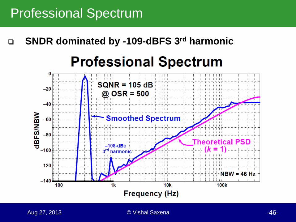
Professional Spectrum
SNDR dominated by -109-dBFS 3rd harmonic
© Vishal Saxena -47- Aug 27, 2013
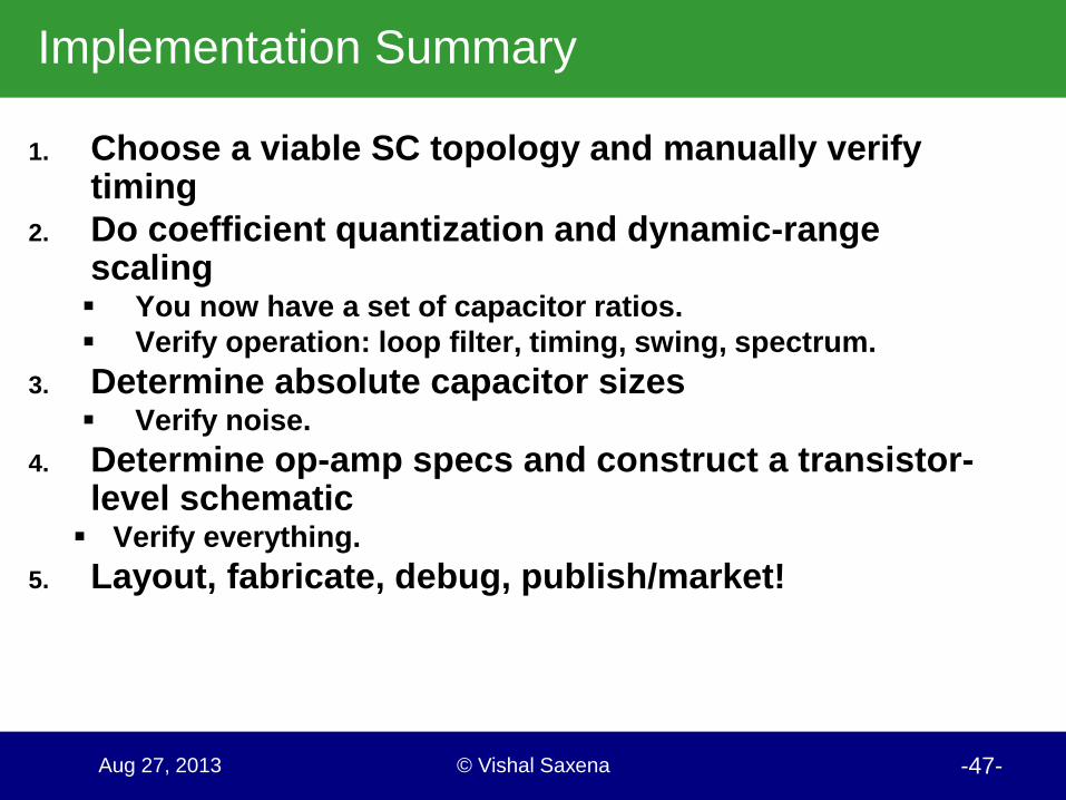
Implementation Summary
1. Choose a viable SC topology and manually verify timing
2. Do coefficient quantization and dynamic-range scaling You now have a set of capacitor ratios.
Verify operation: loop filter, timing, swing, spectrum.
3. Determine absolute capacitor sizes Verify noise.
4. Determine op-amp specs and construct a transistor-level schematic Verify everything.
5. Layout, fabricate, debug, publish/market!
© Vishal Saxena -48- Aug 27, 2013
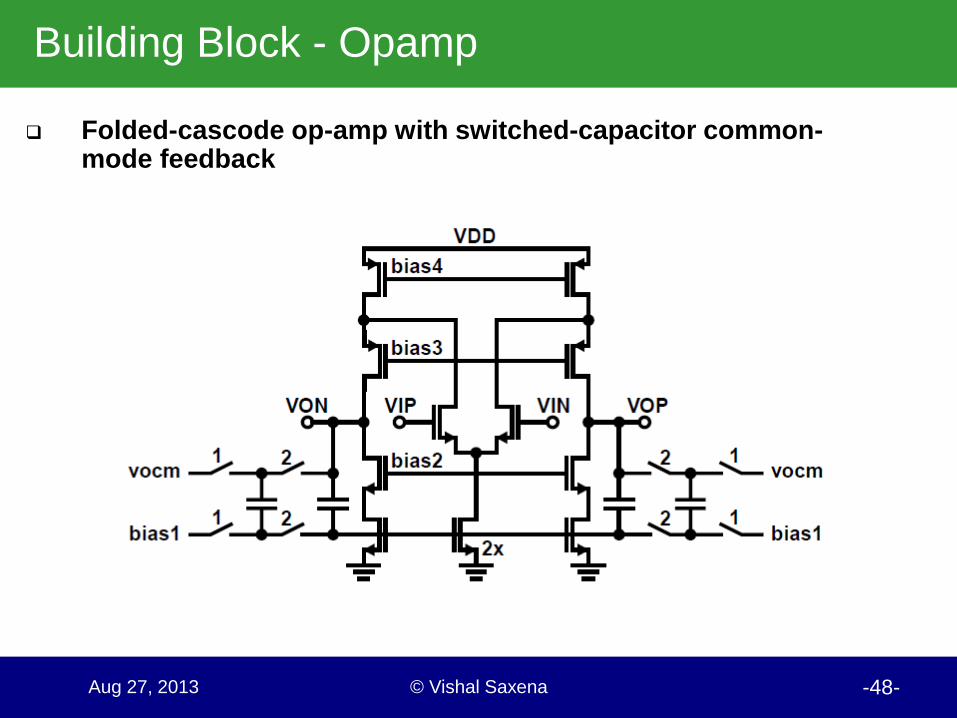
Building Block - Opamp
Folded-cascode op-amp with switched-capacitor common-mode feedback
© Vishal Saxena -49- Aug 27, 2013
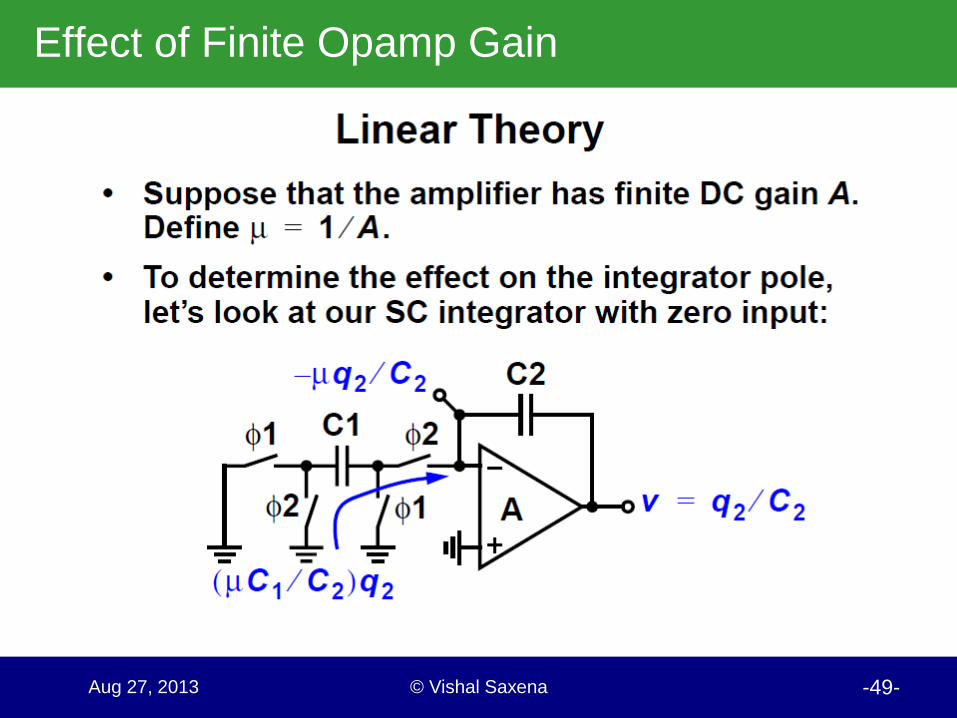
Effect of Finite Opamp Gain
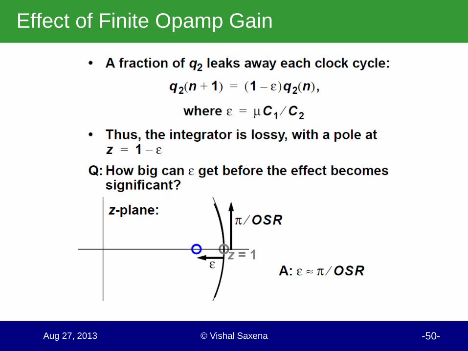
© Vishal Saxena -50- Aug 27, 2013
Effect of Finite Opamp Gain
© Vishal Saxena -51- Aug 27, 2013
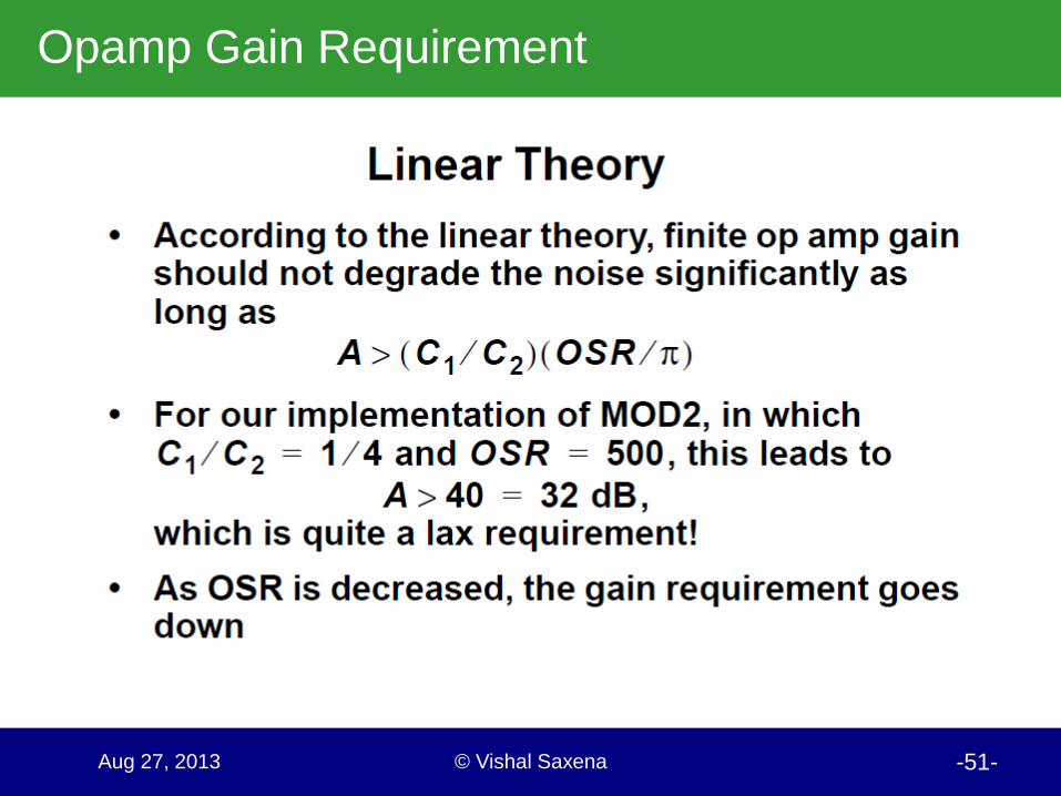
Opamp Gain Requirement
© Vishal Saxena -52- Aug 27, 2013
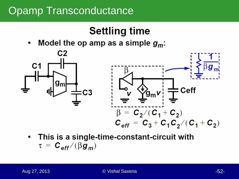
Opamp Transconductance
© Vishal Saxena -53- Aug 27, 2013
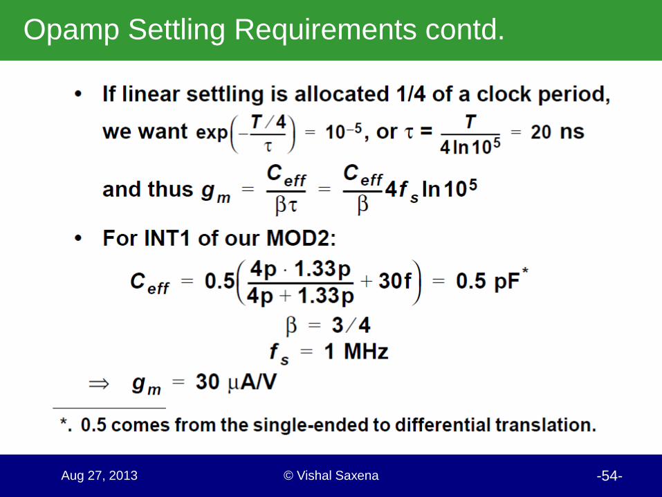
Opamp Settling Requirements
© Vishal Saxena -54- Aug 27, 2013
Opamp Settling Requirements contd.
© Vishal Saxena -55- Aug 27, 2013
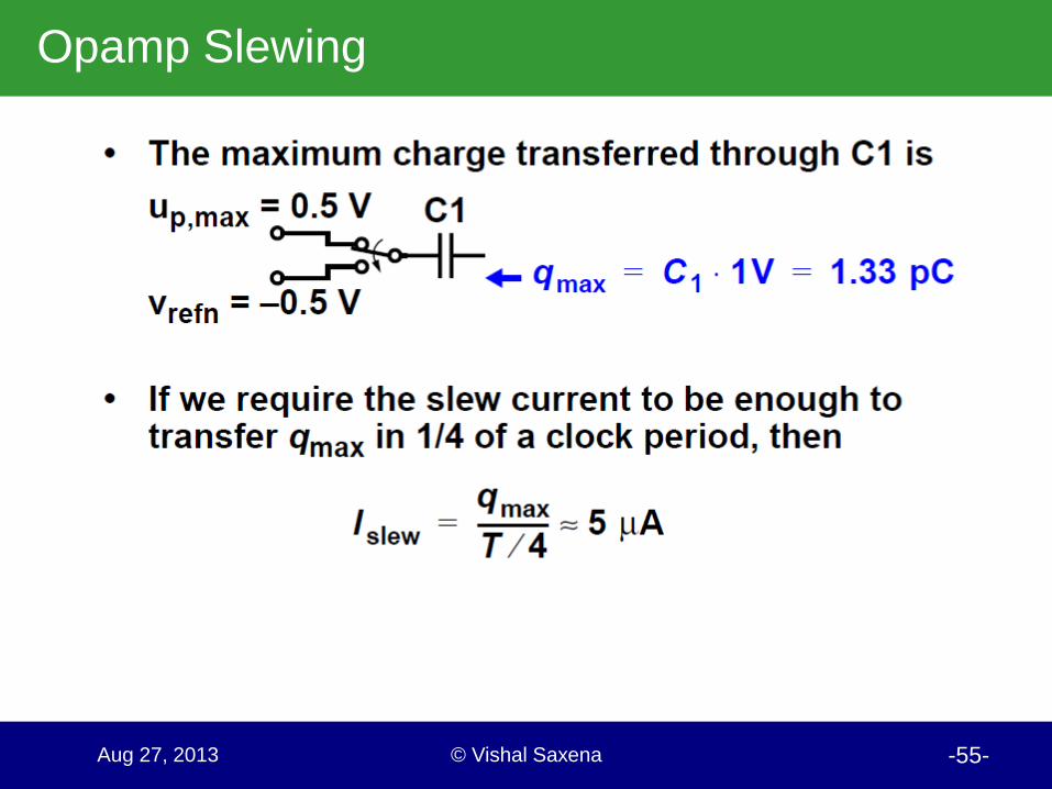
Opamp Slewing
© Vishal Saxena -56- Aug 27, 2013
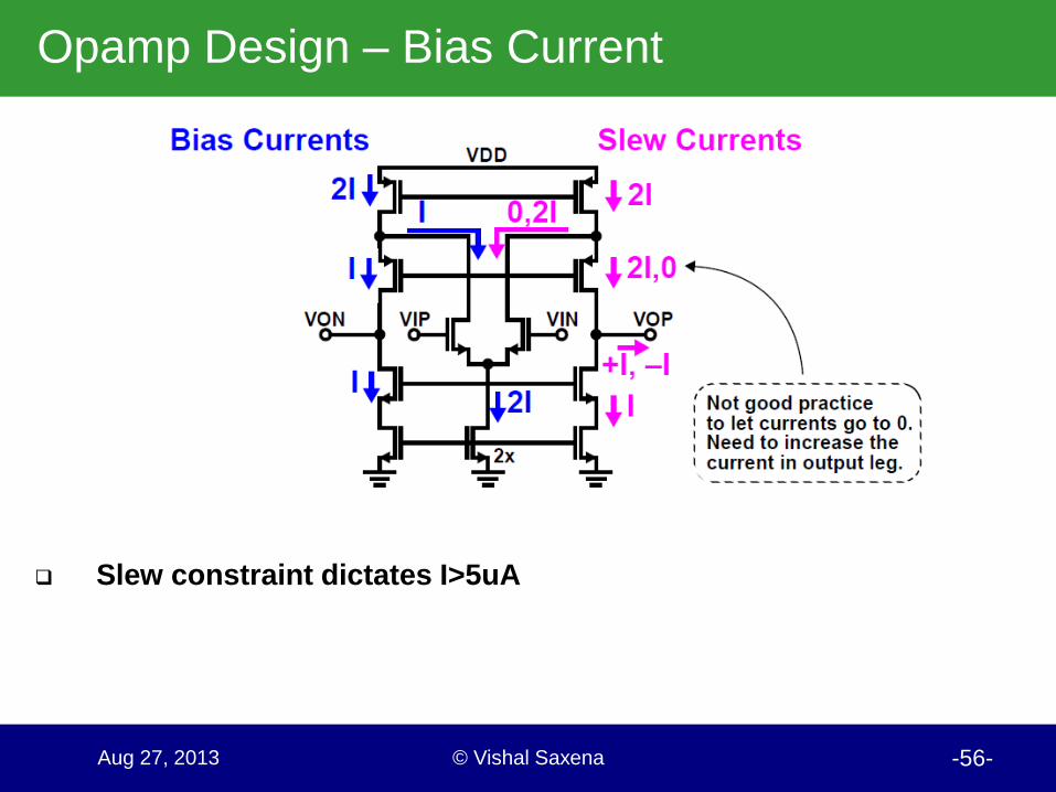
Opamp Design – Bias Current
Slew constraint dictates I>5uA
© Vishal Saxena -57- Aug 27, 2013