DWA Algorithm for Band-Pass ΔΣ DAC with Ternary Unit Cells · DWA Algorithm for Band-Pass ΔΣ...
45
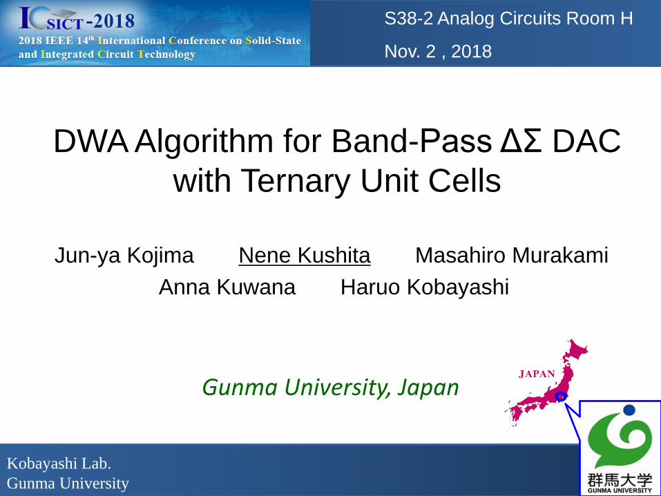
Kobayashi Lab. Gunma University Jun-ya Kojima Nene Kushita Masahiro Murakami Anna Kuwana Haruo Kobayashi DWA Algorithm for Band-Pass ΔΣ DAC with Ternary Unit Cells S38-2 Analog Circuits Room H Nov. 2 , 2018 Gunma University, Japan
Transcript of DWA Algorithm for Band-Pass ΔΣ DAC with Ternary Unit Cells · DWA Algorithm for Band-Pass ΔΣ...
Kobayashi Lab.
Gunma University
Jun-ya Kojima Nene Kushita Masahiro Murakami
Anna Kuwana Haruo Kobayashi
DWA Algorithm for Band-Pass ΔΣ DAC
with Ternary Unit Cells
S38-2 Analog Circuits Room H
Nov. 2 , 2018
Gunma University, Japan
2/42
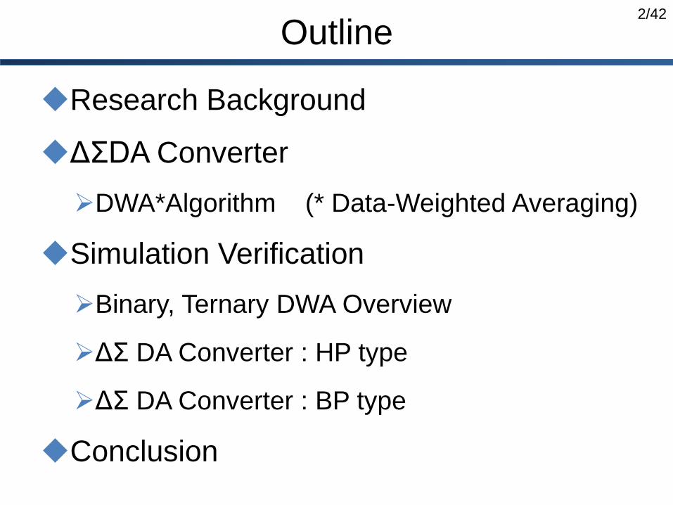
Outline
Research Background
ΔΣDA Converter
DWA*Algorithm (* Data-Weighted Averaging)
Simulation Verification
Binary, Ternary DWA Overview
ΔΣ DA Converter : HP type
ΔΣ DA Converter : BP type
Conclusion
3/42
Outline
Research Background
ΔΣDA Converter
DWA*Algorithm (* Data-Weighted Averaging)
Simulation Verification
Binary, Ternary DWA Overview
ΔΣ DA Converter : HP type
ΔΣ DA Converter : BP type
Conclusion
4/42
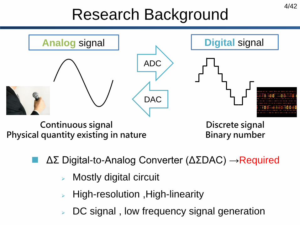
Research Background
ΔΣ Digital-to-Analog Converter (ΔΣDAC) →Required
Mostly digital circuit
High-resolution ,High-linearity
DC signal , low frequency signal generation
ADC
DAC
Analog signal Digital signal
Continuous signalPhysical quantity existing in nature
Discrete signalBinary number
5/42
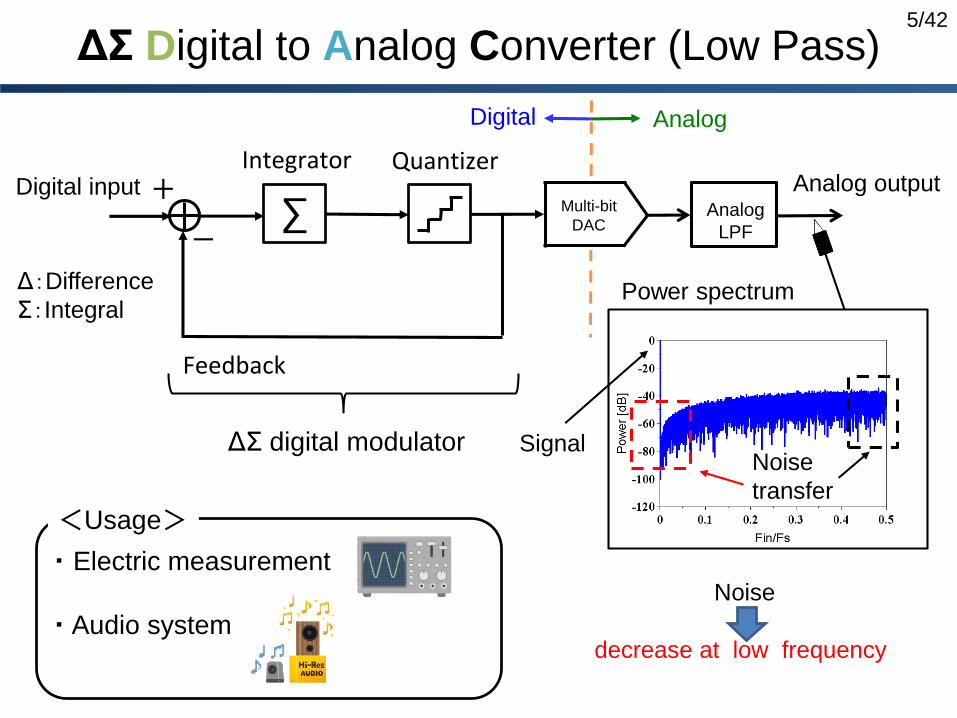
ΔΣ Digital to Analog Converter (Low Pass)
ΔΣ digital modulator
Quantizer
Feedback
Integrator+
−Analog
LPF∑ Multi-bit
DAC
Analog output
・ Electric measurement
・ Audio system
Digital input
Digital Analog
Signal
Δ:Difference
Σ:Integral
Noise
decrease at low frequency
Noise
transfer
<Usage>
Power spectrum
6/42
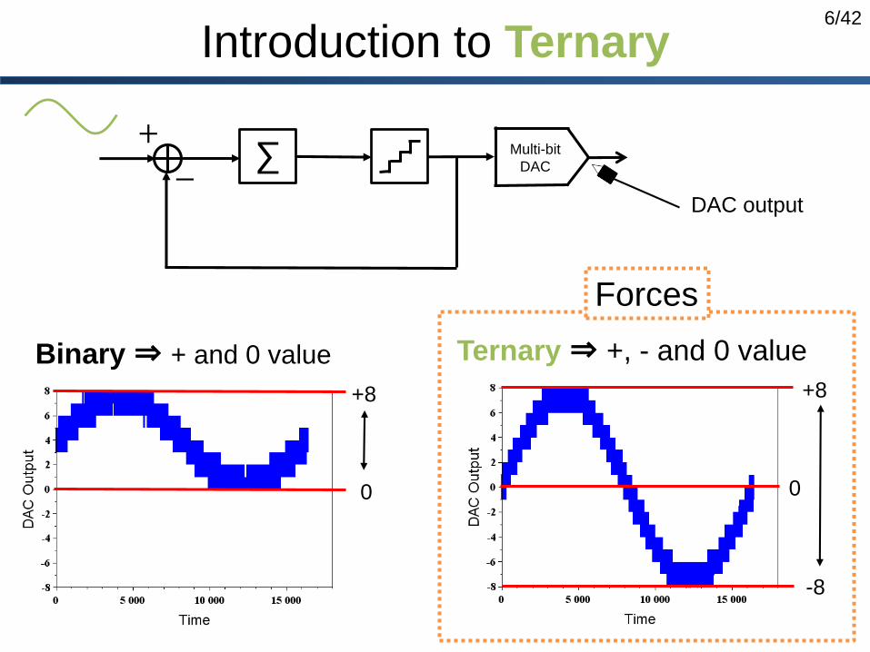
Introduction to Ternary
+
−∑ Multi-bit
DAC
+8
0 0
+8
-8
DAC output
Ternary⇒ +, - and 0 valueBinary ⇒ + and 0 value
Forces
7/42
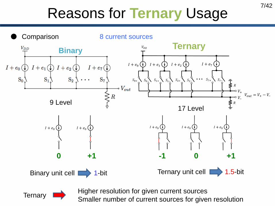
Reasons for Ternary Usage
Ternary
9 Level17 Level
Binary
8 current sources● Comparison
0 +1 +10-1
Binary unit cell 1-bit Ternary unit cell 1.5-bit
Higher resolution for given current sources
Smaller number of current sources for given resolutionTernary
8/42
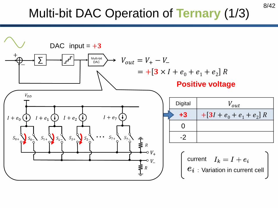
Multi-bit DAC Operation of Ternary (1/3)
Digital 𝑉𝑜𝑢𝑡
+3 + 𝟑𝐼 + 𝑒0+ 𝑒1+ 𝑒2 𝑅
0
-2
: Variation in current cell
current
DAC input = +𝟑
𝑉𝑜𝑢𝑡 = 𝑉+ − 𝑉−
Positive voltage
= + 𝟑 × 𝐼 + 𝑒0+ 𝑒1+ 𝑒2 𝑅
9/42
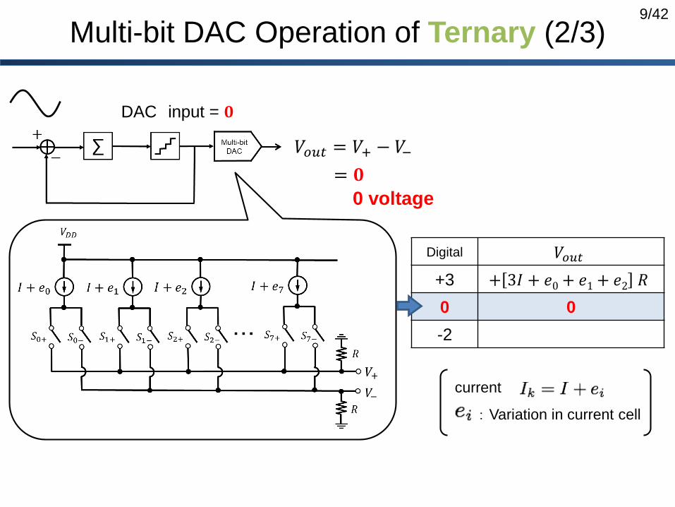
Multi-bit DAC Operation of Ternary (2/3)
Digital 𝑉𝑜𝑢𝑡
+3 + 3𝐼 + 𝑒0+ 𝑒1+ 𝑒2 𝑅
0 0
-2
: Variation in current cell
current
DAC input = 𝟎
𝑉𝑜𝑢𝑡 = 𝑉+ − 𝑉−
0 voltage
= 𝟎
10/42
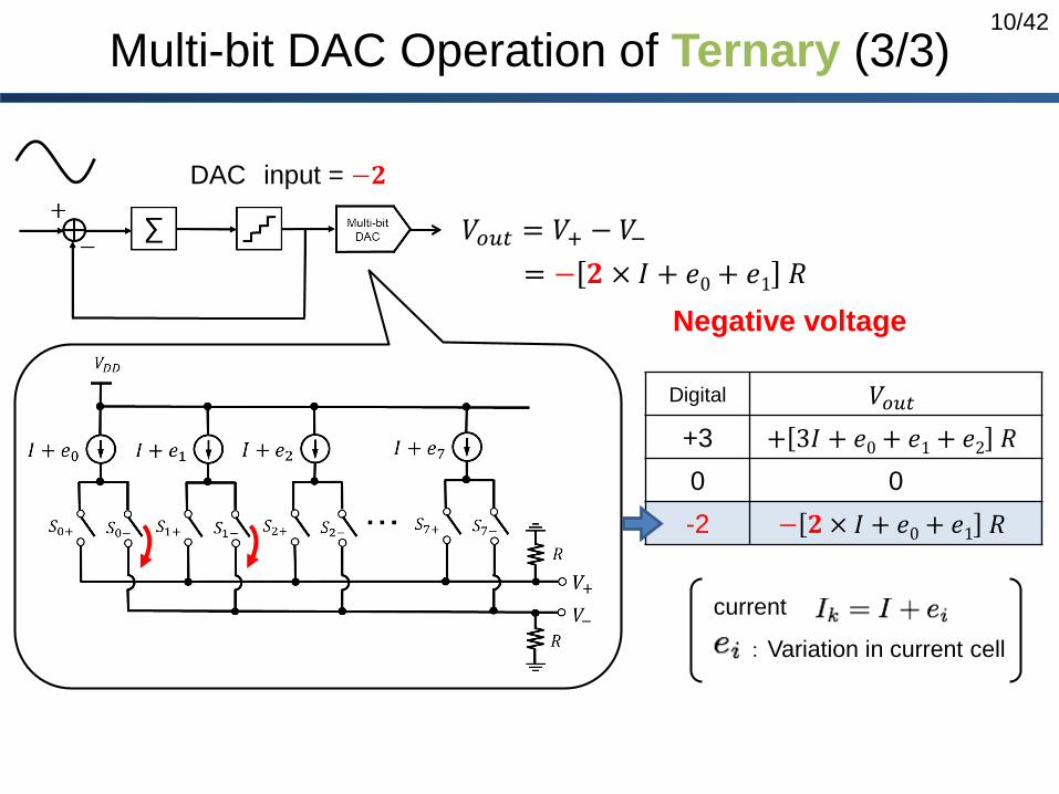
Multi-bit DAC Operation of Ternary (3/3)
Digital 𝑉𝑜𝑢𝑡
+3 + 3𝐼 + 𝑒0+ 𝑒1+ 𝑒2 𝑅
0 0
-2 − 𝟐 × 𝐼 + 𝑒0+ 𝑒1 𝑅
: Variation in current cell
current
DAC input = −𝟐
𝑉𝑜𝑢𝑡 = 𝑉+ − 𝑉−
Negative voltage
= − 𝟐 × 𝐼 + 𝑒0+ 𝑒1 𝑅
11/42
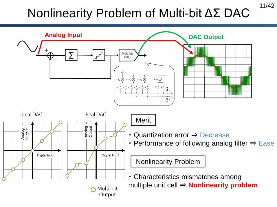
Nonlinearity Problem of Multi-bit ΔΣ DAC
DAC OutputAnalog Input
・ Quantization error ⇒ Decrease
・ Performance of following analog filter ⇒ Ease
Merit
Nonlinearity Problem
・ Characteristics mismatches among
multiple unit cell⇒ Nonlinearity problem
12/42
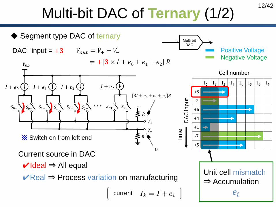
Multi-bit DAC of Ternary (1/2)
current
DAC input = +𝟑 𝑉𝑜𝑢𝑡 = 𝑉+ − 𝑉−
= + 𝟑 × 𝐼 + 𝑒0+ 𝑒1+ 𝑒2 𝑅
Positive Voltage
Negative Voltage
0
3𝐼 + 𝑒0+ 𝑒1+ 𝑒2 𝑅
※ Switch on from left end
◆ Segment type DAC of ternary
Unit cell mismatch
⇒ Accumulation
𝑒𝑖
Current source in DAC
✔Ideal ⇒ All equal
✔Real ⇒ Process variation on manufacturing
13/42
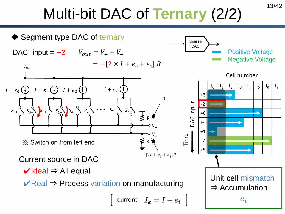
Multi-bit DAC of Ternary (2/2)
current
DAC input = −𝟐 𝑉𝑜𝑢𝑡 = 𝑉+ − 𝑉−
= − 2 × 𝐼 + 𝑒0+ 𝑒1 𝑅
Positive Voltage
Negative Voltage
0
※ Switch on from left end
◆ Segment type DAC of ternary
Unit cell mismatch
⇒ Accumulation
𝑒𝑖
Current source in DAC
✔Ideal ⇒ All equal
2𝐼 + 𝑒0+ 𝑒1 𝑅
✔Real ⇒ Process variation on manufacturing
14/42
Outline
Research Background
ΔΣDA Converter
DWA*Algorithm (* Data-Weighted Averaging)
Simulation Verification
Binary, Ternary DWA Overview
ΔΣ DA Converter : HP type
ΔΣ DA Converter : BP type
Conclusion
15/42
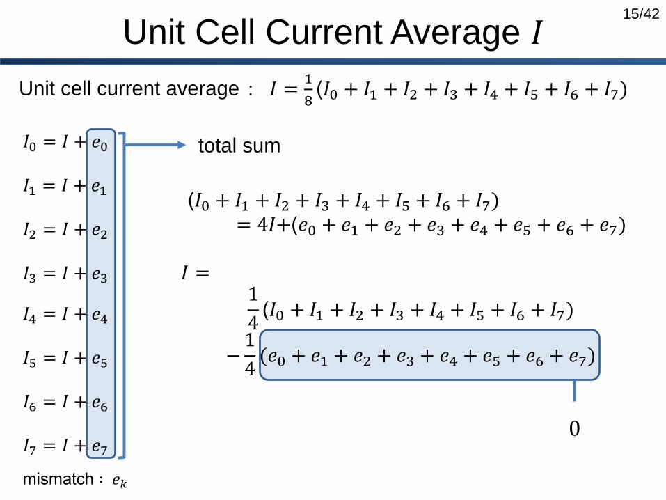
Unit Cell Current Average 𝐼
Unit cell current average : 𝐼 =1
8(𝐼0 + 𝐼1 + 𝐼2 + 𝐼3 + 𝐼4 + 𝐼5 + 𝐼6 + 𝐼7)
𝐼0 = 𝐼 + 𝑒0
𝐼1 = 𝐼 + 𝑒1
𝐼2 = 𝐼 + 𝑒2
𝐼3 = 𝐼 + 𝑒3
total sum
𝐼 =1
4(𝐼0 + 𝐼1 + 𝐼2 + 𝐼3 + 𝐼4 + 𝐼5 + 𝐼6 + 𝐼7)
−1
4(𝑒0 + 𝑒1 + 𝑒2 + 𝑒3 + 𝑒4 + 𝑒5 + 𝑒6 + 𝑒7)
(𝐼0 + 𝐼1 + 𝐼2 + 𝐼3 + 𝐼4 + 𝐼5 + 𝐼6 + 𝐼7)= 4𝐼+(𝑒0 + 𝑒1 + 𝑒2 + 𝑒3 + 𝑒4 + 𝑒5 + 𝑒6 + 𝑒7)
0
mismatch ∶ 𝑒𝑘
𝐼4 = 𝐼 + 𝑒4
𝐼5 = 𝐼 + 𝑒5
𝐼6 = 𝐼 + 𝑒6
𝐼7 = 𝐼 + 𝑒7
16/42
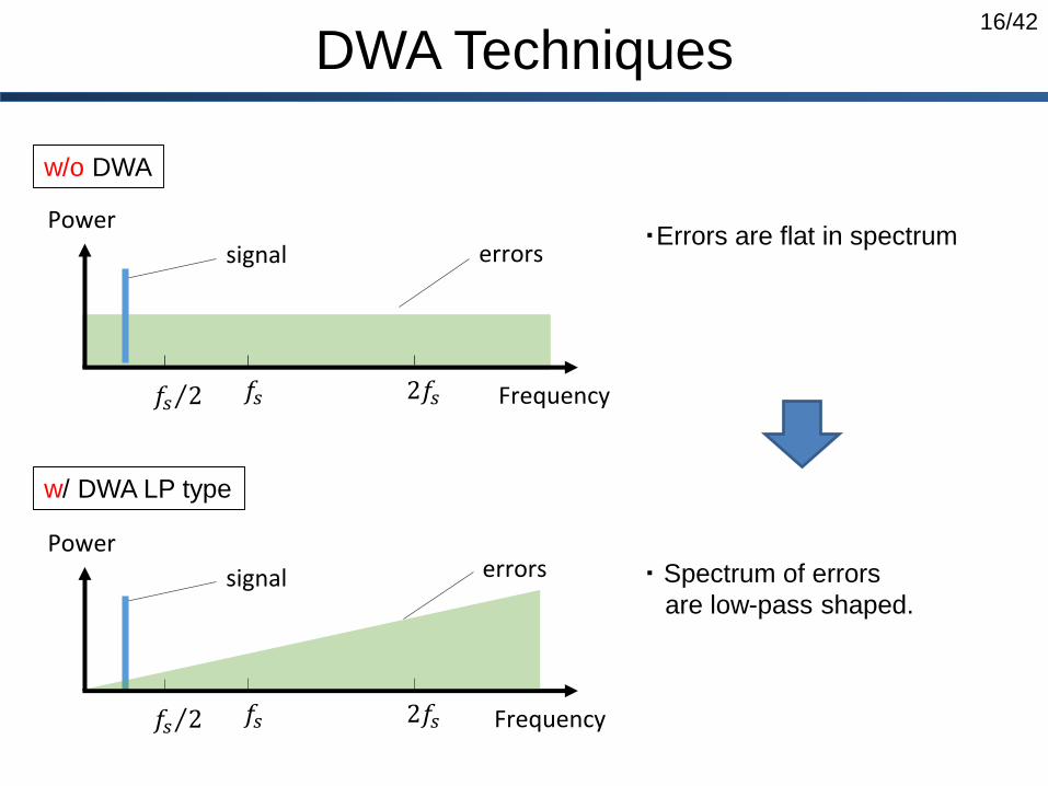
DWA Techniques
Τ𝑓𝑠 2 𝑓𝑠
Power
signal errors
2𝑓𝑠 Frequency
Τ𝑓𝑠 2 𝑓𝑠
Power
signal errors
2𝑓𝑠 Frequency
w/o DWA
w/ DWA LP type
・ Spectrum of errors
are low-pass shaped.
・Errors are flat in spectrum
17/42
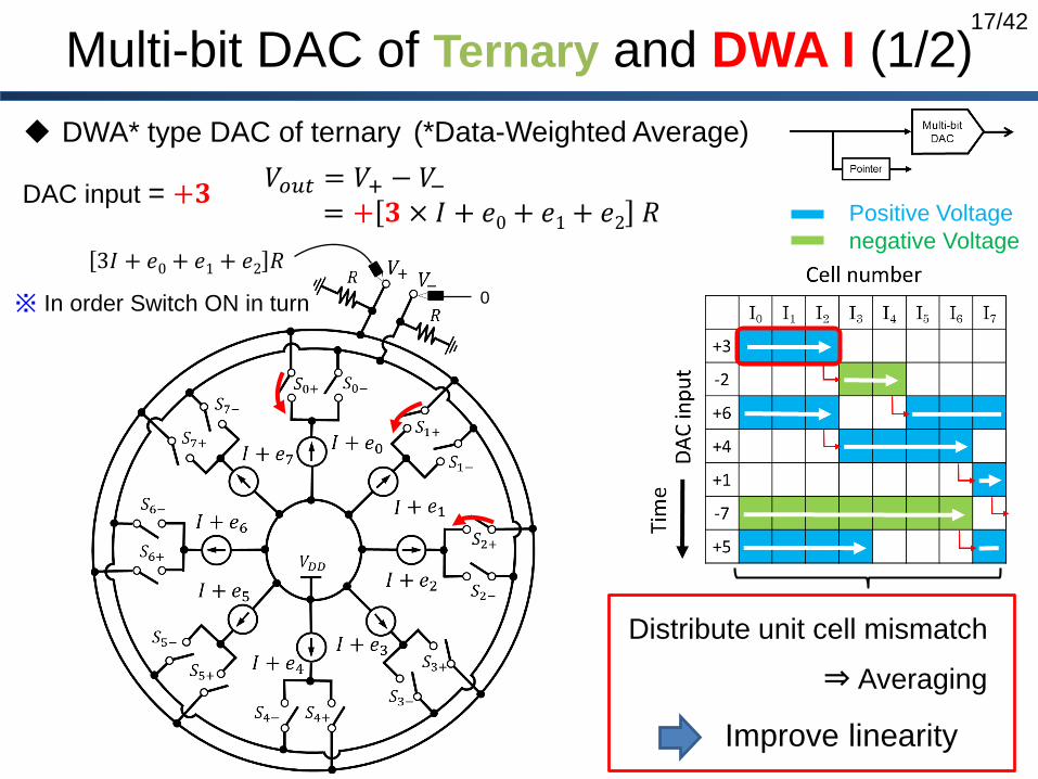
Multi-bit DAC of Ternary and DWA I (1/2)
(*Data-Weighted Average)
※ In order Switch ON in turn
DAC input = +𝟑
DWA* type DAC of ternary
𝑉𝑜𝑢𝑡 = 𝑉+ − 𝑉−= + 𝟑 × 𝐼 + 𝑒0+ 𝑒1+ 𝑒2 𝑅
Improve linearity
⇒ Averaging
0
3𝐼 + 𝑒0 + 𝑒1 + 𝑒2 𝑅
Positive Voltage
negative Voltage
Distribute unit cell mismatch
18/42
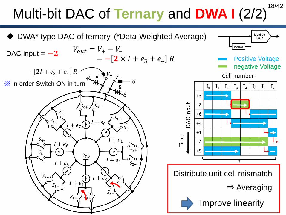
Multi-bit DAC of Ternary and DWA I (2/2)
(*Data-Weighted Average)
※ In order Switch ON in turn
DAC input = −𝟐
DWA* type DAC of ternary
𝑉𝑜𝑢𝑡 = 𝑉+ − 𝑉−= − 𝟐 × 𝐼 + 𝑒3 + 𝑒4 𝑅
Improve linearity
⇒ Averaging
0
Positive Voltage
negative Voltage
Distribute unit cell mismatch
− 𝟐𝐼 + 𝑒3 + 𝑒4 𝑅
19/42
Multi-bit DAC of Ternary and DWA II (1/3)
(*Data-Weighted Average)
※ In order Switch ON in turn
DAC input = +𝟑
DWA* type DAC of ternary
𝑉𝑜𝑢𝑡 = 𝑉+ − 𝑉−= + 𝟑 × 𝐼 + 𝑒0+ 𝑒1+ 𝑒2 𝑅
Improve linearity
⇒ Averaging
0
3𝐼 + 𝑒0+ 𝑒1 + 𝑒2 𝑅
Positive Voltage
negative Voltage
Distribute unit cell mismatch
Back and forth
20/42
Multi-bit DAC of Ternary and DWA II (2/3)
(*Data-Weighted Average)
※ In order Switch ON in turn
DAC input = −𝟐
DWA* type DAC of ternary
𝑉𝑜𝑢𝑡 = 𝑉+ − 𝑉−= − 𝟐 × 𝐼 + 𝑒1+ 𝑒2 𝑅
Improve linearity
⇒ Averaging
0
Positive Voltage
negative Voltage
Distribute unit cell mismatch
− 𝟐𝐼 + 𝑒1 + 𝑒2 𝑅
Back and forth
21/42
Multi-bit DAC of Ternary and DWA II (3/3)
(*Data-Weighted Average)
※ In order Switch ON in turn
DAC input = +𝟔
DWA* type DAC of ternary
𝑉𝑜𝑢𝑡 = 𝑉+ − 𝑉−= + 𝟔 × 𝐼 + 𝑒1 +⋯+ 𝑒6 𝑅
Improve linearity
⇒ Averaging
0
Positive Voltage
negative Voltage
Distribute unit cell mismatch
𝟔𝐼 + 𝑒1 +⋯+ 𝑒6 𝑅
Back and forth
22/42
DWA type I (Pointer)
I0 I1 I2 I3 I4 I5 I6 I7
+3
-2
+6
+4
+1
-7
+5
I0 I1 I2 I3 I4 I5 I6 I7
+3
-2
+6
+4
+1
-7
+5
1 Pointer 2 Pointers
23/42
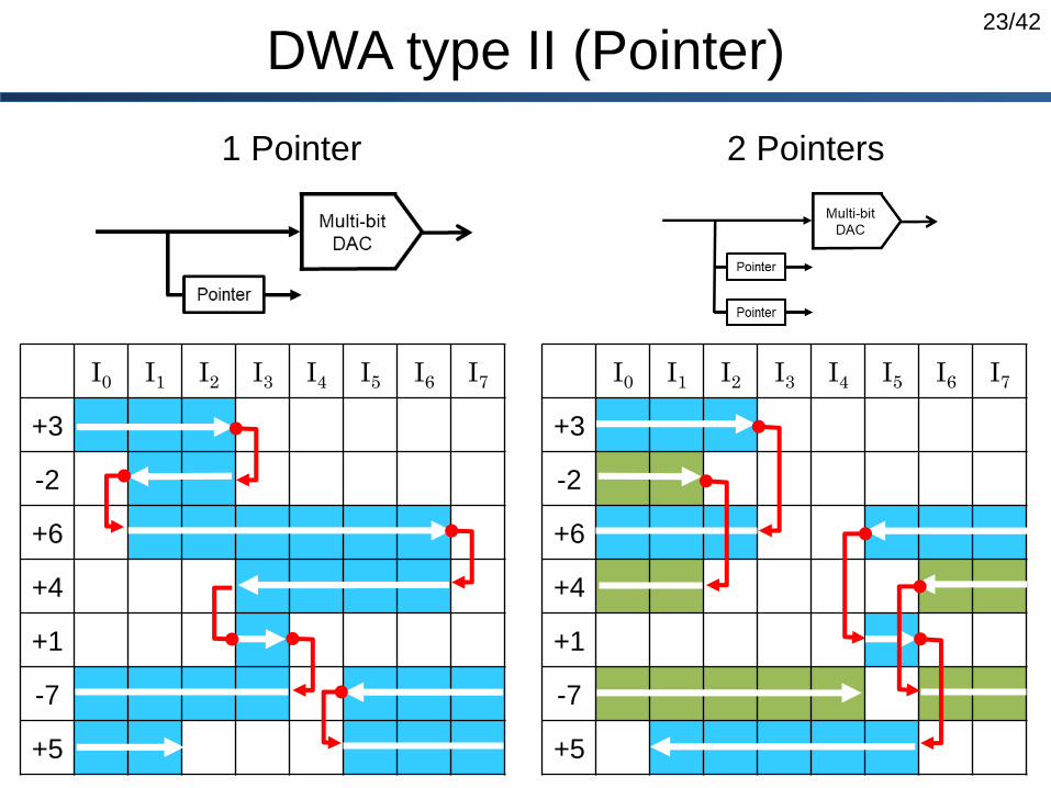
DWA type II (Pointer)
I0 I1 I2 I3 I4 I5 I6 I7
+3
-2
+6
+4
+1
-7
+5
I0 I1 I2 I3 I4 I5 I6 I7
+3
-2
+6
+4
+1
-7
+5
1 Pointer 2 Pointers
24/42
Outline
Research Background
ΔΣDA Converter
DWA*Algorithm (* Data-Weighted Averaging)
Simulation verification
Binary, Ternary DWA Overview
ΔΣ DA Converter : HP type
ΔΣ DA Converter : BP type
Conclusion
25/42
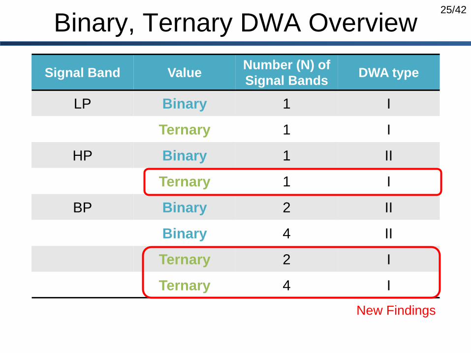
Binary, Ternary DWA Overview
Signal Band ValueNumber (N) of
Signal BandsDWA type
LP Binary 1 I
Ternary 1 I
HP Binary 1 II
Ternary 1 I
BP Binary 2 II
Binary 4 II
Ternary 2 I
Ternary 4 I
New Findings
26/42
Outline
Research Background
ΔΣDA Converter
DWA*Algorithm (* Data-Weighted Averaging)
Simulation verification
Binary, Ternary DWA Overview
ΔΣ DA Converter : HP type
ΔΣ DA Converter : BP type
Conclusion
27/42
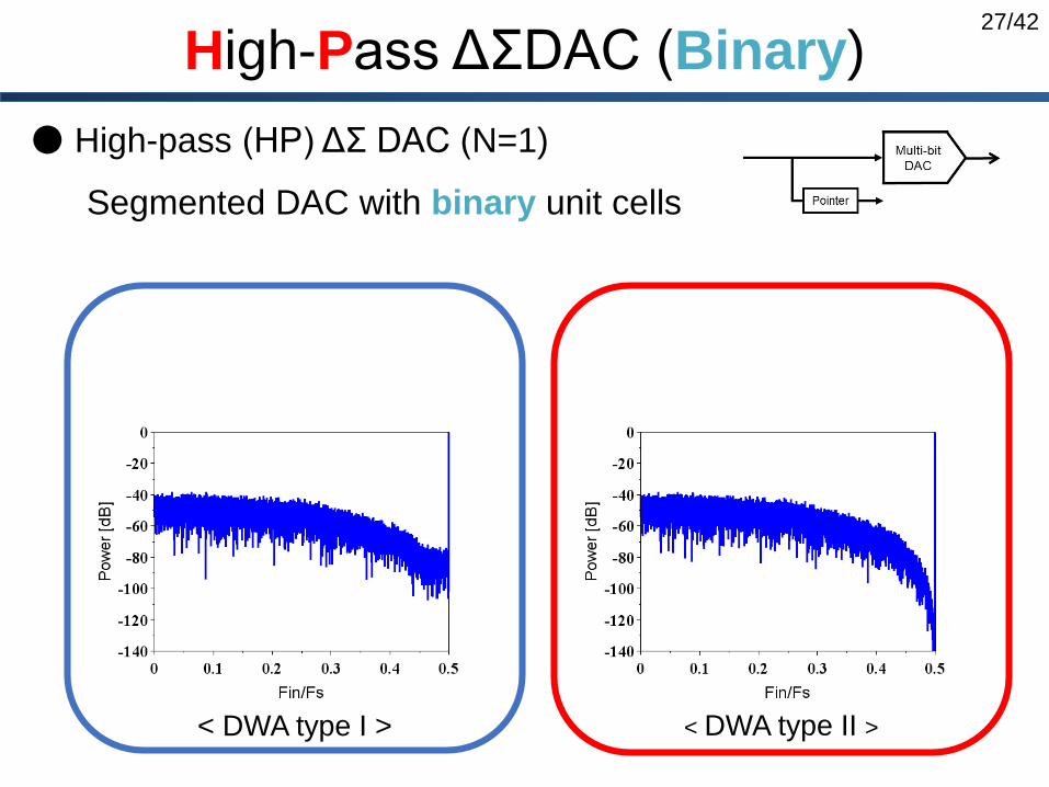
High-Pass ΔΣDAC (Binary)
● High-pass (HP) ΔΣ DAC (N=1)
Segmented DAC with binary unit cells
< DWA type II >< DWA type I >
28/42
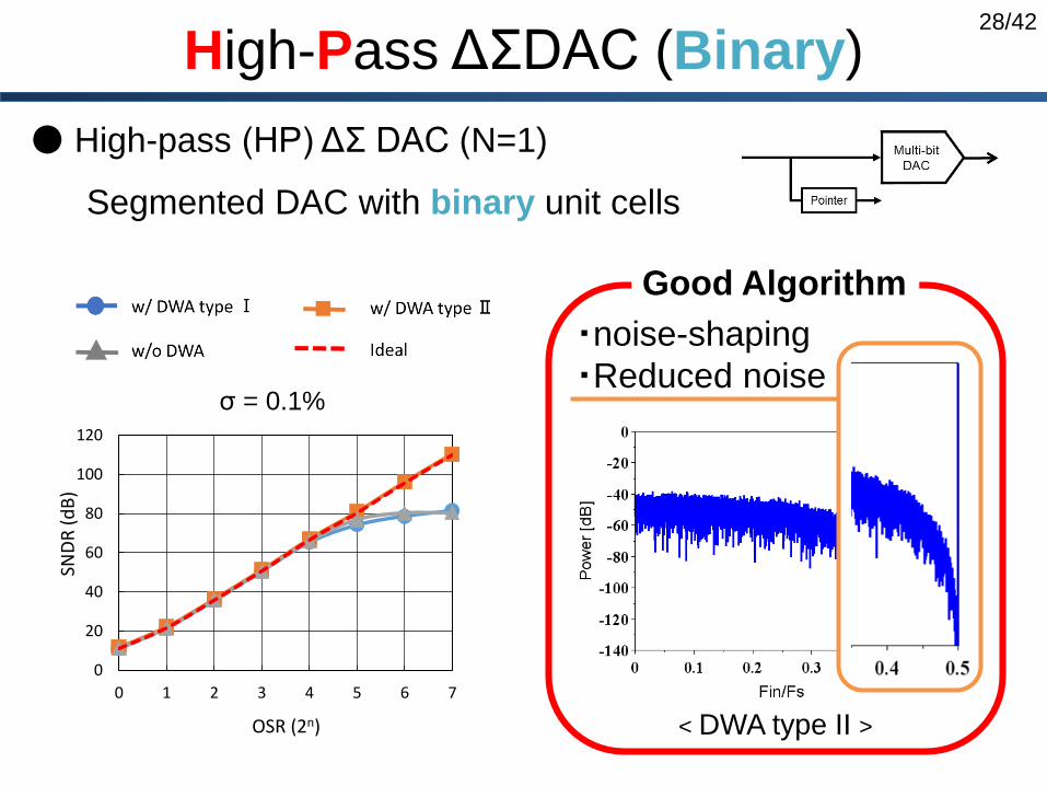
High-Pass ΔΣDAC (Binary)
● High-pass (HP) ΔΣ DAC (N=1)
Segmented DAC with binary unit cells
< DWA type II >
Good Algorithm
・noise-shaping
・Reduced noise
0
20
40
60
80
100
120
0 1 2 3 4 5 6 7
SND
R (
dB
)
OSR (2n)
σ = 0.1%
29/42
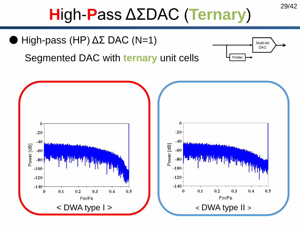
High-Pass ΔΣDAC (Ternary)
● High-pass (HP) ΔΣ DAC (N=1)
Segmented DAC with ternary unit cells
< DWA type II >< DWA type I >
30/42
0
20
40
60
80
100
120
0 1 2 3 4 5 6 7
SND
R (
dB
)
OSR (2n)
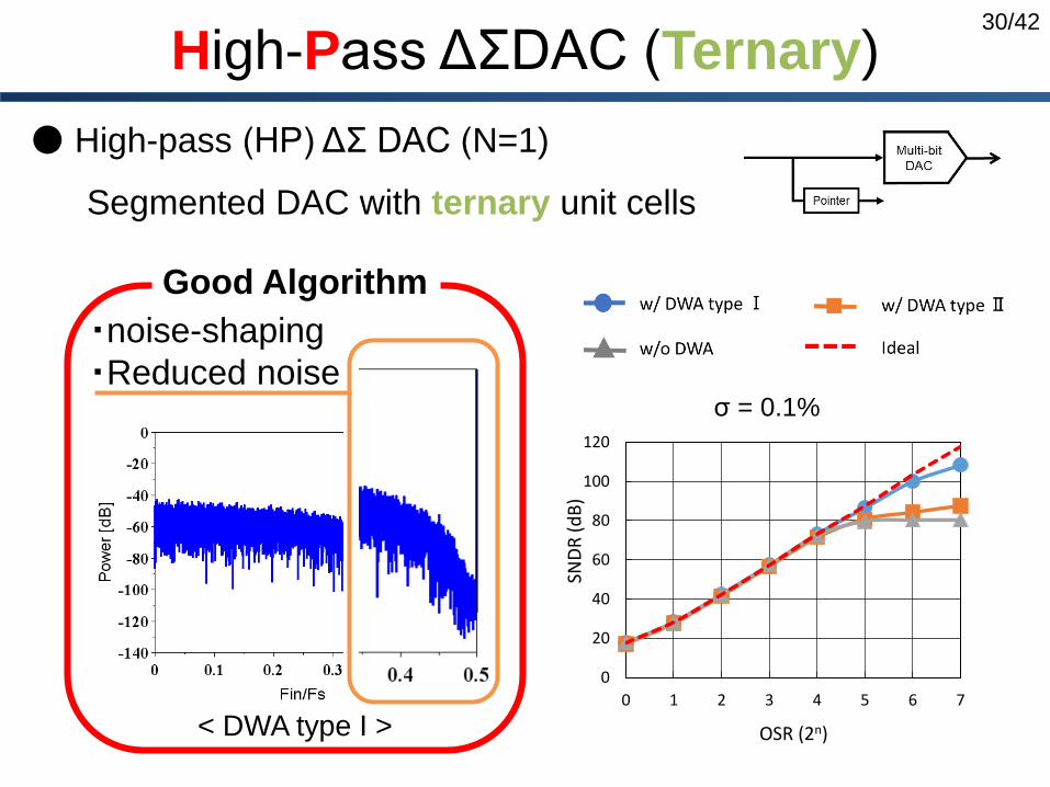
High-Pass ΔΣDAC (Ternary)
● High-pass (HP) ΔΣ DAC (N=1)
Segmented DAC with ternary unit cells
< DWA type I >
・noise-shaping
・Reduced noise
Good Algorithm
σ = 0.1%
31/42
Outline
Research Background
ΔΣDA Converter
DWA*Algorithm (* Data-Weighted Averaging)
Simulation verification
Binary, Ternary DWA Overview
ΔΣ DA Converter : HP type
ΔΣ DA Converter : BP type
Conclusion
32/42
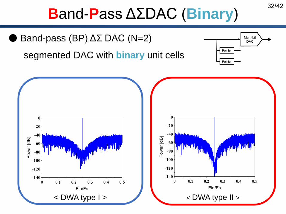
Band-Pass ΔΣDAC (Binary)
● Band-pass (BP) ΔΣ DAC (N=2)
segmented DAC with binary unit cells
< DWA type II >< DWA type I >
33/42
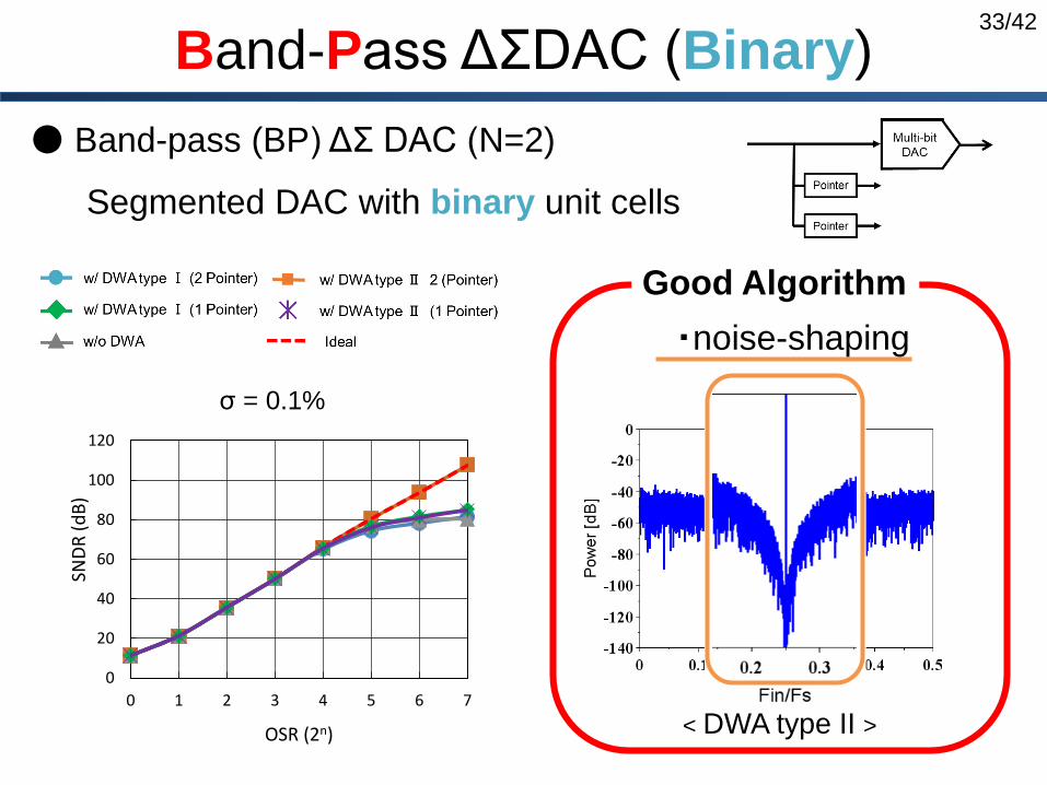
Band-Pass ΔΣDAC (Binary)
● Band-pass (BP) ΔΣ DAC (N=2)
Segmented DAC with binary unit cells
< DWA type II >
Good Algorithm
・noise-shaping
σ = 0.1%
0
20
40
60
80
100
120
0 1 2 3 4 5 6 7
SND
R (
dB
)
OSR (2n)
34/42
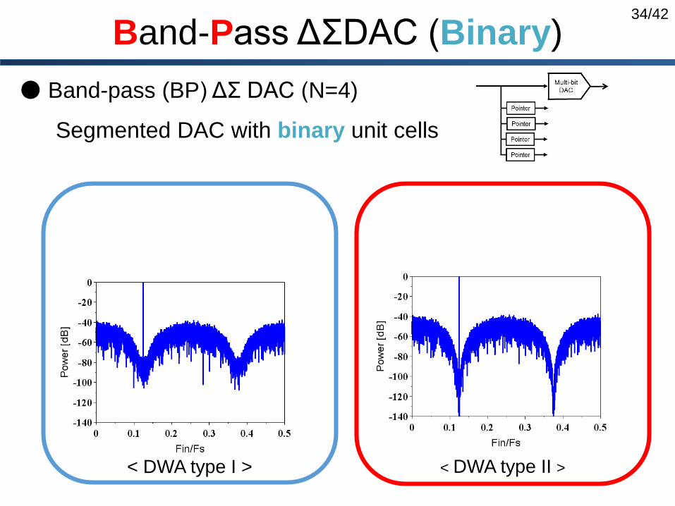
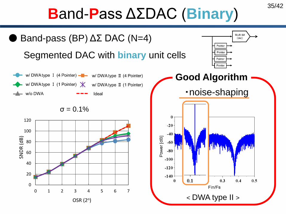
Band-Pass ΔΣDAC (Binary)
● Band-pass (BP) ΔΣ DAC (N=4)
Segmented DAC with binary unit cells
< DWA type II >< DWA type I >
35/42
0
20
40
60
80
100
120
0 1 2 3 4 5 6 7
SND
R (
dB
)
OSR (2n)
Band-Pass ΔΣDAC (Binary)
● Band-pass (BP) ΔΣ DAC (N=4)
Segmented DAC with binary unit cells
< DWA type II >
Good Algorithm
・noise-shaping
σ = 0.1%
36/42
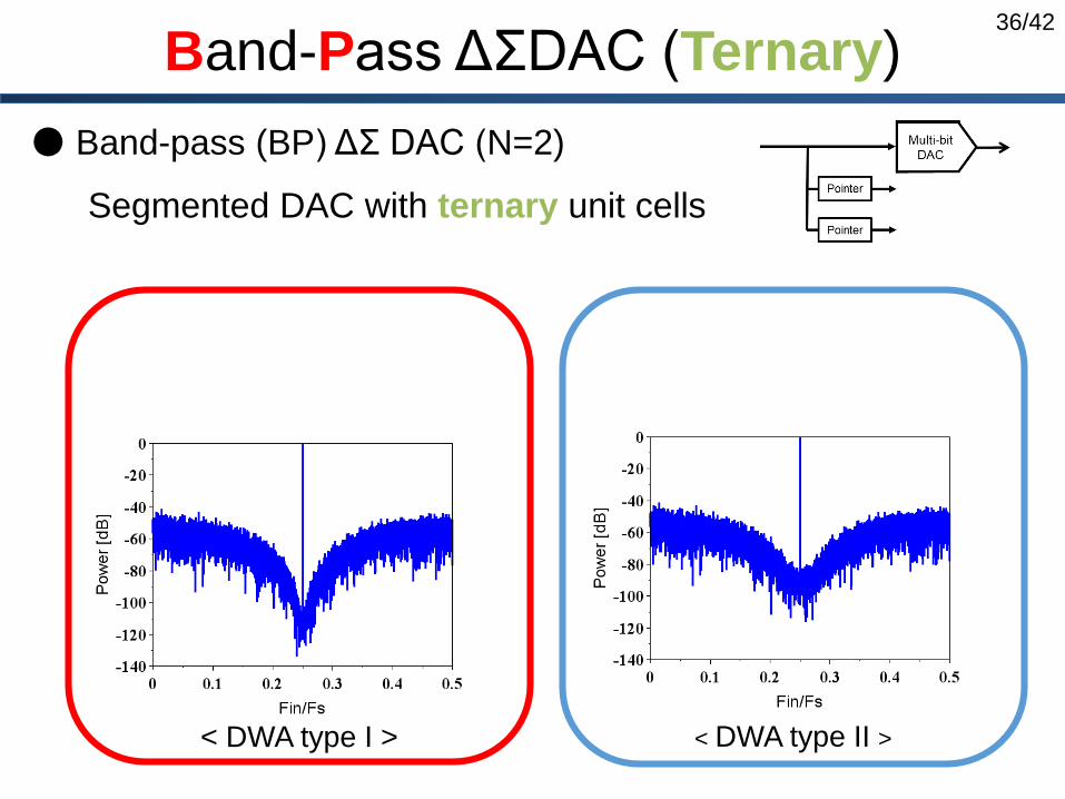
Band-Pass ΔΣDAC (Ternary)
● Band-pass (BP) ΔΣ DAC (N=2)
Segmented DAC with ternary unit cells
< DWA type II >< DWA type I >
37/42
0
20
40
60
80
100
120
0 1 2 3 4 5 6 7
SND
R (
dB
)
OSR (2n)
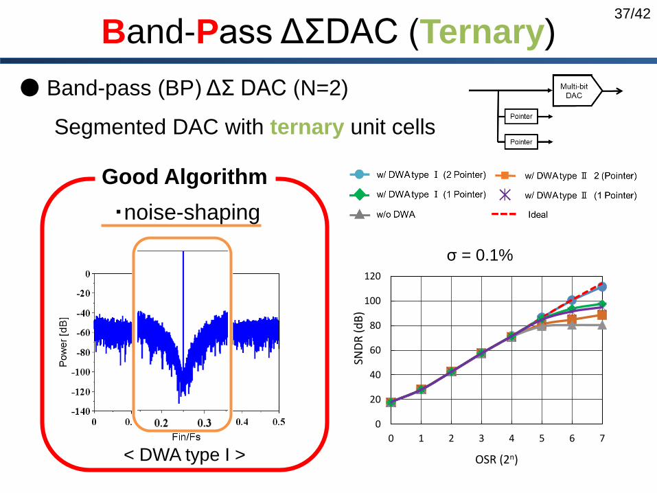
Band-Pass ΔΣDAC (Ternary)
● Band-pass (BP) ΔΣ DAC (N=2)
Segmented DAC with ternary unit cells
< DWA type I >
Good Algorithm
・noise-shaping
σ = 0.1%
38/42
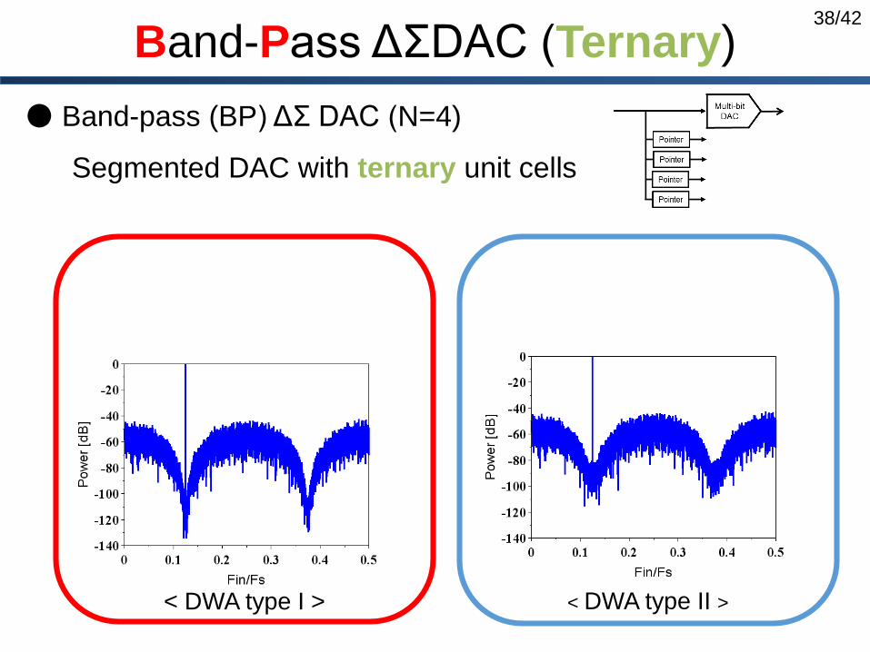
Band-Pass ΔΣDAC (Ternary)
● Band-pass (BP) ΔΣ DAC (N=4)
Segmented DAC with ternary unit cells
< DWA type II >< DWA type I >
39/42
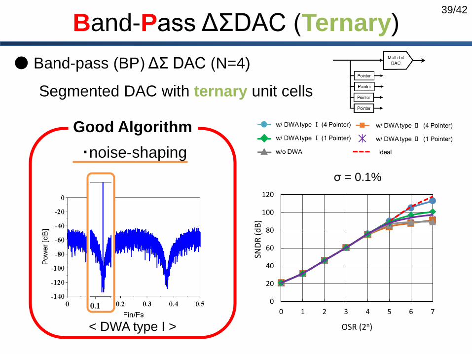
Band-Pass ΔΣDAC (Ternary)
● Band-pass (BP) ΔΣ DAC (N=4)
Segmented DAC with ternary unit cells
< DWA type I >
Good Algorithm
・noise-shaping
σ = 0.1%
0
20
40
60
80
100
120
0 1 2 3 4 5 6 7
SND
R (
dB
)
OSR (2n)
40/42
Outline
Research Background
ΔΣDA Converter
DWA*Algorithm (* Data-Weighted Averaging)
Simulation verification
Binary, Ternary DWA Overview
ΔΣ DA Converter : HP type
ΔΣ DA Converter : BP type
Conclusion
41/42
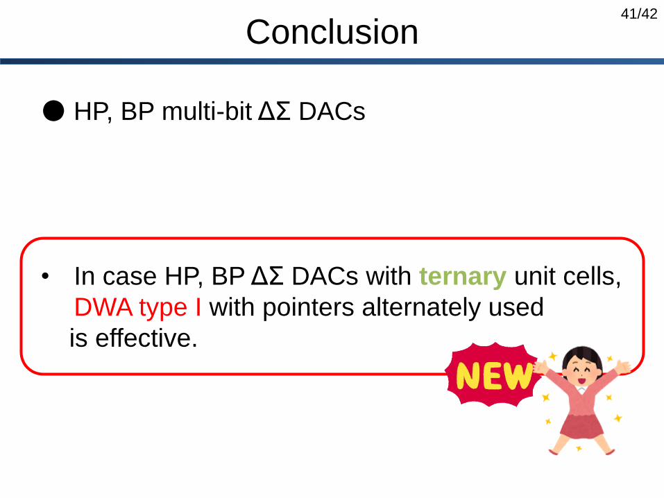
Conclusion
● HP, BP multi-bit ΔΣ DACs
• In case HP, BP ΔΣ DACs with ternary unit cells,
DWA type I with pointers alternately used
is effective.

42/42
Thank you for attention
43/42
Appendix
App.
44/42
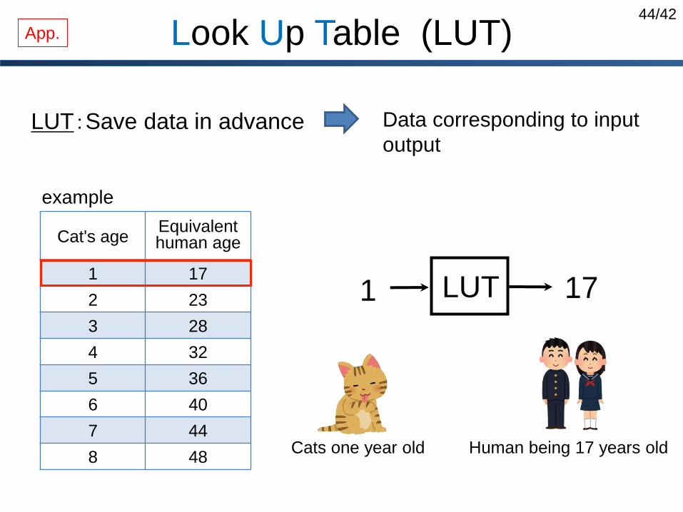
Look Up Table (LUT)
LUT:Save data in advance
Cat's ageEquivalent human age
1 17
2 23
3 28
4 32
5 36
6 40
7 44
8 48
LUT
example
171
Data corresponding to input
output
Cats one year old Human being 17 years old
App.
45/42
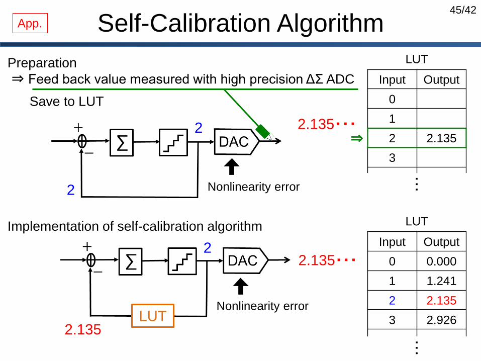
Self-Calibration Algorithm
2.135・・・
Nonlinearity error
22.135・・・
2.135LUT
Preparation
⇒ Feed back value measured with high precision ΔΣ ADC
Save to LUT
Input Output
0
1
2 2.135
3
2
LUT・・・
Input Output
0 0.000
1 1.241
2 2.135
3 2.926
LUT
・・・
⇒
Nonlinearity error
2
Implementation of self-calibration algorithm
App.


![nP q arXiv:1205.5252v4 [math.NT] 30 Dec 2013 · 2013-12-31 · arXiv:1205.5252v4 [math.NT] 30 Dec 2013 MINOR ARCS FOR GOLDBACH’S PROBLEM H. A. HELFGOTT Abstract. The ternary Goldbach](https://static.fdocument.org/doc/165x107/5e68df189e8aca31703bbe63/np-q-arxiv12055252v4-mathnt-30-dec-2013-2013-12-31-arxiv12055252v4-mathnt.jpg)