Dual High-Speed Differential Line Driver (Rev. C) · PDF fileexceeding 15 Mbps in properly...
12
uA9638C DUAL HIGH-SPEED DIFFERENTIAL LINE DRIVER SLLS112C - OCTOBER 1980 - REVISED APRIL 1994 1 POST OFFICE BOX 655303 • DALLAS, TEXAS 75265 D Meets or Exceeds ANSI Standard EIA/TIA-422-B D Operates From a Single 5-V Power Supply D Drives Loads as Low as 50 Ω up to 15 Mbps D TTL- and CMOS-Input Compatibility D Output Short-Circuit Protection D Interchangeable With National Semiconductor™ DS9638 description The uA9638C is a dual high-speed differential line driver designed to meet ANSI Standard EIA / TIA-422-B. The inputs are TTL and CMOS compatible and have input clamp diodes. Schottky-diode-clamped transistors are used to minimize propagation delay time. This device operates from a single 5-V power supply and is supplied in an 8-pin package. The uA9638 provides the current needed to drive low-impedance loads at high speeds. Typically used with twisted-pair cabling and differential receiver(s), base-band data transmission can be accomplished up to and exceeding 15 Mbps in properly designed systems. The uA9637A dual line receiver is commonly used as the receiver. For even faster switching speeds in the same pin configuration, see the SN75ALS191. The uA9638C is characterized for operation from 0°C to 70°C. logic symbol † † This symbol is in accordance with ANSI/IEEE Std 91-1984 and IEC Publication 617-12. 2A 1A 5 6 7 8 2Z 2Y 1Z 1Y 3 2 logic diagram 2Z 2Y 1Z 1Y 3 2 2A 1A 5 6 7 8 Copyright © 1994, Texas Instruments Incorporated PRODUCTION DATA information is current as of publication date. Products conform to specifications per the terms of Texas Instruments standard warranty. Production processing does not necessarily include testing of all parameters. Please be aware that an important notice concerning availability, standard warranty, and use in critical applications of Texas Instruments semiconductor products and disclaimers thereto appears at the end of this data sheet. National Semiconductor is a trademark of National Semiconductor Corporation. 1 2 3 4 8 7 6 5 V CC 1A 2A GND 1Y 1Z 2Y 2Z D OR P PACKAGE (TOP VIEW)
Transcript of Dual High-Speed Differential Line Driver (Rev. C) · PDF fileexceeding 15 Mbps in properly...
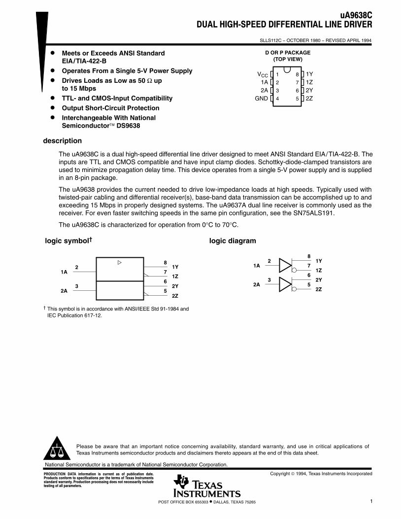
uA9638CDUAL HIGH-SPEED DIFFERENTIAL LINE DRIVER
SLLS112C − OCTOBER 1980 − REVISED APRIL 1994
1POST OFFICE BOX 655303 • DALLAS, TEXAS 75265
� Meets or Exceeds ANSI StandardEIA/TIA-422-B
� Operates From a Single 5-V Power Supply
� Drives Loads as Low as 50 Ω up to 15 Mbps
� TTL- and CMOS-Input Compatibility
� Output Short-Circuit Protection
� Interchangeable With NationalSemiconductor™ DS9638
description
The uA9638C is a dual high-speed differential line driver designed to meet ANSI Standard EIA/TIA-422-B. Theinputs are TTL and CMOS compatible and have input clamp diodes. Schottky-diode-clamped transistors areused to minimize propagation delay time. This device operates from a single 5-V power supply and is suppliedin an 8-pin package.
The uA9638 provides the current needed to drive low-impedance loads at high speeds. Typically used withtwisted-pair cabling and differential receiver(s), base-band data transmission can be accomplished up to andexceeding 15 Mbps in properly designed systems. The uA9637A dual line receiver is commonly used as thereceiver. For even faster switching speeds in the same pin configuration, see the SN75ALS191.
The uA9638C is characterized for operation from 0°C to 70°C.
logic symbol†
† This symbol is in accordance with ANSI/IEEE Std 91-1984 andIEC Publication 617-12.
2A
1A
5
6
7
8
2Z
2Y
1Z
1Y
3
2
logic diagram
2Z
2Y
1Z
1Y
3
2
2A
1A
5
6
7
8
Copyright © 1994, Texas Instruments IncorporatedPRODUCTION DATA information is current as of publication date.Products conform to specifications per the terms of Texas Instrumentsstandard warranty. Production processing does not necessarily includetesting of all parameters.
Please be aware that an important notice concerning availability, standard warranty, and use in critical applications ofTexas Instruments semiconductor products and disclaimers thereto appears at the end of this data sheet.
National Semiconductor is a trademark of National Semiconductor Corporation.
1
2
3
4
8
7
6
5
VCC
1A2A
GND
1Y1Z2Y2Z
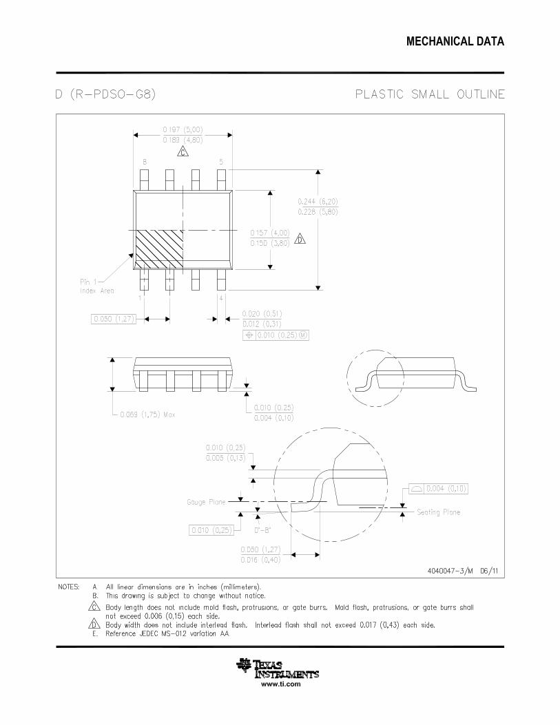
D OR P PACKAGE(TOP VIEW)
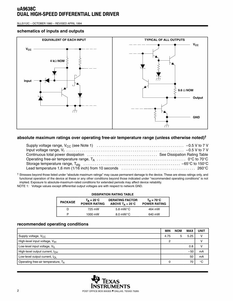
uA9638CDUAL HIGH-SPEED DIFFERENTIAL LINE DRIVER
SLLS112C − OCTOBER 1980 − REVISED APRIL 1994
2 POST OFFICE BOX 655303 • DALLAS, TEXAS 75265
schematics of inputs and outputs
VCC
EQUIVALENT OF EACH INPUT TYPICAL OF ALL OUTPUTS
Input
4 kΩ NOM
VCC
Output
GND
9.6 Ω NOM
absolute maximum ratings over operating free-air temperature range (unless otherwise noted)†
Supply voltage range, VCC (see Note 1) −0.5 V to 7 V. . . . . . . . . . . . . . . . . . . . . . . . . . . . . . . . . . . . . . . . . . . . . . Input voltage range, VI −0.5 V to 7 V. . . . . . . . . . . . . . . . . . . . . . . . . . . . . . . . . . . . . . . . . . . . . . . . . . . . . . . . . . . . . . Continuous total power dissipation See Dissipation Rating Table. . . . . . . . . . . . . . . . . . . . . . . . . . . . . . . . . . . . . Operating free-air temperature range, TA 0°C to 70°C. . . . . . . . . . . . . . . . . . . . . . . . . . . . . . . . . . . . . . . . . . . . . . . Storage temperature range, Tstg −65°C to 150°C. . . . . . . . . . . . . . . . . . . . . . . . . . . . . . . . . . . . . . . . . . . . . . . . . . . Lead temperature 1,6 mm (1/16 inch) from 10 seconds 260°C. . . . . . . . . . . . . . . . . . . . . . . . . . . . . . . . . . . . . . .
† Stresses beyond those listed under “absolute maximum ratings” may cause permanent damage to the device. These are stress ratings only, andfunctional operation of the device at these or any other conditions beyond those indicated under “recommended operating conditions” is notimplied. Exposure to absolute-maximum-rated conditions for extended periods may affect device reliability.
NOTE 1: Voltage values except differential output voltages are with respect to network GND.
DISSIPATION RATING TABLE
PACKAGETA = 25°C DERATING FACTOR TA = 70°C
PACKAGETA = 25 C
POWER RATINGDERATING FACTOR
ABOVE TA = 25°CTA = 70 C
POWER RATING
D 725 mW 5.8 mW/°C 464 mW
P 1000 mW 8.0 mW/°C 640 mW
recommended operating conditions
MIN NOM MAX UNIT
Supply voltage, VCC 4.75 5 5.25 V
High-level input voltage, VIH 2 V
Low-level input voltage, VIL 0.8 V
High-level output current, IOH −50 mA
Low-level output current, IOL 50 mA
Operating free-air temperature, TA 0 70 °C
uA9638CDUAL HIGH-SPEED DIFFERENTIAL LINE DRIVER
SLLS112C − OCTOBER 1980 − REVISED APRIL 1994
3POST OFFICE BOX 655303 • DALLAS, TEXAS 75265
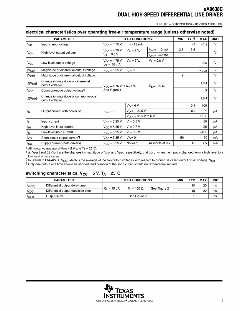
electrical characteristics over operating free-air temperature range (unless otherwise noted)
PARAMETER TEST CONDITIONS MIN TYP† MAX UNIT
VIK Input clamp voltage VCC = 4.75 V, II = −18 mA −1 −1.2 V
V High level output voltageVCC = 4.75 V, VIH = 2 V, IOH = −10 mA 2.5 3.5
VVOH High-level output voltageVCC = 4.75 V,VIL = 0.8 V
VIH = 2 V,
IOH = −40 mA 2V
V Low level output voltageVCC = 4.75 V, VIH = 2 V, VIL = 0.8 V,
0 5 VVOL Low-level output voltageVCC = 4.75 V,IOL = 40 mA
VIH = 2 V, VIL = 0.8 V, 0.5 V
|VOD1| Magnitude of differential output voltage VCC = 5.25 V, IO = 0 2VOD2 V
|VOD2| Magnitude of differential output voltage 2 V
Δ|V |Change in magnitude of differential ±0 4 VΔ|VOD|Change in magnitude of differentialoutput voltage‡ VCC = 4.75 V to 5.25 V, RL = 100 Ω,
±0.4 V
VOC Common-mode output voltage§VCC = 4.75 V to 5.25 V,See Figure 1
RL = 100 Ω, 3 V
Δ|V |Change in magnitude of common-mode ±0 4 VΔ|VOC|Change in magnitude of common-modeoutput voltage‡ ±0.4 V
VO = 6 V 0.1 100
IO Output current with power off VCC = 0 VO = − 0.25 V −0.1 −100 μAIO Output current with power off VCC 0
VO = − 0.25 V to 6 V ±100
μA
II Input current VCC = 5.25 V, VI = 5.5 V 50 μA
IIH High-level input current VCC = 5.25 V, VI = 2.7 V 25 μA
IIL Low-level input current VCC = 5.25 V, VI = 0.5 V −200 μA
IOS Short-circuit output current¶ VCC = 5.25 V, VO = 0 −50 −150 mA
ICC Supply current (both drivers) VCC = 5.25 V, No load, All inputs at 0 V 45 65 mA† All typical values are at VCC = 5 V and TA = 25°C.‡ Δ | VOD | and Δ | VOC | are the changes in magnitude of VOD and VOC, respectively, that occur when the input is changed from a high level to a
low level or vice versa.§ In Standard EIA-422-A, VOC, which is the average of the two output voltages with respect to ground, is called output offset voltage, VOS.¶ Only one output at a time should be shorted, and duration of the short circuit should not exceed one second.
switching characteristics, VCC = 5 V, TA = 25°CPARAMETER TEST CONDITIONS MIN TYP MAX UNIT
td(OD) Differential output delay timeC 15 pF R 100 Ω See Figure 2
10 20 ns
tt(OD) Differential output transition timeCL = 15 pF, RL = 100 Ω, See Figure 2
10 20 ns
tsk(o) Output skew See Figure 2 1 ns
uA9638CDUAL HIGH-SPEED DIFFERENTIAL LINE DRIVER
SLLS112C − OCTOBER 1980 − REVISED APRIL 1994
4 POST OFFICE BOX 655303 • DALLAS, TEXAS 75265
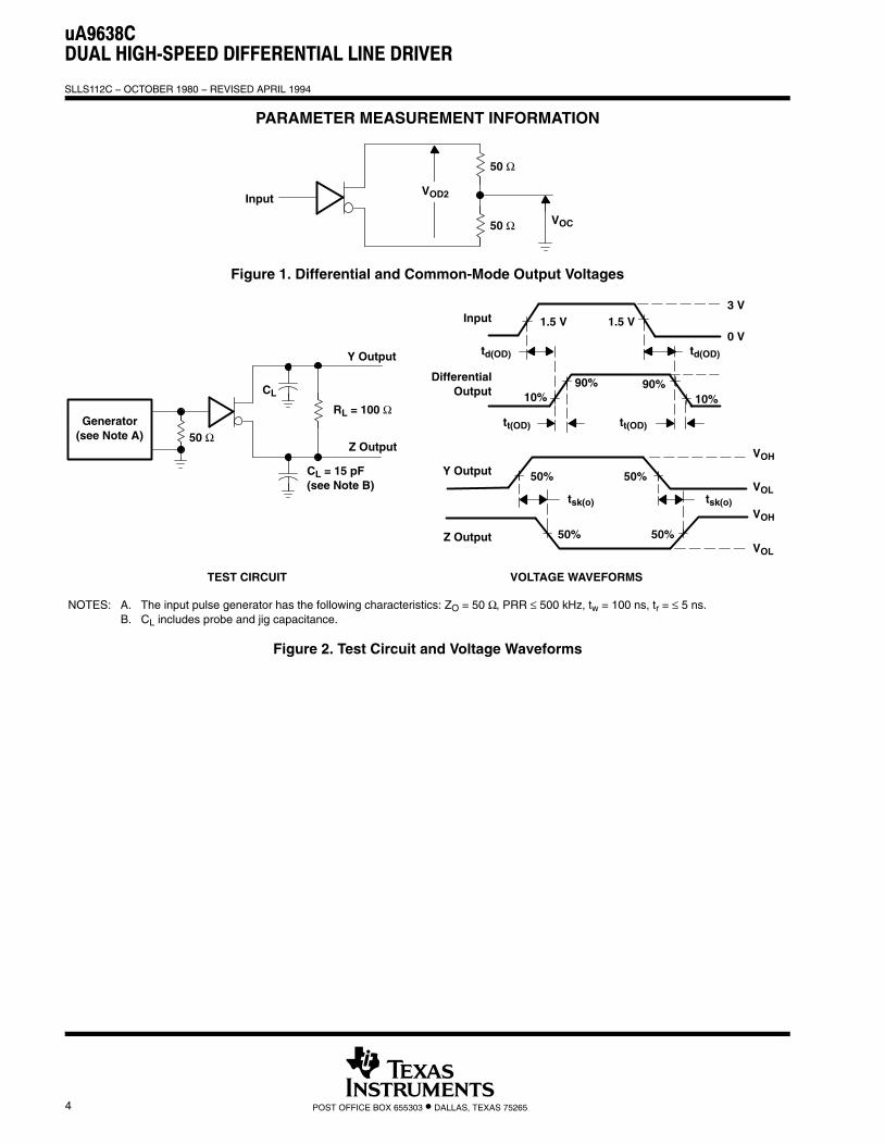
PARAMETER MEASUREMENT INFORMATION
50 Ω VOC
50 Ω
InputVOD2
Figure 1. Differential and Common-Mode Output Voltages
DifferentialOutput
td(OD)
TEST CIRCUIT
Z Output
CL = 15 pF(see Note B)
50 Ω
VOLTAGE WAVEFORMS
Input 1.5 V3 V
tt(OD)
0 Vtd(OD)
10% 10%90% 90%
Y Output
RL = 100 Ω
CL
1.5 V
tt(OD)
VOL50%
VOL
50%
tsk(o) tsk(o)
Y Output
Z Output
VOH
VOH
Generator(see Note A)
50% 50%
NOTES: A. The input pulse generator has the following characteristics: ZO = 50 Ω, PRR ≤ 500 kHz, tw = 100 ns, tr = ≤ 5 ns.B. CL includes probe and jig capacitance.
Figure 2. Test Circuit and Voltage Waveforms
PACKAGE OPTION ADDENDUM
www.ti.com 10-Jun-2014
Addendum-Page 1
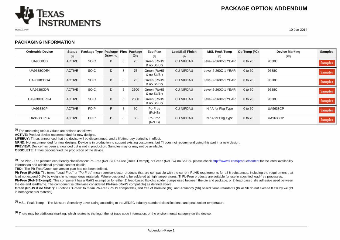
PACKAGING INFORMATION
Orderable Device Status(1)
Package Type PackageDrawing
Pins PackageQty
Eco Plan(2)
Lead/Ball Finish(6)
MSL Peak Temp(3)
Op Temp (°C) Device Marking(4/5)
Samples
UA9638CD ACTIVE SOIC D 8 75 Green (RoHS& no Sb/Br)
CU NIPDAU Level-2-260C-1 YEAR 0 to 70 9638C
UA9638CDE4 ACTIVE SOIC D 8 75 Green (RoHS& no Sb/Br)
CU NIPDAU Level-2-260C-1 YEAR 0 to 70 9638C
UA9638CDG4 ACTIVE SOIC D 8 75 Green (RoHS& no Sb/Br)
CU NIPDAU Level-2-260C-1 YEAR 0 to 70 9638C
UA9638CDR ACTIVE SOIC D 8 2500 Green (RoHS& no Sb/Br)
CU NIPDAU Level-2-260C-1 YEAR 0 to 70 9638C
UA9638CDRG4 ACTIVE SOIC D 8 2500 Green (RoHS& no Sb/Br)
CU NIPDAU Level-2-260C-1 YEAR 0 to 70 9638C
UA9638CP ACTIVE PDIP P 8 50 Pb-Free(RoHS)
CU NIPDAU N / A for Pkg Type 0 to 70 UA9638CP
UA9638CPE4 ACTIVE PDIP P 8 50 Pb-Free(RoHS)
CU NIPDAU N / A for Pkg Type 0 to 70 UA9638CP
(1) The marketing status values are defined as follows:ACTIVE: Product device recommended for new designs.LIFEBUY: TI has announced that the device will be discontinued, and a lifetime-buy period is in effect.NRND: Not recommended for new designs. Device is in production to support existing customers, but TI does not recommend using this part in a new design.PREVIEW: Device has been announced but is not in production. Samples may or may not be available.OBSOLETE: TI has discontinued the production of the device.
(2) Eco Plan - The planned eco-friendly classification: Pb-Free (RoHS), Pb-Free (RoHS Exempt), or Green (RoHS & no Sb/Br) - please check http://www.ti.com/productcontent for the latest availabilityinformation and additional product content details.TBD: The Pb-Free/Green conversion plan has not been defined.Pb-Free (RoHS): TI's terms "Lead-Free" or "Pb-Free" mean semiconductor products that are compatible with the current RoHS requirements for all 6 substances, including the requirement thatlead not exceed 0.1% by weight in homogeneous materials. Where designed to be soldered at high temperatures, TI Pb-Free products are suitable for use in specified lead-free processes.Pb-Free (RoHS Exempt): This component has a RoHS exemption for either 1) lead-based flip-chip solder bumps used between the die and package, or 2) lead-based die adhesive used betweenthe die and leadframe. The component is otherwise considered Pb-Free (RoHS compatible) as defined above.Green (RoHS & no Sb/Br): TI defines "Green" to mean Pb-Free (RoHS compatible), and free of Bromine (Br) and Antimony (Sb) based flame retardants (Br or Sb do not exceed 0.1% by weightin homogeneous material)
(3) MSL, Peak Temp. - The Moisture Sensitivity Level rating according to the JEDEC industry standard classifications, and peak solder temperature.
(4) There may be additional marking, which relates to the logo, the lot trace code information, or the environmental category on the device.
PACKAGE OPTION ADDENDUM
www.ti.com 10-Jun-2014
Addendum-Page 2
(5) Multiple Device Markings will be inside parentheses. Only one Device Marking contained in parentheses and separated by a "~" will appear on a device. If a line is indented then it is a continuationof the previous line and the two combined represent the entire Device Marking for that device.
(6) Lead/Ball Finish - Orderable Devices may have multiple material finish options. Finish options are separated by a vertical ruled line. Lead/Ball Finish values may wrap to two lines if the finishvalue exceeds the maximum column width.
Important Information and Disclaimer:The information provided on this page represents TI's knowledge and belief as of the date that it is provided. TI bases its knowledge and belief on informationprovided by third parties, and makes no representation or warranty as to the accuracy of such information. Efforts are underway to better integrate information from third parties. TI has taken andcontinues to take reasonable steps to provide representative and accurate information but may not have conducted destructive testing or chemical analysis on incoming materials and chemicals.TI and TI suppliers consider certain information to be proprietary, and thus CAS numbers and other limited information may not be available for release.
In no event shall TI's liability arising out of such information exceed the total purchase price of the TI part(s) at issue in this document sold by TI to Customer on an annual basis.
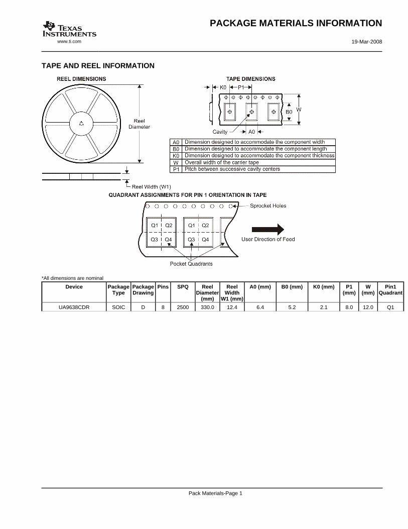
TAPE AND REEL INFORMATION
*All dimensions are nominal
Device PackageType
PackageDrawing
Pins SPQ ReelDiameter
(mm)
ReelWidth
W1 (mm)
A0 (mm) B0 (mm) K0 (mm) P1(mm)
W(mm)
Pin1Quadrant
UA9638CDR SOIC D 8 2500 330.0 12.4 6.4 5.2 2.1 8.0 12.0 Q1
PACKAGE MATERIALS INFORMATION
www.ti.com 19-Mar-2008
Pack Materials-Page 1
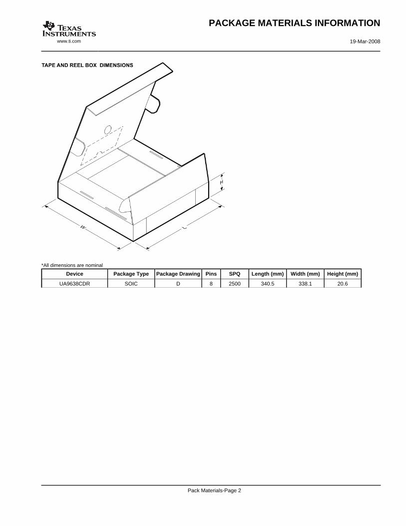
*All dimensions are nominal
Device Package Type Package Drawing Pins SPQ Length (mm) Width (mm) Height (mm)
UA9638CDR SOIC D 8 2500 340.5 338.1 20.6
PACKAGE MATERIALS INFORMATION
www.ti.com 19-Mar-2008
Pack Materials-Page 2

IMPORTANT NOTICE
Texas Instruments Incorporated and its subsidiaries (TI) reserve the right to make corrections, enhancements, improvements and otherchanges to its semiconductor products and services per JESD46, latest issue, and to discontinue any product or service per JESD48, latestissue. Buyers should obtain the latest relevant information before placing orders and should verify that such information is current andcomplete. All semiconductor products (also referred to herein as “components”) are sold subject to TI’s terms and conditions of salesupplied at the time of order acknowledgment.TI warrants performance of its components to the specifications applicable at the time of sale, in accordance with the warranty in TI’s termsand conditions of sale of semiconductor products. Testing and other quality control techniques are used to the extent TI deems necessaryto support this warranty. Except where mandated by applicable law, testing of all parameters of each component is not necessarilyperformed.TI assumes no liability for applications assistance or the design of Buyers’ products. Buyers are responsible for their products andapplications using TI components. To minimize the risks associated with Buyers’ products and applications, Buyers should provideadequate design and operating safeguards.TI does not warrant or represent that any license, either express or implied, is granted under any patent right, copyright, mask work right, orother intellectual property right relating to any combination, machine, or process in which TI components or services are used. Informationpublished by TI regarding third-party products or services does not constitute a license to use such products or services or a warranty orendorsement thereof. Use of such information may require a license from a third party under the patents or other intellectual property of thethird party, or a license from TI under the patents or other intellectual property of TI.Reproduction of significant portions of TI information in TI data books or data sheets is permissible only if reproduction is without alterationand is accompanied by all associated warranties, conditions, limitations, and notices. TI is not responsible or liable for such altereddocumentation. Information of third parties may be subject to additional restrictions.Resale of TI components or services with statements different from or beyond the parameters stated by TI for that component or servicevoids all express and any implied warranties for the associated TI component or service and is an unfair and deceptive business practice.TI is not responsible or liable for any such statements.Buyer acknowledges and agrees that it is solely responsible for compliance with all legal, regulatory and safety-related requirementsconcerning its products, and any use of TI components in its applications, notwithstanding any applications-related information or supportthat may be provided by TI. Buyer represents and agrees that it has all the necessary expertise to create and implement safeguards whichanticipate dangerous consequences of failures, monitor failures and their consequences, lessen the likelihood of failures that might causeharm and take appropriate remedial actions. Buyer will fully indemnify TI and its representatives against any damages arising out of the useof any TI components in safety-critical applications.In some cases, TI components may be promoted specifically to facilitate safety-related applications. With such components, TI’s goal is tohelp enable customers to design and create their own end-product solutions that meet applicable functional safety standards andrequirements. Nonetheless, such components are subject to these terms.No TI components are authorized for use in FDA Class III (or similar life-critical medical equipment) unless authorized officers of the partieshave executed a special agreement specifically governing such use.Only those TI components which TI has specifically designated as military grade or “enhanced plastic” are designed and intended for use inmilitary/aerospace applications or environments. Buyer acknowledges and agrees that any military or aerospace use of TI componentswhich have not been so designated is solely at the Buyer's risk, and that Buyer is solely responsible for compliance with all legal andregulatory requirements in connection with such use.TI has specifically designated certain components as meeting ISO/TS16949 requirements, mainly for automotive use. In any case of use ofnon-designated products, TI will not be responsible for any failure to meet ISO/TS16949.
Products ApplicationsAudio www.ti.com/audio Automotive and Transportation www.ti.com/automotiveAmplifiers amplifier.ti.com Communications and Telecom www.ti.com/communicationsData Converters dataconverter.ti.com Computers and Peripherals www.ti.com/computersDLP® Products www.dlp.com Consumer Electronics www.ti.com/consumer-appsDSP dsp.ti.com Energy and Lighting www.ti.com/energyClocks and Timers www.ti.com/clocks Industrial www.ti.com/industrialInterface interface.ti.com Medical www.ti.com/medicalLogic logic.ti.com Security www.ti.com/securityPower Mgmt power.ti.com Space, Avionics and Defense www.ti.com/space-avionics-defenseMicrocontrollers microcontroller.ti.com Video and Imaging www.ti.com/videoRFID www.ti-rfid.comOMAP Applications Processors www.ti.com/omap TI E2E Community e2e.ti.comWireless Connectivity www.ti.com/wirelessconnectivity
Mailing Address: Texas Instruments, Post Office Box 655303, Dallas, Texas 75265Copyright © 2016, Texas Instruments Incorporated