Dual 4-A Peak High-Speed Low-Side Power-MOSFET … · 5 UCC27323, UCC27324, UCC27325 UCC37323,...
34
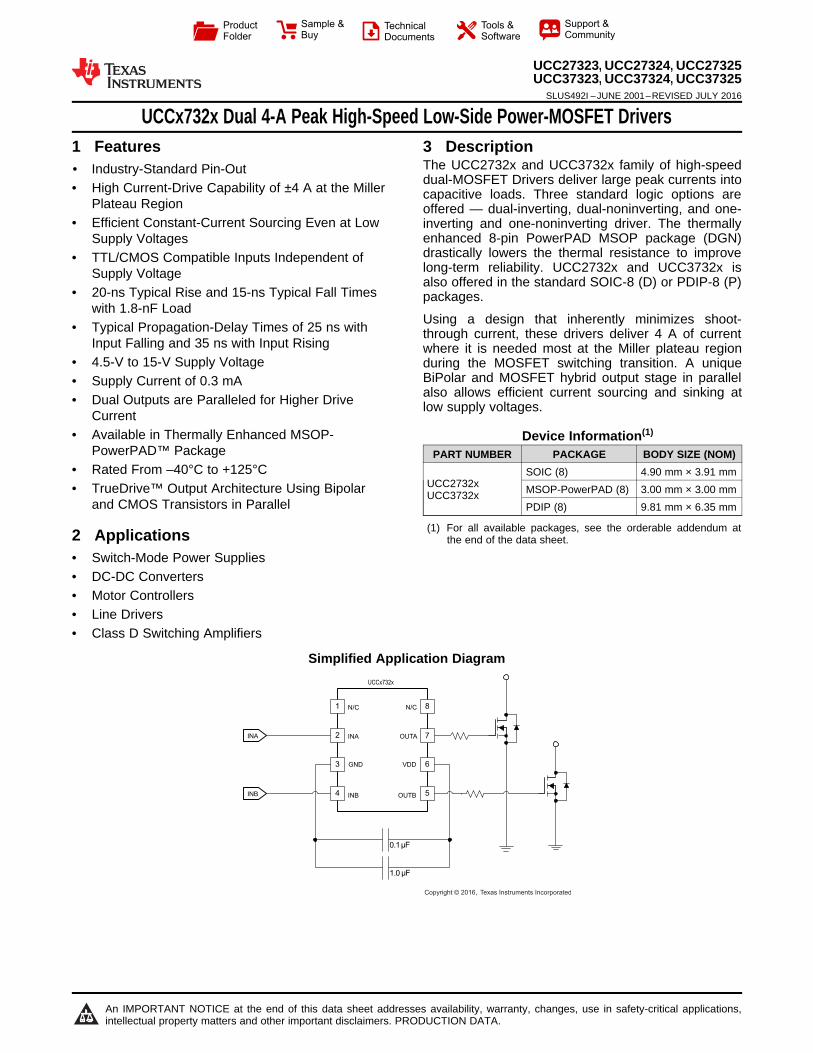
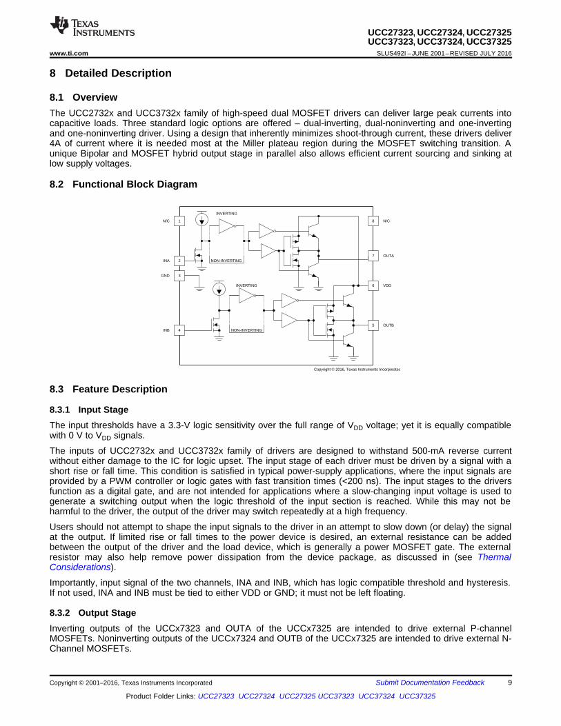
UCCx732x 1 2 3 4 8 7 6 5 N/C INA INB GND N/C OUTA OUTB VDD 0.1 μF INA INB 1.0 μF Copyright © 2016, Texas Instruments Incorporated Product Folder Sample & Buy Technical Documents Tools & Software Support & Community An IMPORTANT NOTICE at the end of this data sheet addresses availability, warranty, changes, use in safety-critical applications, intellectual property matters and other important disclaimers. PRODUCTION DATA. UCC27323, UCC27324, UCC27325 UCC37323, UCC37324, UCC37325 SLUS492I – JUNE 2001 – REVISED JULY 2016 UCCx732x Dual 4-A Peak High-Speed Low-Side Power-MOSFET Drivers 1 1 Features 1• Industry-Standard Pin-Out • High Current-Drive Capability of ±4 A at the Miller Plateau Region • Efficient Constant-Current Sourcing Even at Low Supply Voltages • TTL/CMOS Compatible Inputs Independent of Supply Voltage • 20-ns Typical Rise and 15-ns Typical Fall Times with 1.8-nF Load • Typical Propagation-Delay Times of 25 ns with Input Falling and 35 ns with Input Rising • 4.5-V to 15-V Supply Voltage • Supply Current of 0.3 mA • Dual Outputs are Paralleled for Higher Drive Current • Available in Thermally Enhanced MSOP- PowerPAD™ Package • Rated From –40°C to +125°C • TrueDrive™ Output Architecture Using Bipolar and CMOS Transistors in Parallel 2 Applications • Switch-Mode Power Supplies • DC-DC Converters • Motor Controllers • Line Drivers • Class D Switching Amplifiers 3 Description The UCC2732x and UCC3732x family of high-speed dual-MOSFET Drivers deliver large peak currents into capacitive loads. Three standard logic options are offered — dual-inverting, dual-noninverting, and one- inverting and one-noninverting driver. The thermally enhanced 8-pin PowerPAD MSOP package (DGN) drastically lowers the thermal resistance to improve long-term reliability. UCC2732x and UCC3732x is also offered in the standard SOIC-8 (D) or PDIP-8 (P) packages. Using a design that inherently minimizes shoot- through current, these drivers deliver 4 A of current where it is needed most at the Miller plateau region during the MOSFET switching transition. A unique BiPolar and MOSFET hybrid output stage in parallel also allows efficient current sourcing and sinking at low supply voltages. Device Information (1) PART NUMBER PACKAGE BODY SIZE (NOM) UCC2732x UCC3732x SOIC (8) 4.90 mm × 3.91 mm MSOP-PowerPAD (8) 3.00 mm × 3.00 mm PDIP (8) 9.81 mm × 6.35 mm (1) For all available packages, see the orderable addendum at the end of the data sheet. Simplified Application Diagram
Transcript of Dual 4-A Peak High-Speed Low-Side Power-MOSFET … · 5 UCC27323, UCC27324, UCC27325 UCC37323,...
UCCx732x
1
2
3
4
8
7
6
5
N/C
INA
INB
GND
N/C
OUTA
OUTB
VDD
0.1μF
INA
INB
1.0 μF
Copyright © 2016, Texas Instruments Incorporated
Product
Folder
Sample &Buy
Technical
Documents
Tools &
Software
Support &Community
An IMPORTANT NOTICE at the end of this data sheet addresses availability, warranty, changes, use in safety-critical applications,intellectual property matters and other important disclaimers. PRODUCTION DATA.
UCC27323, UCC27324, UCC27325UCC37323, UCC37324, UCC37325
SLUS492I –JUNE 2001–REVISED JULY 2016
UCCx732x Dual 4-A Peak High-Speed Low-Side Power-MOSFET Drivers
1
1 Features1• Industry-Standard Pin-Out• High Current-Drive Capability of ±4 A at the Miller
Plateau Region• Efficient Constant-Current Sourcing Even at Low
Supply Voltages• TTL/CMOS Compatible Inputs Independent of
Supply Voltage• 20-ns Typical Rise and 15-ns Typical Fall Times
with 1.8-nF Load• Typical Propagation-Delay Times of 25 ns with
Input Falling and 35 ns with Input Rising• 4.5-V to 15-V Supply Voltage• Supply Current of 0.3 mA• Dual Outputs are Paralleled for Higher Drive
Current• Available in Thermally Enhanced MSOP-
PowerPAD™ Package• Rated From –40°C to +125°C• TrueDrive™ Output Architecture Using Bipolar
and CMOS Transistors in Parallel
2 Applications• Switch-Mode Power Supplies• DC-DC Converters• Motor Controllers• Line Drivers• Class D Switching Amplifiers
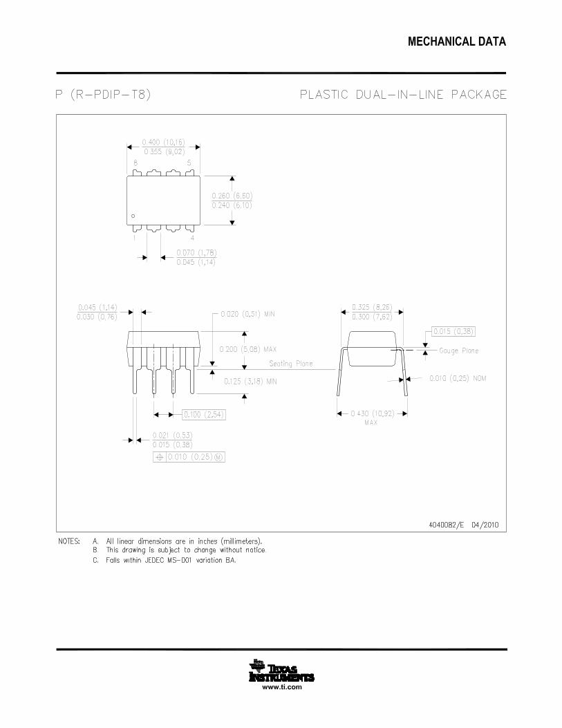
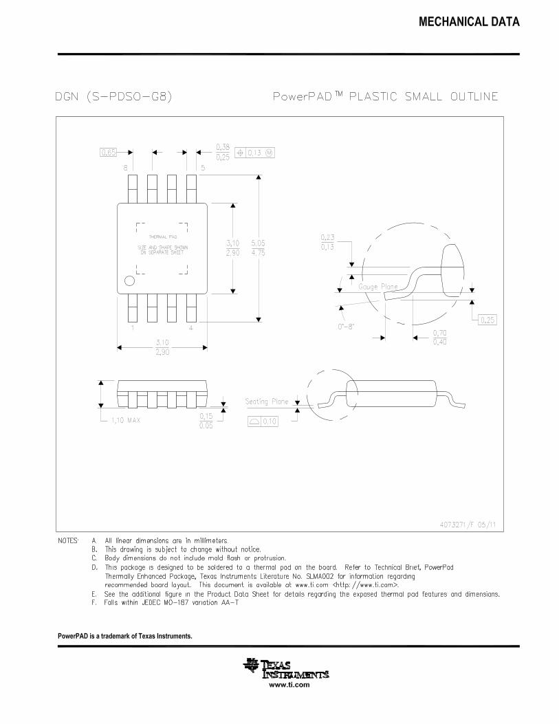
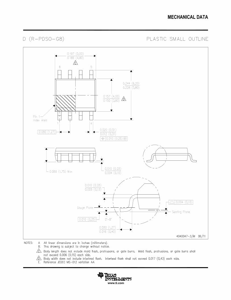
3 DescriptionThe UCC2732x and UCC3732x family of high-speeddual-MOSFET Drivers deliver large peak currents intocapacitive loads. Three standard logic options areoffered — dual-inverting, dual-noninverting, and one-inverting and one-noninverting driver. The thermallyenhanced 8-pin PowerPAD MSOP package (DGN)drastically lowers the thermal resistance to improvelong-term reliability. UCC2732x and UCC3732x isalso offered in the standard SOIC-8 (D) or PDIP-8 (P)packages.
Using a design that inherently minimizes shoot-through current, these drivers deliver 4 A of currentwhere it is needed most at the Miller plateau regionduring the MOSFET switching transition. A uniqueBiPolar and MOSFET hybrid output stage in parallelalso allows efficient current sourcing and sinking atlow supply voltages.
Device Information(1)
PART NUMBER PACKAGE BODY SIZE (NOM)
UCC2732xUCC3732x
SOIC (8) 4.90 mm × 3.91 mmMSOP-PowerPAD (8) 3.00 mm × 3.00 mmPDIP (8) 9.81 mm × 6.35 mm
(1) For all available packages, see the orderable addendum atthe end of the data sheet.
Simplified Application Diagram
2
UCC27323, UCC27324, UCC27325UCC37323, UCC37324, UCC37325SLUS492I –JUNE 2001–REVISED JULY 2016 www.ti.com
Product Folder Links: UCC27323 UCC27324 UCC27325 UCC37323 UCC37324 UCC37325
Submit Documentation Feedback Copyright © 2001–2016, Texas Instruments Incorporated
Table of Contents1 Features .................................................................. 12 Applications ........................................................... 13 Description ............................................................. 14 Revision History..................................................... 25 Device Comparison Table ..................................... 36 Pin Configuration and Functions ......................... 47 Specifications......................................................... 5
7.1 Absolute Maximum Ratings ...................................... 57.2 ESD Ratings.............................................................. 57.3 Recommended Operating Conditions....................... 57.4 Thermal Information .................................................. 57.5 Electrical Characteristics........................................... 67.6 Switching Characteristics .......................................... 67.7 Typical Characteristics .............................................. 8
8 Detailed Description .............................................. 98.1 Overview ................................................................... 98.2 Functional Block Diagram ......................................... 98.3 Feature Description................................................... 9
8.4 Device Functional Modes........................................ 109 Application and Implementation ........................ 11
9.1 Application Information............................................ 119.2 Typical Application ................................................. 12
10 Power Supply Recommendations ..................... 1611 Layout................................................................... 17
11.1 Layout Guidelines ................................................. 1711.2 Layout Example .................................................... 1711.3 Thermal Considerations ........................................ 18
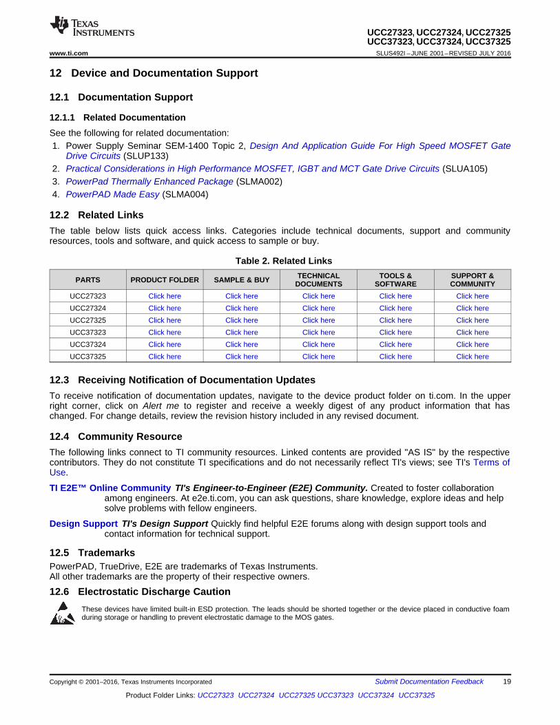
12 Device and Documentation Support ................. 1912.1 Documentation Support ........................................ 1912.2 Related Links ........................................................ 1912.3 Receiving Notification of Documentation Updates 1912.4 Community Resource............................................ 1912.5 Trademarks ........................................................... 1912.6 Electrostatic Discharge Caution............................ 1912.7 Glossary ................................................................ 20
13 Mechanical, Packaging, and OrderableInformation ........................................................... 20
4 Revision HistoryNOTE: Page numbers for previous revisions may differ from page numbers in the current version.
Changes from Revision H (May 2013) to Revision I Page
• Added ESD Ratings table, Feature Description section, Device Functional Modes, Application and Implementationsection, Power Supply Recommendations section, Layout section, Device and Documentation Support section, andMechanical, Packaging, and Orderable Information section ................................................................................................. 1
• Deleted Power Dissipation rows from Absolute Maximum Ratings ...................................................................................... 5
Changes from Revision G (March 2010) to Revision H Page
• Changed DSCHOTTKY diode direction and voltage of zener diode from 5.5 to 4.5 V in Figure 7............................................ 13• Added three paragraphs after first paragraph of Operational Waveforms and Circuit Layout section before Figure 9....... 16
3
UCC27323, UCC27324, UCC27325UCC37323, UCC37324, UCC37325
www.ti.com SLUS492I –JUNE 2001–REVISED JULY 2016
Product Folder Links: UCC27323 UCC27324 UCC27325 UCC37323 UCC37324 UCC37325
Submit Documentation FeedbackCopyright © 2001–2016, Texas Instruments Incorporated
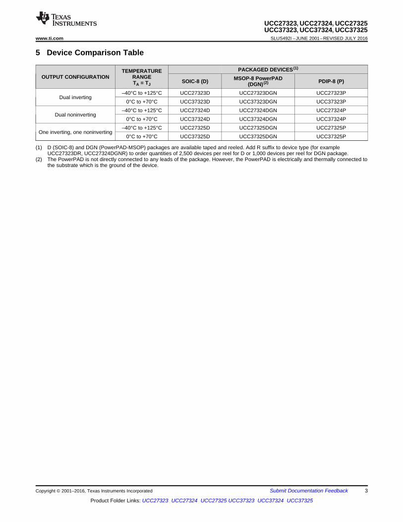
(1) D (SOIC-8) and DGN (PowerPAD-MSOP) packages are available taped and reeled. Add R suffix to device type (for exampleUCC27323DR, UCC27324DGNR) to order quantities of 2,500 devices per reel for D or 1,000 devices per reel for DGN package.
(2) The PowerPAD is not directly connected to any leads of the package. However, the PowerPAD is electrically and thermally connected tothe substrate which is the ground of the device.
5 Device Comparison Table
OUTPUT CONFIGURATIONTEMPERATURE
RANGETA = TJ
PACKAGED DEVICES (1)
SOIC-8 (D) MSOP-8 PowerPAD(DGN) (2) PDIP-8 (P)
Dual inverting–40°C to +125°C UCC27323D UCC27323DGN UCC27323P
0°C to +70°C UCC37323D UCC37323DGN UCC37323P
Dual noninverting–40°C to +125°C UCC27324D UCC27324DGN UCC27324P
0°C to +70°C UCC37324D UCC37324DGN UCC37324P
One inverting, one noninverting–40°C to +125°C UCC27325D UCC27325DGN UCC27325P
0°C to +70°C UCC37325D UCC37325DGN UCC37325P
4
UCC27323, UCC27324, UCC27325UCC37323, UCC37324, UCC37325SLUS492I –JUNE 2001–REVISED JULY 2016 www.ti.com
Product Folder Links: UCC27323 UCC27324 UCC27325 UCC37323 UCC37324 UCC37325
Submit Documentation Feedback Copyright © 2001–2016, Texas Instruments Incorporated
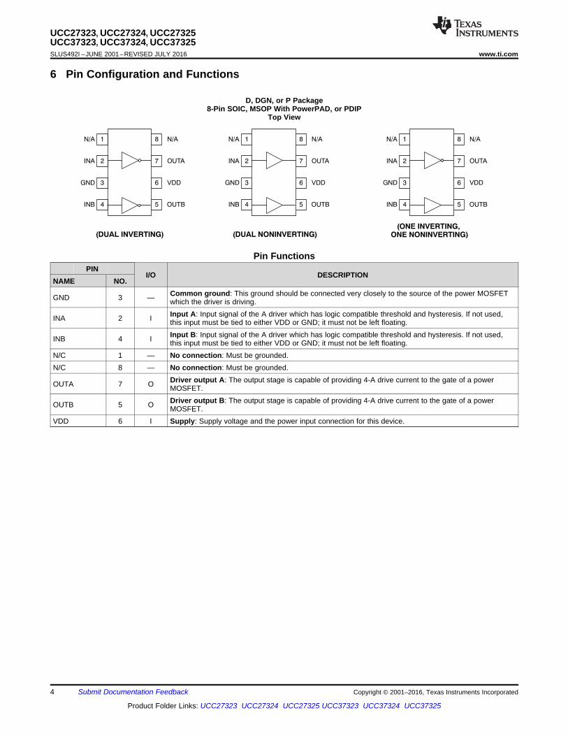
6 Pin Configuration and Functions
D, DGN, or P Package8-Pin SOIC, MSOP With PowerPAD, or PDIP
Top View
Pin FunctionsPIN
I/O DESCRIPTIONNAME NO.
GND 3 — Common ground: This ground should be connected very closely to the source of the power MOSFETwhich the driver is driving.
INA 2 I Input A: Input signal of the A driver which has logic compatible threshold and hysteresis. If not used,this input must be tied to either VDD or GND; it must not be left floating.
INB 4 I Input B: Input signal of the A driver which has logic compatible threshold and hysteresis. If not used,this input must be tied to either VDD or GND; it must not be left floating.
N/C 1 — No connection: Must be grounded.N/C 8 — No connection: Must be grounded.
OUTA 7 O Driver output A: The output stage is capable of providing 4-A drive current to the gate of a powerMOSFET.
OUTB 5 O Driver output B: The output stage is capable of providing 4-A drive current to the gate of a powerMOSFET.
VDD 6 I Supply: Supply voltage and the power input connection for this device.
5
UCC27323, UCC27324, UCC27325UCC37323, UCC37324, UCC37325
www.ti.com SLUS492I –JUNE 2001–REVISED JULY 2016
Product Folder Links: UCC27323 UCC27324 UCC27325 UCC37323 UCC37324 UCC37325
Submit Documentation FeedbackCopyright © 2001–2016, Texas Instruments Incorporated
(1) Stresses beyond those listed under Absolute Maximum Ratings may cause permanent damage to the device. These are stress ratingsonly, which do not imply functional operation of the device at these or any other conditions beyond those indicated under RecommendedOperating Conditions. Exposure to absolute-maximum-rated conditions for extended periods may affect device reliability.
(2) All voltages are with respect to GND. Currents are positive into, negative out of the specified terminal.
7 Specifications
7.1 Absolute Maximum Ratingsover operating free-air temperature range (unless otherwise noted) (1) (2)
MIN MAX UNITAnalog input voltage (INA, INB) –0.3 to VDD + 0.3 V not to exceed 16 VOutput body diode DC current (OUTA, OUTB) 0.2
AIOUT_DCIOUT_PULSED
Output current (OUTA, OUTB)DC 0.2Pulsed (0.5 µs) 4.5
Output voltage (OUTA, OUTB) 16 VVDD Supply voltage –0.3 16 VTJ Junction operating temperature –55 150
°CTstg Storage temperature –65 150
(1) JEDEC document JEP155 states that 500-V HBM allows safe manufacturing with a standard ESD control process.(2) JEDEC document JEP157 states that 250-V CDM allows safe manufacturing with a standard ESD control process.
7.2 ESD RatingsVALUE UNIT
V(ESD) Electrostatic dischargeHuman-body model (HBM), per ANSI/ESDA/JEDEC JS-001 (1) 4000
VCharged-device model (CDM), per JEDEC specification JESD22-C101 (2) 1000
7.3 Recommended Operating Conditionsover operating free-air temperature range (unless otherwise noted)
MIN NOM MAX UNITSupply voltage 4.5 15 VInput voltage 0 15 V
Operating junction temperatureUCC2732x –40 125 °CUCC3732x 0 70 °C
(1) For more information about traditional and new thermal metrics, see the Semiconductor and IC Package Thermal Metrics applicationreport.
7.4 Thermal Information
THERMAL METRIC (1)
UCCx732x
UNITD(SOIC)
DGN(MSOP WithPowerPAD)
P(PDIP)
8 PINS 8 PINS 8 PINSRθJA Junction-to-ambient thermal resistance 107.3 56.6 55.5 °C/WRθJC(top) Junction-to-case (top) thermal resistance 52.2 52.8 45.3 °C/WRθJB Junction-to-board thermal resistance 47.3 32.6 32.6 °C/WψJT Junction-to-top characterization parameter 10.2 1.8 23 °C/WψJB Junction-to-board characterization parameter 46.8 32.3 32.5 °C/WRθJC(bot) Junction-to-case (bottom) thermal resistance N/A 5.9 N/A °C/W
6
UCC27323, UCC27324, UCC27325UCC37323, UCC37324, UCC37325SLUS492I –JUNE 2001–REVISED JULY 2016 www.ti.com
Product Folder Links: UCC27323 UCC27324 UCC27325 UCC37323 UCC37324 UCC37325
Submit Documentation Feedback Copyright © 2001–2016, Texas Instruments Incorporated
(1) The pullup and pulldown circuits of the driver are bipolar and MOSFET transistors in parallel. The pulsed output current rating is thecombined current from the bipolar and MOSFET transistors.
(2) The pullup and pulldown circuits of the driver are bipolar and MOSFET transistors in parallel. The output resistance is the RDS(ON) of theMOSFET transistor when the voltage on the driver output is less than the saturation voltage of the bipolar transistor.
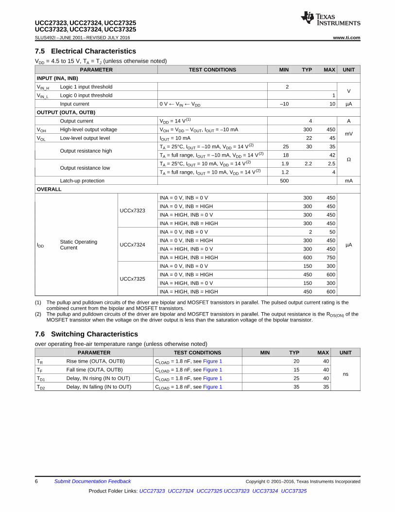
7.5 Electrical CharacteristicsVDD = 4.5 to 15 V, TA = TJ (unless otherwise noted)
PARAMETER TEST CONDITIONS MIN TYP MAX UNITINPUT (INA, INB)VIN_H Logic 1 input threshold 2
VVIN_L Logic 0 input threshold 1
Input current 0 V ← VIN ← VDD –10 10 µAOUTPUT (OUTA, OUTB)
Output current VDD = 14 V (1) 4 AVOH High-level output voltage VOH = VDD – VOUT, IOUT = –10 mA 300 450
mVVOL Low-level output level IOUT = 10 mA 22 45
Output resistance highTA = 25°C, IOUT = –10 mA, VDD = 14 V (2) 25 30 35
ΩTA = full range, IOUT = –10 mA, VDD = 14 V (2) 18 42
Output resistance lowTA = 25°C, IOUT = 10 mA, VDD = 14 V (2) 1.9 2.2 2.5TA = full range, IOUT = 10 mA, VDD = 14 V (2) 1.2 4
Latch-up protection 500 mAOVERALL
IDDStatic OperatingCurrent
UCCx7323
INA = 0 V, INB = 0 V 300 450
µA
INA = 0 V, INB = HIGH 300 450INA = HIGH, INB = 0 V 300 450INA = HIGH, INB = HIGH 300 450
UCCx7324
INA = 0 V, INB = 0 V 2 50INA = 0 V, INB = HIGH 300 450INA = HIGH, INB = 0 V 300 450INA = HIGH, INB = HIGH 600 750
UCCx7325
INA = 0 V, INB = 0 V 150 300INA = 0 V, INB = HIGH 450 600INA = HIGH, INB = 0 V 150 300INA = HIGH, INB = HIGH 450 600
7.6 Switching Characteristicsover operating free-air temperature range (unless otherwise noted)
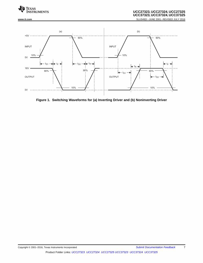
PARAMETER TEST CONDITIONS MIN TYP MAX UNITTR Rise time (OUTA, OUTB) CLOAD = 1.8 nF, see Figure 1 20 40
nsTF Fall time (OUTA, OUTB) CLOAD = 1.8 nF, see Figure 1 15 40TD1 Delay, IN rising (IN to OUT) CLOAD = 1.8 nF, see Figure 1 25 40TD2 Delay, IN falling (IN to OUT) CLOAD = 1.8 nF, see Figure 1 35 35
+5V
INPUT
16V
OUTPUT
0V
0V
10%
90%
10%
90%
(a)
90%
90%
10%
90%
(b)
INPUT
OUTPUT
10%
tD1 tD2tF tR
tD1
tR
tF
tD2
7
UCC27323, UCC27324, UCC27325UCC37323, UCC37324, UCC37325
www.ti.com SLUS492I –JUNE 2001–REVISED JULY 2016
Product Folder Links: UCC27323 UCC27324 UCC27325 UCC37323 UCC37324 UCC37325
Submit Documentation FeedbackCopyright © 2001–2016, Texas Instruments Incorporated
Figure 1. Switching Waveforms for (a) Inverting Driver and (b) Noninverting Driver
-501.2
1.3
1.4
1.5
1.6
1.7
1.8
1.9
2.0
125-25 0 25 50 10075
VO
N-
Inp
ut
Th
resh
old
Vo
ltag
e -
V
TJ - Temperature - °C
VDD = 15 V
VDD = 10 V
VDD = 4.5 V
12
14
16
18
20
22
30
24
26
28
VDD - Supply Voltage - V
tD1 -
Dela
y T
ime -
ns
1 nF
4.7 nF
2.2 nF
10 nF
470 pF
4 10 1686 12 14
tD2 -
Dela
y T
ime -
ns
VDD - Supply Voltage - V
20
22
24
26
32
34
38
28
30
36
1 nF
4.7 nF
2.2 nF
10 nF
470 pF
4 10 1686 12 14
8
UCC27323, UCC27324, UCC27325UCC37323, UCC37324, UCC37325SLUS492I –JUNE 2001–REVISED JULY 2016 www.ti.com
Product Folder Links: UCC27323 UCC27324 UCC27325 UCC37323 UCC37324 UCC37325
Submit Documentation Feedback Copyright © 2001–2016, Texas Instruments Incorporated
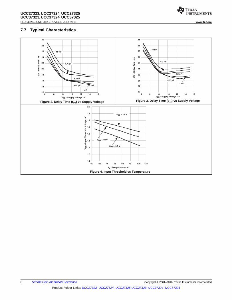
7.7 Typical Characteristics
Figure 2. Delay Time (tD1) vs Supply Voltage Figure 3. Delay Time (tD2) vs Supply Voltage
Figure 4. Input Threshold vs Temperature
1
OUTA
N/C
2INA
3GND
7
N/C8
INVERTING
NON-INVERTING
OUTB4
5
INVERTING
NON-INVERTINGINB
6 VDD
Copyright © 2016, Texas Instruments Incorporated
9
UCC27323, UCC27324, UCC27325UCC37323, UCC37324, UCC37325
www.ti.com SLUS492I –JUNE 2001–REVISED JULY 2016
Product Folder Links: UCC27323 UCC27324 UCC27325 UCC37323 UCC37324 UCC37325
Submit Documentation FeedbackCopyright © 2001–2016, Texas Instruments Incorporated
8 Detailed Description
8.1 OverviewThe UCC2732x and UCC3732x family of high-speed dual MOSFET drivers can deliver large peak currents intocapacitive loads. Three standard logic options are offered – dual-inverting, dual-noninverting and one-invertingand one-noninverting driver. Using a design that inherently minimizes shoot-through current, these drivers deliver4A of current where it is needed most at the Miller plateau region during the MOSFET switching transition. Aunique Bipolar and MOSFET hybrid output stage in parallel also allows efficient current sourcing and sinking atlow supply voltages.
8.2 Functional Block Diagram
8.3 Feature Description
8.3.1 Input StageThe input thresholds have a 3.3-V logic sensitivity over the full range of VDD voltage; yet it is equally compatiblewith 0 V to VDD signals.
The inputs of UCC2732x and UCC3732x family of drivers are designed to withstand 500-mA reverse currentwithout either damage to the IC for logic upset. The input stage of each driver must be driven by a signal with ashort rise or fall time. This condition is satisfied in typical power-supply applications, where the input signals areprovided by a PWM controller or logic gates with fast transition times (<200 ns). The input stages to the driversfunction as a digital gate, and are not intended for applications where a slow-changing input voltage is used togenerate a switching output when the logic threshold of the input section is reached. While this may not beharmful to the driver, the output of the driver may switch repeatedly at a high frequency.
Users should not attempt to shape the input signals to the driver in an attempt to slow down (or delay) the signalat the output. If limited rise or fall times to the power device is desired, an external resistance can be addedbetween the output of the driver and the load device, which is generally a power MOSFET gate. The externalresistor may also help remove power dissipation from the device package, as discussed in (see ThermalConsiderations).
Importantly, input signal of the two channels, INA and INB, which has logic compatible threshold and hysteresis.If not used, INA and INB must be tied to either VDD or GND; it must not be left floating.
8.3.2 Output StageInverting outputs of the UCCx7323 and OUTA of the UCCx7325 are intended to drive external P-channelMOSFETs. Noninverting outputs of the UCCx7324 and OUTB of the UCCx7325 are intended to drive external N-Channel MOSFETs.
10
UCC27323, UCC27324, UCC27325UCC37323, UCC37324, UCC37325SLUS492I –JUNE 2001–REVISED JULY 2016 www.ti.com
Product Folder Links: UCC27323 UCC27324 UCC27325 UCC37323 UCC37324 UCC37325
Submit Documentation Feedback Copyright © 2001–2016, Texas Instruments Incorporated
Feature Description (continued)Each output stage is capable of supplying ±4-A peak current pulses and swings to both VDD and GND. Thepullup and pulldown circuits of the driver are constructed of bipolar and MOSFET transistors in parallel. The peakoutput current rating is the combined current from the bipolar and MOSFET transistors. The output resistance isthe RDS(on) of the MOSFET transistor when the voltage on the driver output is less than the saturation voltage ofthe bipolar transistor. Each output stage also provides a very low impedance to overshoot and undershoot due tothe body diode of the external MOSFET.
This means that in many cases, external-Schottky-clamp diodes are not required. The UCCx732x family delivers4 A of gate drive where it is most needed during the MOSFET switching transition – at the Miller plateau region –providing improved efficiency gains. A unique Bipolar and MOSFET hybrid output stage in parallel also allowsefficient current sourcing at low supply voltages.
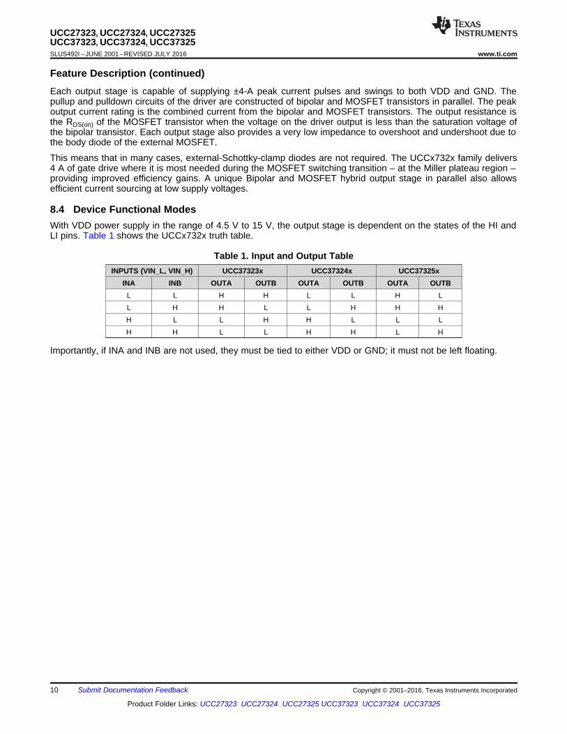
8.4 Device Functional ModesWith VDD power supply in the range of 4.5 V to 15 V, the output stage is dependent on the states of the HI andLI pins. Table 1 shows the UCCx732x truth table.
Table 1. Input and Output TableINPUTS (VIN_L, VIN_H) UCC37323x UCC37324x UCC37325x
INA INB OUTA OUTB OUTA OUTB OUTA OUTBL L H H L L H LL H H L L H H HH L L H H L L LH H L L H H L H
Importantly, if INA and INB are not used, they must be tied to either VDD or GND; it must not be left floating.
11
UCC27323, UCC27324, UCC27325UCC37323, UCC37324, UCC37325
www.ti.com SLUS492I –JUNE 2001–REVISED JULY 2016
Product Folder Links: UCC27323 UCC27324 UCC27325 UCC37323 UCC37324 UCC37325
Submit Documentation FeedbackCopyright © 2001–2016, Texas Instruments Incorporated
9 Application and Implementation
NOTEInformation in the following applications sections is not part of the TI componentspecification, and TI does not warrant its accuracy or completeness. TI’s customers areresponsible for determining suitability of components for their purposes. Customers shouldvalidate and test their design implementation to confirm system functionality.
9.1 Application InformationHigh-frequency power supplies often require high-speed, high-current drivers such as the UCCx732x family. Aleading application is the needed to provide a high-power buffer stage between the PWM output of the control ICand the gates of the primary power MOSFET or IGBT switching devices. In other cases, the driver IC is used todrive the power-device gates through a drive transformer. Synchronous rectification supplies are also needed tosimultaneously drive multiple devices which presents an extremely large load to the control circuitry.
Driver ICs are used when having the primary PWM regulator IC directly drive the switching devices for one ormore reasons is not feasible. The PWMIC does not have the brute drive capability required for the intendedswitching MOSFET, limiting the switching performance in the application. In other cases there may be a desire tominimize the effect of high-frequency switching noise by placing the high current driver physically close to theload. Also, newer ICs that target the highest operating frequencies do not incorporate onboard gate drivers at all.Their PWM outputs are only intended to drive the high impedance input to a driver such as the UCCx732x.Finally, the control IC is under thermal stress due to power dissipation, and an external driver helps by movingthe heat from the controller to an external package.
UCCx732x
1
2
3
4
8
7
6
5
N/C
INA
INB
GND
N/C
OUTA
OUTB
VDD
0.1μF
INA
INB
1.0 μF
Copyright © 2016, Texas Instruments Incorporated
12
UCC27323, UCC27324, UCC27325UCC37323, UCC37324, UCC37325SLUS492I –JUNE 2001–REVISED JULY 2016 www.ti.com
Product Folder Links: UCC27323 UCC27324 UCC27325 UCC37323 UCC37324 UCC37325
Submit Documentation Feedback Copyright © 2001–2016, Texas Instruments Incorporated
9.2 Typical Application
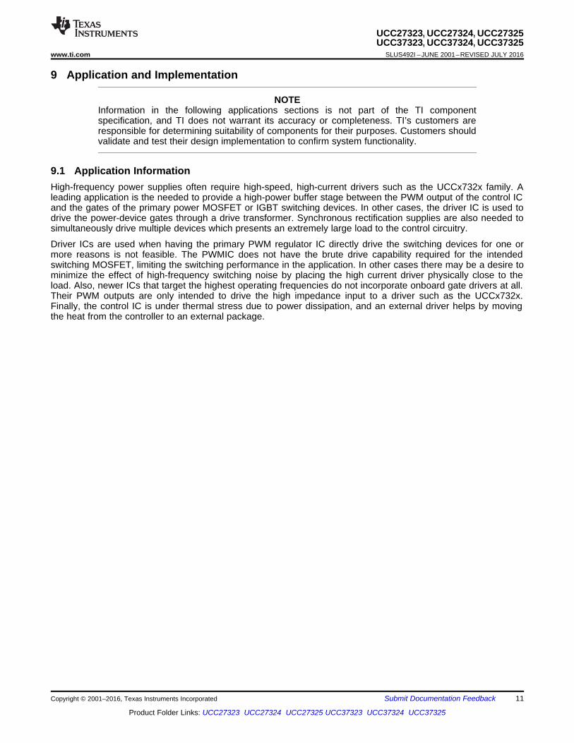
Figure 5. UCCx732x Driving Two Independent MOSFETs
9.2.1 Design RequirementsTo select proper device from UCCx732x family, TI recommends first checking the appropriate logic for theoutputs. UCCx7323 has dual inverting outputs; UCCx7324 has dual noninverting outputs; UCCx7325 haveinverting channel A and noninverting channel B. Moreover, some design considerations must be evaluated first inorder to make the most appropriate selection. Among these considerations are VDD, drive current, and powerdissipation.
9.2.2 Detailed Design Procedure
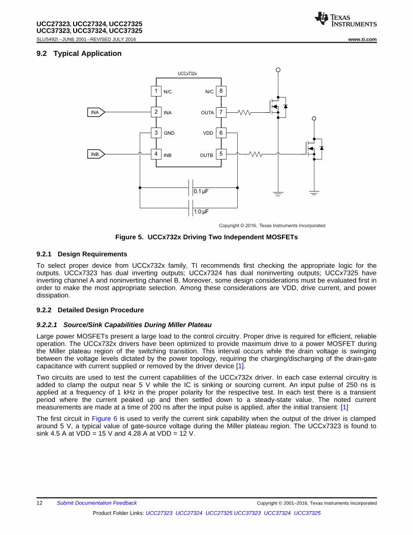
9.2.2.1 Source/Sink Capabilities During Miller PlateauLarge power MOSFETs present a large load to the control circuitry. Proper drive is required for efficient, reliableoperation. The UCCx732x drivers have been optimized to provide maximum drive to a power MOSFET duringthe Miller plateau region of the switching transition. This interval occurs while the drain voltage is swingingbetween the voltage levels dictated by the power topology, requiring the charging/discharging of the drain-gatecapacitance with current supplied or removed by the driver device [1].
Two circuits are used to test the current capabilities of the UCCx732x driver. In each case external circuitry isadded to clamp the output near 5 V while the IC is sinking or sourcing current. An input pulse of 250 ns isapplied at a frequency of 1 kHz in the proper polarity for the respective test. In each test there is a transientperiod where the current peaked up and then settled down to a steady-state value. The noted currentmeasurements are made at a time of 200 ns after the input pulse is applied, after the initial transient. [1]
The first circuit in Figure 6 is used to verify the current sink capability when the output of the driver is clampedaround 5 V, a typical value of gate-source voltage during the Miller plateau region. The UCCx7323 is found tosink 4.5 A at VDD = 15 V and 4.28 A at VDD = 12 V.
UCCx7323
1
2
3
4
8
7
6
5
N/C
INA
INB
GND
N/C
OUTA
OUTB
VDD
1 µF CER
AL EL
1 µF CERAL EL
10 Ω
RSNS
0.1 Ω
VSNS
DSCHOTTKY
VDD
4.5V
SignalGeneratorproducing
250 ns widepulse
100 µF
100 µF
Copywright © 2016, Texas Instruments Incorporated
UCCx7323
1
2
3
4
8
7
6
5
N/C N/C
INA
INB
GND
OUTA
OUTB
VDD
1 µF CER
100 µF
AL EL
1µF CER 100 µF
AL EL
VADJ
5.5V
10 Ω
RSNS
0.1 Ω
VSNS
Signal
Generator
producing
250 ns wide
pulse
DSCHOTTKY
VDD
Copyright © 2016, Texas Instruments Incorporated
13
UCC27323, UCC27324, UCC27325UCC37323, UCC37324, UCC37325
www.ti.com SLUS492I –JUNE 2001–REVISED JULY 2016
Product Folder Links: UCC27323 UCC27324 UCC27325 UCC37323 UCC37324 UCC37325
Submit Documentation FeedbackCopyright © 2001–2016, Texas Instruments Incorporated
Typical Application (continued)
Figure 6. Current Sink Capability Test
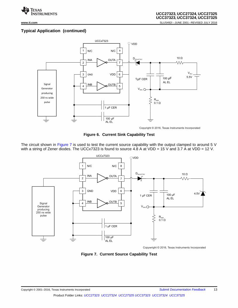
The circuit shown in Figure 7 is used to test the current source capability with the output clamped to around 5 Vwith a string of Zener diodes. The UCCx7323 is found to source 4.8 A at VDD = 15 V and 3.7 A at VDD = 12 V.
Figure 7. Current Source Capability Test
UCCx7323/4
1
2
3
4
8
7
6
5
N/C
INA
INB
GND
N/C
OUTA
OUTB
VDD
0.1�F
IN
1.0�F
RG
RG
14
UCC27323, UCC27324, UCC27325UCC37323, UCC37324, UCC37325SLUS492I –JUNE 2001–REVISED JULY 2016 www.ti.com
Product Folder Links: UCC27323 UCC27324 UCC27325 UCC37323 UCC37324 UCC37325
Submit Documentation Feedback Copyright © 2001–2016, Texas Instruments Incorporated
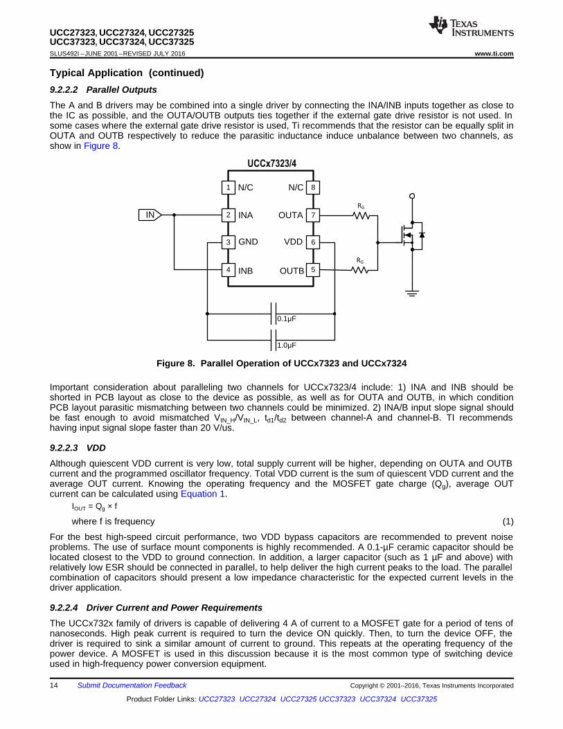
Typical Application (continued)9.2.2.2 Parallel OutputsThe A and B drivers may be combined into a single driver by connecting the INA/INB inputs together as close tothe IC as possible, and the OUTA/OUTB outputs ties together if the external gate drive resistor is not used. Insome cases where the external gate drive resistor is used, Ti recommends that the resistor can be equally split inOUTA and OUTB respectively to reduce the parasitic inductance induce unbalance between two channels, asshow in Figure 8.
Figure 8. Parallel Operation of UCCx7323 and UCCx7324
Important consideration about paralleling two channels for UCCx7323/4 include: 1) INA and INB should beshorted in PCB layout as close to the device as possible, as well as for OUTA and OUTB, in which conditionPCB layout parasitic mismatching between two channels could be minimized. 2) INA/B input slope signal shouldbe fast enough to avoid mismatched VIN_H/VIN_L, td1/td2 between channel-A and channel-B. TI recommendshaving input signal slope faster than 20 V/us.
9.2.2.3 VDDAlthough quiescent VDD current is very low, total supply current will be higher, depending on OUTA and OUTBcurrent and the programmed oscillator frequency. Total VDD current is the sum of quiescent VDD current and theaverage OUT current. Knowing the operating frequency and the MOSFET gate charge (Qg), average OUTcurrent can be calculated using Equation 1.
IOUT = Qg × f
where f is frequency (1)
For the best high-speed circuit performance, two VDD bypass capacitors are recommended to prevent noiseproblems. The use of surface mount components is highly recommended. A 0.1-µF ceramic capacitor should belocated closest to the VDD to ground connection. In addition, a larger capacitor (such as 1 µF and above) withrelatively low ESR should be connected in parallel, to help deliver the high current peaks to the load. The parallelcombination of capacitors should present a low impedance characteristic for the expected current levels in thedriver application.
9.2.2.4 Driver Current and Power RequirementsThe UCCx732x family of drivers is capable of delivering 4 A of current to a MOSFET gate for a period of tens ofnanoseconds. High peak current is required to turn the device ON quickly. Then, to turn the device OFF, thedriver is required to sink a similar amount of current to ground. This repeats at the operating frequency of thepower device. A MOSFET is used in this discussion because it is the most common type of switching deviceused in high-frequency power conversion equipment.
15
UCC27323, UCC27324, UCC27325UCC37323, UCC37324, UCC37325
www.ti.com SLUS492I –JUNE 2001–REVISED JULY 2016
Product Folder Links: UCC27323 UCC27324 UCC27325 UCC37323 UCC37324 UCC37325
Submit Documentation FeedbackCopyright © 2001–2016, Texas Instruments Incorporated
Typical Application (continued)Reference [1] and reference [2] discuss the current required to drive a power MOSFET and other capacitive-inputswitching devices. Reference [2] includes information on the previous generation of bipolar IC gate drivers.
When a driver IC is tested with a discrete, capacitive load, it is a fairly simple matter to calculate the power that isrequired from the bias supply. The energy that must be transferred from the bias supply to charge the capacitoris given by Equation 2.
E = ½CV2
where• C is the load capacitor• V is the bias voltage feeding the driver (2)
There is an equal amount of energy transferred to ground when the capacitor is discharged. This leads to apower loss given by Equation 3.
P = CV2 × f
where f is the switching frequency (3)
This power is dissipated in the resistive elements of the circuit. Thus, with no external resistor between the driverand gate, this power is dissipated inside the driver. Half of the total power is dissipated when the capacitor ischarged, and the other half is dissipated when the capacitor is discharged. An actual example using theconditions of the previous gate drive waveform should help clarify this.
With VDD = 12 V, CLOAD = 10 nF, and f = 300 kHz, the power loss can be calculated as Equation 4.P = 10 nF × (12 V)2 × (300 kHz) = 0.432 W (4)
With a 12-V supply, this equates to a current of (see Equation 5):I = P/V = 0.432 W /12 V = 36 mA (5)
The actual current measured from the supply was 0.037 A, and is very close to the predicted value. But, the IDDcurrent that is due to the IC internal consumption should be considered. With no load the IC current draw is0.0027 A. Under this condition the output rise and fall times are faster than with a load. This could lead to analmost insignificant, yet measurable current due to cross-conduction in the output stages of the driver. However,these small current differences are buried in the high frequency switching spikes, and are beyond themeasurement capabilities of a basic lab setup. The measured current with 10-nF load is reasonably close to thatexpected.
The switching load presented by a power MOSFET can be converted to an equivalent capacitance by examiningthe gate charge required to switch the device. This gate charge includes the effects of the input capacitance plusthe added charge needed to swing the drain of the device between the ON and OFF states. Most manufacturersprovide specifications that provide the typical and maximum gate charge, in nC, to switch the device underspecified conditions. Using the gate charge Qg, one can determine the power that must be dissipated whencharging a capacitor. This is done by using the equivalence Qg = Ceff × V to provide Equation 6 for power:
P = C × V2 × f = V × Qg × f (6)
Equation 6 allows a power designer to calculate the bias power required to drive a specific MOSFET gate at aspecific bias voltage and a specific switching frequency.
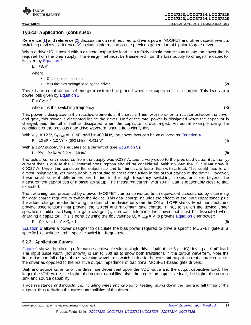
9.2.3 Application CurvesFigure 9 shows the circuit performance achievable with a single driver (half of the 8-pin IC) driving a 10-nF load.The input pulse width (not shown) is set to 300 ns to show both transitions in the output waveform. Note thelinear rise and fall edges of the switching waveforms which is due to the constant output current characteristic ofthe driver as opposed to the resistive output impedance of traditional MOSFET-based gate drivers.
Sink and source currents of the driver are dependent upon the VDD value and the output capacitive load. Thelarger the VDD value, the higher the current capability; also, the larger the capacitive load, the higher the currentsink and source capability.
Trace resistance and inductance, including wires and cables for testing, slows down the rise and fall times of theoutputs; thus reducing the current capabilities of the driver.
16
UCC27323, UCC27324, UCC27325UCC37323, UCC37324, UCC37325SLUS492I –JUNE 2001–REVISED JULY 2016 www.ti.com
Product Folder Links: UCC27323 UCC27324 UCC27325 UCC37323 UCC37324 UCC37325
Submit Documentation Feedback Copyright © 2001–2016, Texas Instruments Incorporated
Typical Application (continued)To achieve higher current results, reduce resistance and inductance on the board as much as possible andincrease the capacitive load value in order to swamp out the effect of inductance values.
CL = 10 nF, CL = 10 nF, VDD = 12 V
Figure 9. Rising and Falling Time of UCCx732x
10 Power Supply RecommendationsThe recommended bias supply voltage range for UCCx732x is from 4.5 V to 15 V. The upper end of this range isdriven by the 16 V absolute maximum voltage rating of the VDD. TI recommends keeping proper margin to allowfor transient voltage spikes.
A local bypass capacitor must be placed between the VDD and GND pins. And this capacitor must be placed asclose to the device as possible. A low ESR, ceramic surface mount capacitor is recommended. TI recommendsusing 2 capacitors across VDD and GND: a 100-nF ceramic surface-mount capacitor for high frequency filteringplaced very close to VDD and GND pin, and another surface-mount capacitor, 220 nF to10 µF, for IC bias requirements.
UCCx732x
INA
GND
INB
OUTA
VDD
OUTB
Ground plane (Bottom Layer)
Bypassing Cap, 0.1�F
Ext. Gate Resistance(Ch-A)
To Ch-A Load
Ext. Gate Resistance(Ch-B)
To Ch-B Load
Bypassing Cap, 1.0�F
17
UCC27323, UCC27324, UCC27325UCC37323, UCC37324, UCC37325
www.ti.com SLUS492I –JUNE 2001–REVISED JULY 2016
Product Folder Links: UCC27323 UCC27324 UCC27325 UCC37323 UCC37324 UCC37325
Submit Documentation FeedbackCopyright © 2001–2016, Texas Instruments Incorporated
11 Layout
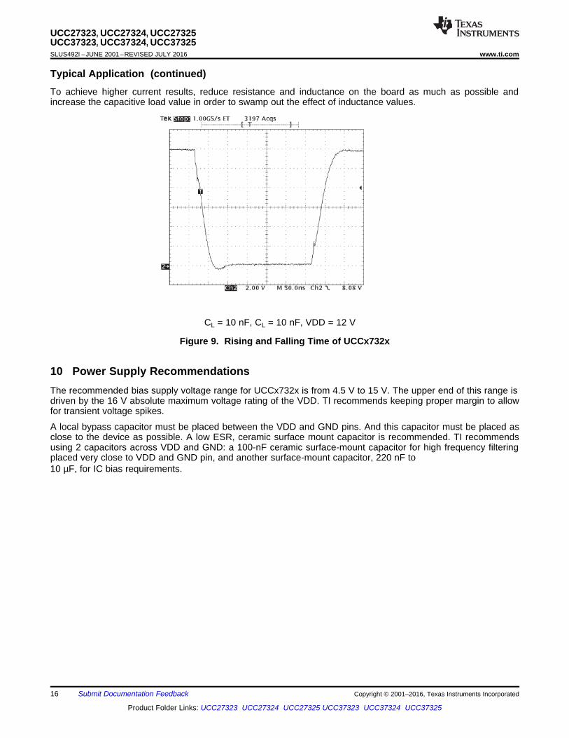
11.1 Layout GuidelinesOptimum performance of high and low-side gate drivers cannot be achieved without taking due considerationsduring circuit board layout. The following points are emphasized:
1) Low ESR/ESL capacitors must be connected close to the IC between VDD and GND pins to support highpeak currents drawn from VDD during the turn-on of the external MOSFETs.
2) Grounding considerations:The first priority in designing grounding connections is to confine the high peak currents that charge anddischarge the MOSFET gates to a minimal physical area. This will decrease the loop inductance andminimize noise issues on the gate terminals of the MOSFETs. The gate driver must be placed as close aspossible to the MOSFETs.Star-point grounding is a good way to minimize noise coupling from one current loop to another. The GND ofthe driver is connected to the other circuit nodes such as source of power MOSFET and ground of PWMcontroller at one, single point. The connected paths must be as short as possible to reduce inductance andbe as wide as possible to reduce resistance.Use a ground plane to provide noise shielding. Fast rise and fall times at OUT may corrupt the input signalsduring transition. The ground plane must not be a conduction path for any current loop. Instead the groundplane must be connected to the star-point with one single trace to establish the ground potential. In additionto noise shielding, the ground plane can help in power dissipation as well.
3) In noisy environments, tying inputs of an unused channel of the UCC2742x device to VDD or GND using shorttraces in order to ensure that the output is enabled and to prevent noise from causing malfunction in the outputmay be necessary.
4) Separate power traces and signal traces, such as output and input signals.
11.2 Layout Example
Figure 10. Recommended PCB Layout for UCCx732x
18
UCC27323, UCC27324, UCC27325UCC37323, UCC37324, UCC37325SLUS492I –JUNE 2001–REVISED JULY 2016 www.ti.com
Product Folder Links: UCC27323 UCC27324 UCC27325 UCC37323 UCC37324 UCC37325
Submit Documentation Feedback Copyright © 2001–2016, Texas Instruments Incorporated
11.3 Thermal ConsiderationsThe useful range of a driver is greatly affected by the drive power requirements of the load and the thermalcharacteristics of the IC package. In order for a power driver to be useful over a particular temperature range, thepackage must allow for the efficient removal of the heat produced while keeping the junction temperature withinrated limits. The UCCx732x family of drivers is available in three different packages to cover a range ofapplication requirements.
The MSOP PowerPAD-8 (DGN) package significantly relieves this concern by offering an effective means ofremoving the heat from the semiconductor junction. As illustrated in reference [3], the PowerPAD packages offera lead-frame die pad that is exposed at the base of the package. This pad is soldered to the copper on the PCboard directly underneath the IC package, reducing the θJC down to 4.7°C/W. Data is presented in reference [3]to show that the power dissipation can be quadrupled in the PowerPAD configuration when compared to thestandard packages. The PC board must be designed with thermal lands and thermal vias to complete the heatremoval subsystem, as summarized in reference [4]. This design allows a significant improvement in heat sinkingover that which is available in the D or P packages, and is shown to more than double the power capability of theD and P packages.
NOTEThe PowerPAD is not directly connected to any leads of the package. However, thePowerPad is electrically and thermally connected to the substrate which is the ground ofthe device.
19
UCC27323, UCC27324, UCC27325UCC37323, UCC37324, UCC37325
www.ti.com SLUS492I –JUNE 2001–REVISED JULY 2016
Product Folder Links: UCC27323 UCC27324 UCC27325 UCC37323 UCC37324 UCC37325
Submit Documentation FeedbackCopyright © 2001–2016, Texas Instruments Incorporated
12 Device and Documentation Support
12.1 Documentation Support
12.1.1 Related DocumentationSee the following for related documentation:1. Power Supply Seminar SEM-1400 Topic 2, Design And Application Guide For High Speed MOSFET Gate
Drive Circuits (SLUP133)2. Practical Considerations in High Performance MOSFET, IGBT and MCT Gate Drive Circuits (SLUA105)3. PowerPad Thermally Enhanced Package (SLMA002)4. PowerPAD Made Easy (SLMA004)
12.2 Related LinksThe table below lists quick access links. Categories include technical documents, support and communityresources, tools and software, and quick access to sample or buy.
Table 2. Related Links
PARTS PRODUCT FOLDER SAMPLE & BUY TECHNICALDOCUMENTS
TOOLS &SOFTWARE
SUPPORT &COMMUNITY
UCC27323 Click here Click here Click here Click here Click hereUCC27324 Click here Click here Click here Click here Click hereUCC27325 Click here Click here Click here Click here Click hereUCC37323 Click here Click here Click here Click here Click hereUCC37324 Click here Click here Click here Click here Click hereUCC37325 Click here Click here Click here Click here Click here
12.3 Receiving Notification of Documentation UpdatesTo receive notification of documentation updates, navigate to the device product folder on ti.com. In the upperright corner, click on Alert me to register and receive a weekly digest of any product information that haschanged. For change details, review the revision history included in any revised document.
12.4 Community ResourceThe following links connect to TI community resources. Linked contents are provided "AS IS" by the respectivecontributors. They do not constitute TI specifications and do not necessarily reflect TI's views; see TI's Terms ofUse.
TI E2E™ Online Community TI's Engineer-to-Engineer (E2E) Community. Created to foster collaborationamong engineers. At e2e.ti.com, you can ask questions, share knowledge, explore ideas and helpsolve problems with fellow engineers.
Design Support TI's Design Support Quickly find helpful E2E forums along with design support tools andcontact information for technical support.
12.5 TrademarksPowerPAD, TrueDrive, E2E are trademarks of Texas Instruments.All other trademarks are the property of their respective owners.
12.6 Electrostatic Discharge CautionThese devices have limited built-in ESD protection. The leads should be shorted together or the device placed in conductive foamduring storage or handling to prevent electrostatic damage to the MOS gates.
20
UCC27323, UCC27324, UCC27325UCC37323, UCC37324, UCC37325SLUS492I –JUNE 2001–REVISED JULY 2016 www.ti.com
Product Folder Links: UCC27323 UCC27324 UCC27325 UCC37323 UCC37324 UCC37325
Submit Documentation Feedback Copyright © 2001–2016, Texas Instruments Incorporated
12.7 GlossarySLYZ022 — TI Glossary.
This glossary lists and explains terms, acronyms, and definitions.
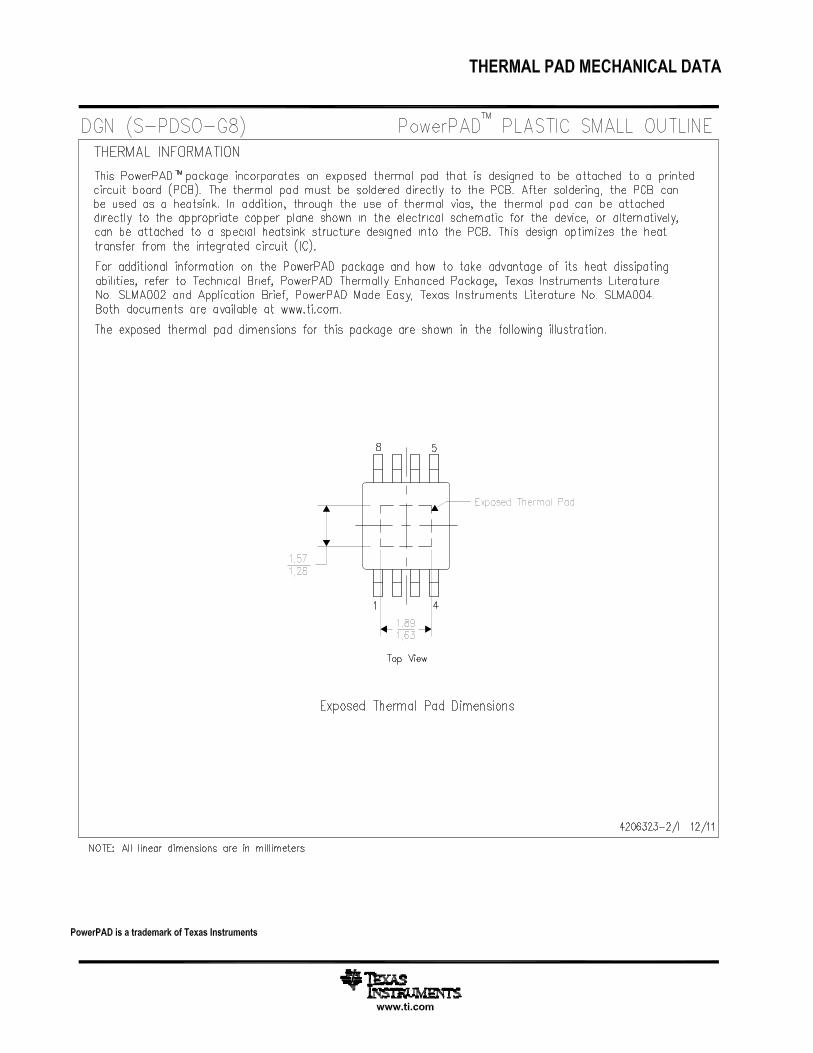
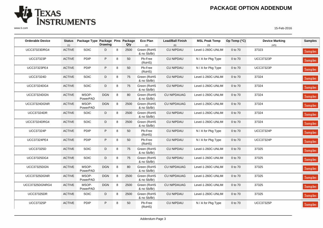
13 Mechanical, Packaging, and Orderable InformationThe following pages include mechanical, packaging, and orderable information. This information is the mostcurrent data available for the designated devices. This data is subject to change without notice and revision ofthis document. For browser-based versions of this data sheet, refer to the left-hand navigation.
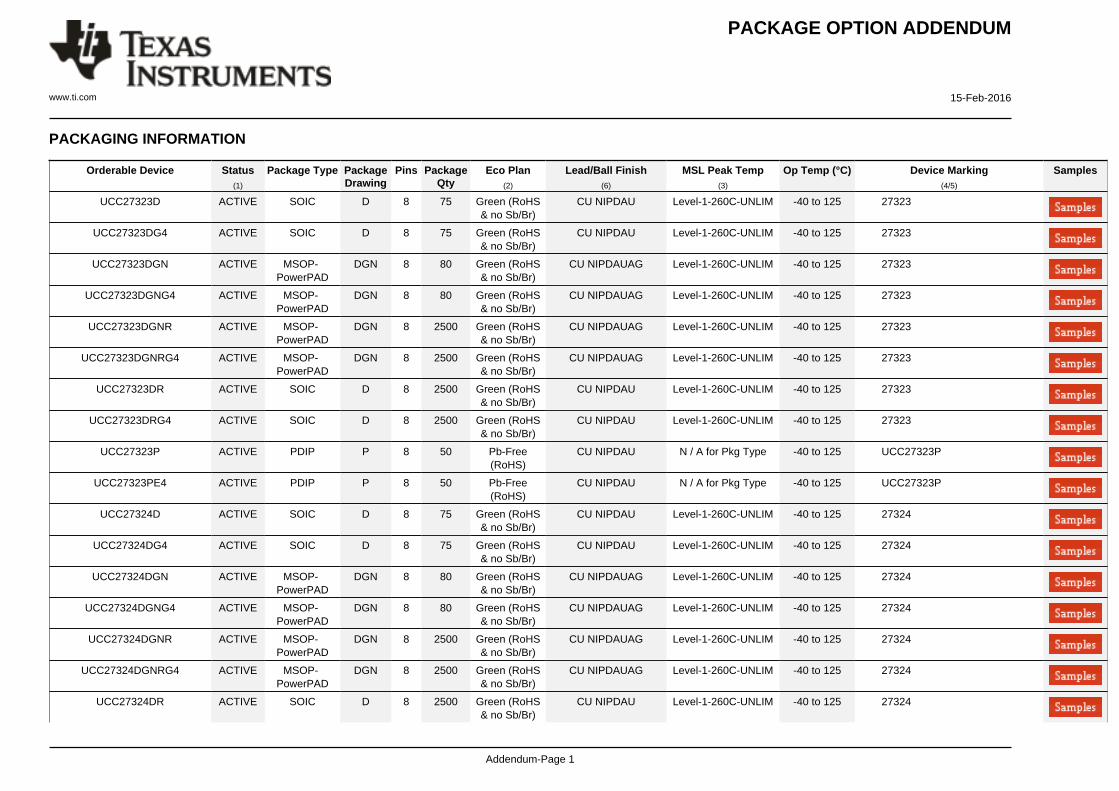
PACKAGE OPTION ADDENDUM
www.ti.com 15-Feb-2016
Addendum-Page 1
PACKAGING INFORMATION
Orderable Device Status(1)
Package Type PackageDrawing
Pins PackageQty
Eco Plan(2)
Lead/Ball Finish(6)
MSL Peak Temp(3)
Op Temp (°C) Device Marking(4/5)
Samples
UCC27323D ACTIVE SOIC D 8 75 Green (RoHS& no Sb/Br)
CU NIPDAU Level-1-260C-UNLIM -40 to 125 27323
UCC27323DG4 ACTIVE SOIC D 8 75 Green (RoHS& no Sb/Br)
CU NIPDAU Level-1-260C-UNLIM -40 to 125 27323
UCC27323DGN ACTIVE MSOP-PowerPAD
DGN 8 80 Green (RoHS& no Sb/Br)
CU NIPDAUAG Level-1-260C-UNLIM -40 to 125 27323
UCC27323DGNG4 ACTIVE MSOP-PowerPAD
DGN 8 80 Green (RoHS& no Sb/Br)
CU NIPDAUAG Level-1-260C-UNLIM -40 to 125 27323
UCC27323DGNR ACTIVE MSOP-PowerPAD
DGN 8 2500 Green (RoHS& no Sb/Br)
CU NIPDAUAG Level-1-260C-UNLIM -40 to 125 27323
UCC27323DGNRG4 ACTIVE MSOP-PowerPAD
DGN 8 2500 Green (RoHS& no Sb/Br)
CU NIPDAUAG Level-1-260C-UNLIM -40 to 125 27323
UCC27323DR ACTIVE SOIC D 8 2500 Green (RoHS& no Sb/Br)
CU NIPDAU Level-1-260C-UNLIM -40 to 125 27323
UCC27323DRG4 ACTIVE SOIC D 8 2500 Green (RoHS& no Sb/Br)
CU NIPDAU Level-1-260C-UNLIM -40 to 125 27323
UCC27323P ACTIVE PDIP P 8 50 Pb-Free(RoHS)
CU NIPDAU N / A for Pkg Type -40 to 125 UCC27323P
UCC27323PE4 ACTIVE PDIP P 8 50 Pb-Free(RoHS)
CU NIPDAU N / A for Pkg Type -40 to 125 UCC27323P
UCC27324D ACTIVE SOIC D 8 75 Green (RoHS& no Sb/Br)
CU NIPDAU Level-1-260C-UNLIM -40 to 125 27324
UCC27324DG4 ACTIVE SOIC D 8 75 Green (RoHS& no Sb/Br)
CU NIPDAU Level-1-260C-UNLIM -40 to 125 27324
UCC27324DGN ACTIVE MSOP-PowerPAD
DGN 8 80 Green (RoHS& no Sb/Br)
CU NIPDAUAG Level-1-260C-UNLIM -40 to 125 27324
UCC27324DGNG4 ACTIVE MSOP-PowerPAD
DGN 8 80 Green (RoHS& no Sb/Br)
CU NIPDAUAG Level-1-260C-UNLIM -40 to 125 27324
UCC27324DGNR ACTIVE MSOP-PowerPAD
DGN 8 2500 Green (RoHS& no Sb/Br)
CU NIPDAUAG Level-1-260C-UNLIM -40 to 125 27324
UCC27324DGNRG4 ACTIVE MSOP-PowerPAD
DGN 8 2500 Green (RoHS& no Sb/Br)
CU NIPDAUAG Level-1-260C-UNLIM -40 to 125 27324
UCC27324DR ACTIVE SOIC D 8 2500 Green (RoHS& no Sb/Br)
CU NIPDAU Level-1-260C-UNLIM -40 to 125 27324

PACKAGE OPTION ADDENDUM
www.ti.com 15-Feb-2016
Addendum-Page 2
Orderable Device Status(1)
Package Type PackageDrawing
Pins PackageQty
Eco Plan(2)
Lead/Ball Finish(6)
MSL Peak Temp(3)
Op Temp (°C) Device Marking(4/5)
Samples
UCC27324DRG4 ACTIVE SOIC D 8 2500 Green (RoHS& no Sb/Br)
CU NIPDAU Level-1-260C-UNLIM -40 to 125 27324
UCC27324P ACTIVE PDIP P 8 50 Pb-Free(RoHS)
CU NIPDAU N / A for Pkg Type -40 to 125 UCC27324P
UCC27324PE4 ACTIVE PDIP P 8 50 Pb-Free(RoHS)
CU NIPDAU N / A for Pkg Type -40 to 125 UCC27324P
UCC27325D ACTIVE SOIC D 8 75 Green (RoHS& no Sb/Br)
CU NIPDAU Level-1-260C-UNLIM -40 to 125 27325
UCC27325DG4 ACTIVE SOIC D 8 75 Green (RoHS& no Sb/Br)
CU NIPDAU Level-1-260C-UNLIM -40 to 125 27325
UCC27325DGN ACTIVE MSOP-PowerPAD
DGN 8 80 Green (RoHS& no Sb/Br)
CU NIPDAUAG Level-1-260C-UNLIM -40 to 125 27325
UCC27325DGNG4 ACTIVE MSOP-PowerPAD
DGN 8 80 Green (RoHS& no Sb/Br)
CU NIPDAUAG Level-1-260C-UNLIM -40 to 125 27325
UCC27325DGNR ACTIVE MSOP-PowerPAD
DGN 8 2500 Green (RoHS& no Sb/Br)
CU NIPDAUAG Level-1-260C-UNLIM -40 to 125 27325
UCC27325DR ACTIVE SOIC D 8 2500 Green (RoHS& no Sb/Br)
CU NIPDAU Level-1-260C-UNLIM -40 to 125 27325
UCC27325P ACTIVE PDIP P 8 50 Pb-Free(RoHS)
CU NIPDAU N / A for Pkg Type -40 to 125 UCC27325P
UCC27325PE4 ACTIVE PDIP P 8 50 Pb-Free(RoHS)
CU NIPDAU N / A for Pkg Type -40 to 125 UCC27325P
UCC37323D ACTIVE SOIC D 8 75 Green (RoHS& no Sb/Br)
CU NIPDAU Level-1-260C-UNLIM 0 to 70 37323
UCC37323DG4 ACTIVE SOIC D 8 75 Green (RoHS& no Sb/Br)
CU NIPDAU Level-1-260C-UNLIM 0 to 70 37323
UCC37323DGN ACTIVE MSOP-PowerPAD
DGN 8 80 Green (RoHS& no Sb/Br)
CU NIPDAUAG Level-1-260C-UNLIM 0 to 70 37323
UCC37323DGNG4 ACTIVE MSOP-PowerPAD
DGN 8 80 Green (RoHS& no Sb/Br)
CU NIPDAUAG Level-1-260C-UNLIM 0 to 70 37323
UCC37323DGNR ACTIVE MSOP-PowerPAD
DGN 8 2500 Green (RoHS& no Sb/Br)
CU NIPDAUAG Level-1-260C-UNLIM 0 to 70 37323
UCC37323DGNRG4 ACTIVE MSOP-PowerPAD
DGN 8 2500 Green (RoHS& no Sb/Br)
CU NIPDAUAG Level-1-260C-UNLIM 0 to 70 37323
UCC37323DR ACTIVE SOIC D 8 2500 Green (RoHS& no Sb/Br)
CU NIPDAU Level-1-260C-UNLIM 0 to 70 37323
PACKAGE OPTION ADDENDUM
www.ti.com 15-Feb-2016
Addendum-Page 3
Orderable Device Status(1)
Package Type PackageDrawing
Pins PackageQty
Eco Plan(2)
Lead/Ball Finish(6)
MSL Peak Temp(3)
Op Temp (°C) Device Marking(4/5)
Samples
UCC37323DRG4 ACTIVE SOIC D 8 2500 Green (RoHS& no Sb/Br)
CU NIPDAU Level-1-260C-UNLIM 0 to 70 37323
UCC37323P ACTIVE PDIP P 8 50 Pb-Free(RoHS)
CU NIPDAU N / A for Pkg Type 0 to 70 UCC37323P
UCC37323PE4 ACTIVE PDIP P 8 50 Pb-Free(RoHS)
CU NIPDAU N / A for Pkg Type 0 to 70 UCC37323P
UCC37324D ACTIVE SOIC D 8 75 Green (RoHS& no Sb/Br)
CU NIPDAU Level-1-260C-UNLIM 0 to 70 37324
UCC37324DG4 ACTIVE SOIC D 8 75 Green (RoHS& no Sb/Br)
CU NIPDAU Level-1-260C-UNLIM 0 to 70 37324
UCC37324DGN ACTIVE MSOP-PowerPAD
DGN 8 80 Green (RoHS& no Sb/Br)
CU NIPDAUAG Level-1-260C-UNLIM 0 to 70 37324
UCC37324DGNR ACTIVE MSOP-PowerPAD
DGN 8 2500 Green (RoHS& no Sb/Br)
CU NIPDAUAG Level-1-260C-UNLIM 0 to 70 37324
UCC37324DR ACTIVE SOIC D 8 2500 Green (RoHS& no Sb/Br)
CU NIPDAU Level-1-260C-UNLIM 0 to 70 37324
UCC37324DRG4 ACTIVE SOIC D 8 2500 Green (RoHS& no Sb/Br)
CU NIPDAU Level-1-260C-UNLIM 0 to 70 37324
UCC37324P ACTIVE PDIP P 8 50 Pb-Free(RoHS)
CU NIPDAU N / A for Pkg Type 0 to 70 UCC37324P
UCC37324PE4 ACTIVE PDIP P 8 50 Pb-Free(RoHS)
CU NIPDAU N / A for Pkg Type 0 to 70 UCC37324P
UCC37325D ACTIVE SOIC D 8 75 Green (RoHS& no Sb/Br)
CU NIPDAU Level-1-260C-UNLIM 0 to 70 37325
UCC37325DG4 ACTIVE SOIC D 8 75 Green (RoHS& no Sb/Br)
CU NIPDAU Level-1-260C-UNLIM 0 to 70 37325
UCC37325DGN ACTIVE MSOP-PowerPAD
DGN 8 80 Green (RoHS& no Sb/Br)
CU NIPDAUAG Level-1-260C-UNLIM 0 to 70 37325
UCC37325DGNR ACTIVE MSOP-PowerPAD
DGN 8 2500 Green (RoHS& no Sb/Br)
CU NIPDAUAG Level-1-260C-UNLIM 0 to 70 37325
UCC37325DGNRG4 ACTIVE MSOP-PowerPAD
DGN 8 2500 Green (RoHS& no Sb/Br)
CU NIPDAUAG Level-1-260C-UNLIM 0 to 70 37325
UCC37325DR ACTIVE SOIC D 8 2500 Green (RoHS& no Sb/Br)
CU NIPDAU Level-1-260C-UNLIM 0 to 70 37325
UCC37325P ACTIVE PDIP P 8 50 Pb-Free(RoHS)
CU NIPDAU N / A for Pkg Type 0 to 70 UCC37325P
PACKAGE OPTION ADDENDUM
www.ti.com 15-Feb-2016
Addendum-Page 4
Orderable Device Status(1)
Package Type PackageDrawing
Pins PackageQty
Eco Plan(2)
Lead/Ball Finish(6)
MSL Peak Temp(3)
Op Temp (°C) Device Marking(4/5)
Samples
UCC37325PE4 ACTIVE PDIP P 8 50 Pb-Free(RoHS)
CU NIPDAU N / A for Pkg Type 0 to 70 UCC37325P
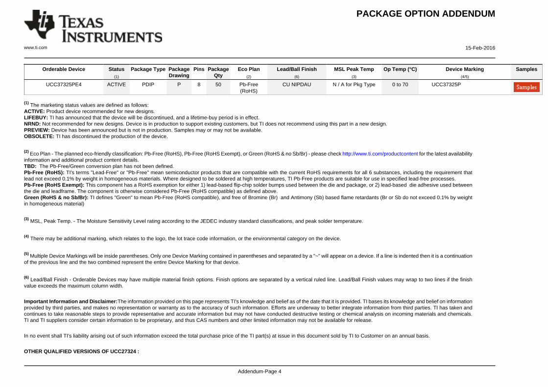
(1) The marketing status values are defined as follows:ACTIVE: Product device recommended for new designs.LIFEBUY: TI has announced that the device will be discontinued, and a lifetime-buy period is in effect.NRND: Not recommended for new designs. Device is in production to support existing customers, but TI does not recommend using this part in a new design.PREVIEW: Device has been announced but is not in production. Samples may or may not be available.OBSOLETE: TI has discontinued the production of the device.
(2) Eco Plan - The planned eco-friendly classification: Pb-Free (RoHS), Pb-Free (RoHS Exempt), or Green (RoHS & no Sb/Br) - please check http://www.ti.com/productcontent for the latest availabilityinformation and additional product content details.TBD: The Pb-Free/Green conversion plan has not been defined.Pb-Free (RoHS): TI's terms "Lead-Free" or "Pb-Free" mean semiconductor products that are compatible with the current RoHS requirements for all 6 substances, including the requirement thatlead not exceed 0.1% by weight in homogeneous materials. Where designed to be soldered at high temperatures, TI Pb-Free products are suitable for use in specified lead-free processes.Pb-Free (RoHS Exempt): This component has a RoHS exemption for either 1) lead-based flip-chip solder bumps used between the die and package, or 2) lead-based die adhesive used betweenthe die and leadframe. The component is otherwise considered Pb-Free (RoHS compatible) as defined above.Green (RoHS & no Sb/Br): TI defines "Green" to mean Pb-Free (RoHS compatible), and free of Bromine (Br) and Antimony (Sb) based flame retardants (Br or Sb do not exceed 0.1% by weightin homogeneous material)
(3) MSL, Peak Temp. - The Moisture Sensitivity Level rating according to the JEDEC industry standard classifications, and peak solder temperature.
(4) There may be additional marking, which relates to the logo, the lot trace code information, or the environmental category on the device.
(5) Multiple Device Markings will be inside parentheses. Only one Device Marking contained in parentheses and separated by a "~" will appear on a device. If a line is indented then it is a continuationof the previous line and the two combined represent the entire Device Marking for that device.
(6) Lead/Ball Finish - Orderable Devices may have multiple material finish options. Finish options are separated by a vertical ruled line. Lead/Ball Finish values may wrap to two lines if the finishvalue exceeds the maximum column width.
Important Information and Disclaimer:The information provided on this page represents TI's knowledge and belief as of the date that it is provided. TI bases its knowledge and belief on informationprovided by third parties, and makes no representation or warranty as to the accuracy of such information. Efforts are underway to better integrate information from third parties. TI has taken andcontinues to take reasonable steps to provide representative and accurate information but may not have conducted destructive testing or chemical analysis on incoming materials and chemicals.TI and TI suppliers consider certain information to be proprietary, and thus CAS numbers and other limited information may not be available for release.
In no event shall TI's liability arising out of such information exceed the total purchase price of the TI part(s) at issue in this document sold by TI to Customer on an annual basis.
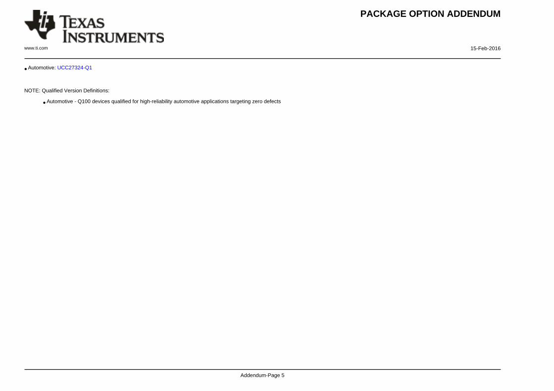
OTHER QUALIFIED VERSIONS OF UCC27324 :
PACKAGE OPTION ADDENDUM
www.ti.com 15-Feb-2016
Addendum-Page 5
• Automotive: UCC27324-Q1
NOTE: Qualified Version Definitions:
• Automotive - Q100 devices qualified for high-reliability automotive applications targeting zero defects
TAPE AND REEL INFORMATION
*All dimensions are nominal
Device PackageType
PackageDrawing
Pins SPQ ReelDiameter
(mm)
ReelWidth
W1 (mm)
A0(mm)
B0(mm)
K0(mm)
P1(mm)
W(mm)
Pin1Quadrant
UCC27323DGNR MSOP-Power PAD
DGN 8 2500 330.0 12.4 5.3 3.4 1.4 8.0 12.0 Q1
UCC27323DR SOIC D 8 2500 330.0 12.4 6.4 5.2 2.1 8.0 12.0 Q1
UCC27324DGNR MSOP-Power PAD
DGN 8 2500 330.0 12.4 5.3 3.4 1.4 8.0 12.0 Q1
UCC27324DR SOIC D 8 2500 330.0 12.4 6.4 5.2 2.1 8.0 12.0 Q1
UCC27324DR SOIC D 8 2500 330.0 12.4 6.4 5.2 2.1 8.0 12.0 Q1
UCC27325DGNR MSOP-Power PAD
DGN 8 2500 330.0 12.4 5.3 3.4 1.4 8.0 12.0 Q1
UCC27325DR SOIC D 8 2500 330.0 12.4 6.4 5.2 2.1 8.0 12.0 Q1
UCC37323DGNR MSOP-Power PAD
DGN 8 2500 330.0 12.4 5.3 3.4 1.4 8.0 12.0 Q1
UCC37323DR SOIC D 8 2500 330.0 12.4 6.4 5.2 2.1 8.0 12.0 Q1
UCC37324DGNR MSOP-Power PAD
DGN 8 2500 330.0 12.4 5.3 3.4 1.4 8.0 12.0 Q1
UCC37324DR SOIC D 8 2500 330.0 12.4 6.4 5.2 2.1 8.0 12.0 Q1
PACKAGE MATERIALS INFORMATION
www.ti.com 29-Feb-2016
Pack Materials-Page 1
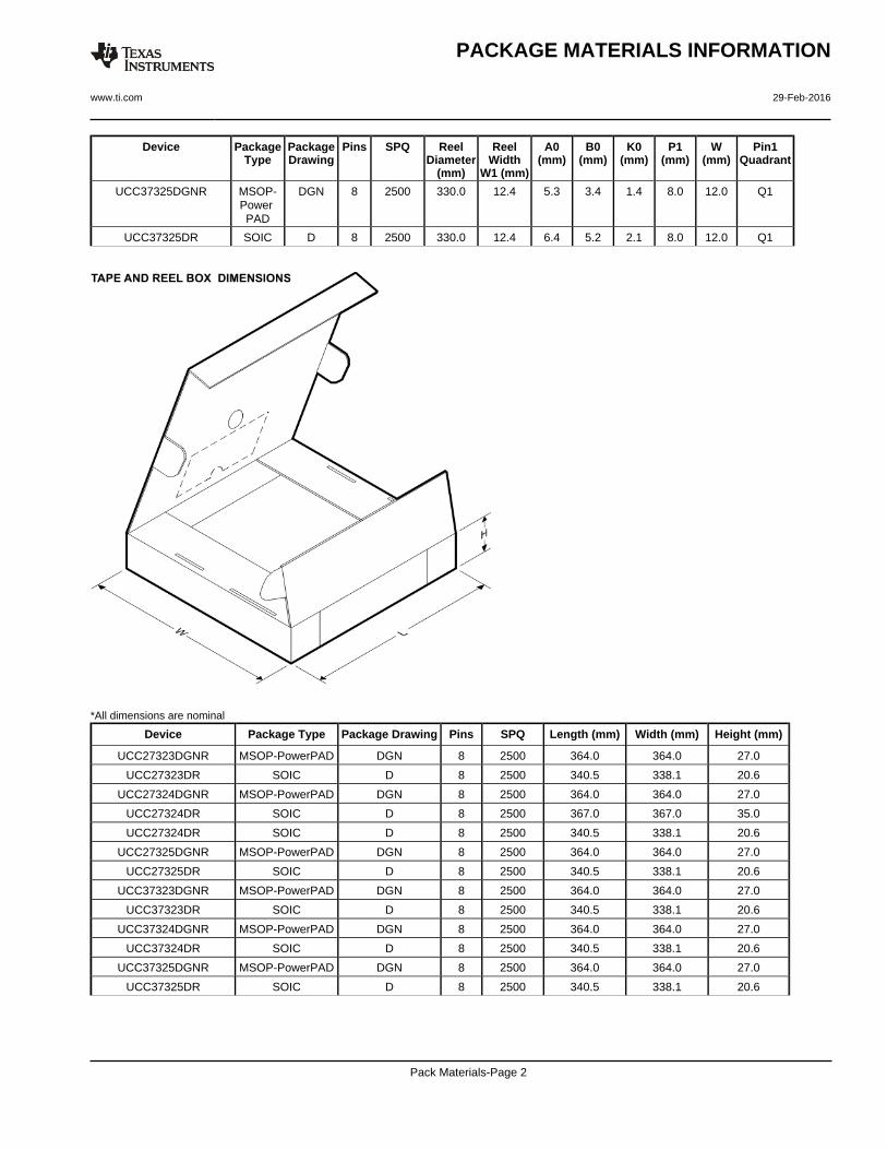
Device PackageType
PackageDrawing
Pins SPQ ReelDiameter
(mm)
ReelWidth
W1 (mm)
A0(mm)
B0(mm)
K0(mm)
P1(mm)
W(mm)
Pin1Quadrant
UCC37325DGNR MSOP-Power PAD
DGN 8 2500 330.0 12.4 5.3 3.4 1.4 8.0 12.0 Q1
UCC37325DR SOIC D 8 2500 330.0 12.4 6.4 5.2 2.1 8.0 12.0 Q1
*All dimensions are nominal
Device Package Type Package Drawing Pins SPQ Length (mm) Width (mm) Height (mm)
UCC27323DGNR MSOP-PowerPAD DGN 8 2500 364.0 364.0 27.0
UCC27323DR SOIC D 8 2500 340.5 338.1 20.6
UCC27324DGNR MSOP-PowerPAD DGN 8 2500 364.0 364.0 27.0
UCC27324DR SOIC D 8 2500 367.0 367.0 35.0
UCC27324DR SOIC D 8 2500 340.5 338.1 20.6
UCC27325DGNR MSOP-PowerPAD DGN 8 2500 364.0 364.0 27.0
UCC27325DR SOIC D 8 2500 340.5 338.1 20.6
UCC37323DGNR MSOP-PowerPAD DGN 8 2500 364.0 364.0 27.0
UCC37323DR SOIC D 8 2500 340.5 338.1 20.6
UCC37324DGNR MSOP-PowerPAD DGN 8 2500 364.0 364.0 27.0
UCC37324DR SOIC D 8 2500 340.5 338.1 20.6
UCC37325DGNR MSOP-PowerPAD DGN 8 2500 364.0 364.0 27.0
UCC37325DR SOIC D 8 2500 340.5 338.1 20.6
PACKAGE MATERIALS INFORMATION
www.ti.com 29-Feb-2016
Pack Materials-Page 2
IMPORTANT NOTICE
Texas Instruments Incorporated and its subsidiaries (TI) reserve the right to make corrections, enhancements, improvements and otherchanges to its semiconductor products and services per JESD46, latest issue, and to discontinue any product or service per JESD48, latestissue. Buyers should obtain the latest relevant information before placing orders and should verify that such information is current andcomplete. All semiconductor products (also referred to herein as “components”) are sold subject to TI’s terms and conditions of salesupplied at the time of order acknowledgment.TI warrants performance of its components to the specifications applicable at the time of sale, in accordance with the warranty in TI’s termsand conditions of sale of semiconductor products. Testing and other quality control techniques are used to the extent TI deems necessaryto support this warranty. Except where mandated by applicable law, testing of all parameters of each component is not necessarilyperformed.TI assumes no liability for applications assistance or the design of Buyers’ products. Buyers are responsible for their products andapplications using TI components. To minimize the risks associated with Buyers’ products and applications, Buyers should provideadequate design and operating safeguards.TI does not warrant or represent that any license, either express or implied, is granted under any patent right, copyright, mask work right, orother intellectual property right relating to any combination, machine, or process in which TI components or services are used. Informationpublished by TI regarding third-party products or services does not constitute a license to use such products or services or a warranty orendorsement thereof. Use of such information may require a license from a third party under the patents or other intellectual property of thethird party, or a license from TI under the patents or other intellectual property of TI.Reproduction of significant portions of TI information in TI data books or data sheets is permissible only if reproduction is without alterationand is accompanied by all associated warranties, conditions, limitations, and notices. TI is not responsible or liable for such altereddocumentation. Information of third parties may be subject to additional restrictions.Resale of TI components or services with statements different from or beyond the parameters stated by TI for that component or servicevoids all express and any implied warranties for the associated TI component or service and is an unfair and deceptive business practice.TI is not responsible or liable for any such statements.Buyer acknowledges and agrees that it is solely responsible for compliance with all legal, regulatory and safety-related requirementsconcerning its products, and any use of TI components in its applications, notwithstanding any applications-related information or supportthat may be provided by TI. Buyer represents and agrees that it has all the necessary expertise to create and implement safeguards whichanticipate dangerous consequences of failures, monitor failures and their consequences, lessen the likelihood of failures that might causeharm and take appropriate remedial actions. Buyer will fully indemnify TI and its representatives against any damages arising out of the useof any TI components in safety-critical applications.In some cases, TI components may be promoted specifically to facilitate safety-related applications. With such components, TI’s goal is tohelp enable customers to design and create their own end-product solutions that meet applicable functional safety standards andrequirements. Nonetheless, such components are subject to these terms.No TI components are authorized for use in FDA Class III (or similar life-critical medical equipment) unless authorized officers of the partieshave executed a special agreement specifically governing such use.Only those TI components which TI has specifically designated as military grade or “enhanced plastic” are designed and intended for use inmilitary/aerospace applications or environments. Buyer acknowledges and agrees that any military or aerospace use of TI componentswhich have not been so designated is solely at the Buyer's risk, and that Buyer is solely responsible for compliance with all legal andregulatory requirements in connection with such use.TI has specifically designated certain components as meeting ISO/TS16949 requirements, mainly for automotive use. In any case of use ofnon-designated products, TI will not be responsible for any failure to meet ISO/TS16949.
Products ApplicationsAudio www.ti.com/audio Automotive and Transportation www.ti.com/automotiveAmplifiers amplifier.ti.com Communications and Telecom www.ti.com/communicationsData Converters dataconverter.ti.com Computers and Peripherals www.ti.com/computersDLP® Products www.dlp.com Consumer Electronics www.ti.com/consumer-appsDSP dsp.ti.com Energy and Lighting www.ti.com/energyClocks and Timers www.ti.com/clocks Industrial www.ti.com/industrialInterface interface.ti.com Medical www.ti.com/medicalLogic logic.ti.com Security www.ti.com/securityPower Mgmt power.ti.com Space, Avionics and Defense www.ti.com/space-avionics-defenseMicrocontrollers microcontroller.ti.com Video and Imaging www.ti.com/videoRFID www.ti-rfid.comOMAP Applications Processors www.ti.com/omap TI E2E Community e2e.ti.comWireless Connectivity www.ti.com/wirelessconnectivity
Mailing Address: Texas Instruments, Post Office Box 655303, Dallas, Texas 75265Copyright © 2016, Texas Instruments Incorporated