DR ISR 1 8 DRA N - Diodes Incorporated CC)*t ONP =5V*5μs, the minimum on time is about 1.8μs. The...
10
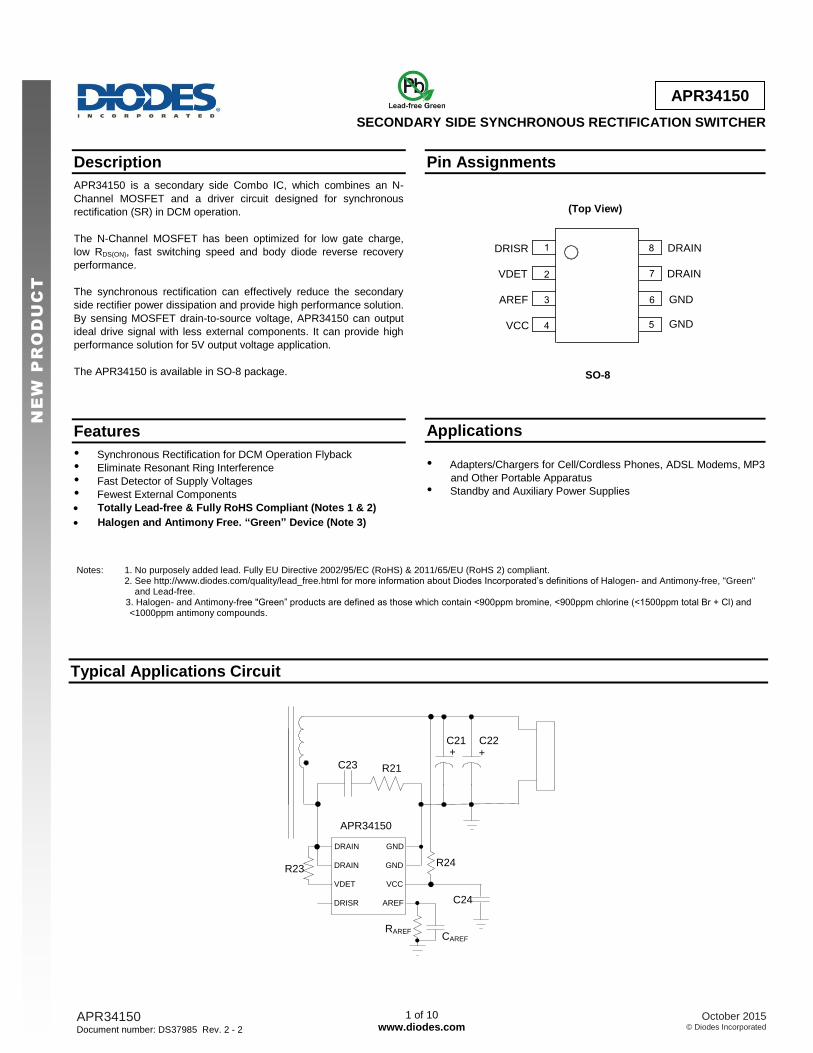
APR34150 Document number: DS37985 Rev. 2 - 2 1 of 10 www.diodes.com October 2015 © Diodes Incorporated APR34150 NEW PRODUCT SECONDARY SIDE SYNCHRONOUS RECTIFICATION SWITCHER Description APR34150 is a secondary side Combo IC, which combines an N- Channel MOSFET and a driver circuit designed for synchronous rectification (SR) in DCM operation. The N-Channel MOSFET has been optimized for low gate charge, low RDS(ON), fast switching speed and body diode reverse recovery performance. The synchronous rectification can effectively reduce the secondary side rectifier power dissipation and provide high performance solution. By sensing MOSFET drain-to-source voltage, APR34150 can output ideal drive signal with less external components. It can provide high performance solution for 5V output voltage application. The APR34150 is available in SO-8 package. Features • Synchronous Rectification for DCM Operation Flyback • Eliminate Resonant Ring Interference • Fast Detector of Supply Voltages • Fewest External Components Totally Lead-free & Fully RoHS Compliant (Notes 1 & 2) Halogen and Antimony Free. “Green” Device (Note 3) Pin Assignments (Top View) 1 2 3 4 8 7 6 5 DRISR VDET AREF VCC DRAIN DRAIN GND GND SO-8 Applications • Adapters/Chargers for Cell/Cordless Phones, ADSL Modems, MP3 and Other Portable Apparatus • Standby and Auxiliary Power Supplies Notes: 1. No purposely added lead. Fully EU Directive 2002/95/EC (RoHS) & 2011/65/EU (RoHS 2) compliant. 2. See http://www.diodes.com/quality/lead_free.html for more information about Diodes Incorporated’s definitions of Halogen- and Antimony-free, "Green" and Lead-free. 3. Halogen- and Antimony-free "Green” products are defined as those which contain <900ppm bromine, <900ppm chlorine (<1500ppm total Br + Cl) and <1000ppm antimony compounds. Typical Applications Circuit + C21 + C22 APR34150 R24 VCC AREF DRAIN DRAIN GND GND VDET DRISR R AREF C23 R21 C24 R23 C AREF
Transcript of DR ISR 1 8 DRA N - Diodes Incorporated CC)*t ONP =5V*5μs, the minimum on time is about 1.8μs. The...
APR34150 Document number: DS37985 Rev. 2 - 2
1 of 10 www.diodes.com
October 2015 © Diodes Incorporated
APR34150
NE
W P
RO
DU
CT
SECONDARY SIDE SYNCHRONOUS RECTIFICATION SWITCHER
Description
APR34150 is a secondary side Combo IC, which combines an N-
Channel MOSFET and a driver circuit designed for synchronous
rectification (SR) in DCM operation.
The N-Channel MOSFET has been optimized for low gate charge,
low RDS(ON), fast switching speed and body diode reverse recovery
performance.
The synchronous rectification can effectively reduce the secondary
side rectifier power dissipation and provide high performance solution.
By sensing MOSFET drain-to-source voltage, APR34150 can output
ideal drive signal with less external components. It can provide high
performance solution for 5V output voltage application.
The APR34150 is available in SO-8 package.
Features
• Synchronous Rectification for DCM Operation Flyback
• Eliminate Resonant Ring Interference
• Fast Detector of Supply Voltages
• Fewest External Components
Totally Lead-free & Fully RoHS Compliant (Notes 1 & 2)
Halogen and Antimony Free. “Green” Device (Note 3)
Pin Assignments
(Top View)
1
2
3
4
8
7
6
5
DRISR
VDET
AREF
VCC
DRAIN
DRAIN
GND
GND
SO-8
Applications
• Adapters/Chargers for Cell/Cordless Phones, ADSL Modems, MP3
and Other Portable Apparatus
• Standby and Auxiliary Power Supplies
Notes: 1. No purposely added lead. Fully EU Directive 2002/95/EC (RoHS) & 2011/65/EU (RoHS 2) compliant. 2. See http://www.diodes.com/quality/lead_free.html for more information about Diodes Incorporated’s definitions of Halogen- and Antimony-free, "Green" and Lead-free. 3. Halogen- and Antimony-free "Green” products are defined as those which contain <900ppm bromine, <900ppm chlorine (<1500ppm total Br + Cl) and <1000ppm antimony compounds.
Typical Applications Circuit
+C21
+C22
APR34150
R24
VCC
AREF
DRAIN
DRAIN
GND
GND
VDET
DRISR
RAREF
C23 R21
C24
R23
CAREF
APR34150 Document number: DS37985 Rev. 2 - 2
2 of 10 www.diodes.com
October 2015 © Diodes Incorporated
APR34150
NE
W P
RO
DU
CT
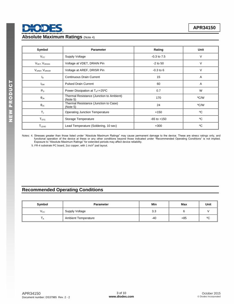
Pin Descriptions
Pin Number Pin Name Function
1 DRISR Synchronous rectification MOSFET drive
2 VDET Synchronous rectification sense input, connected to DRAIN through a resistor
3 AREF Program a voltage reference with a resistor from AREF to GND, to enable synchronous rectification MOSFET drive signal
4 VCC Power supply, connected with system output
5, 6 GND Source pin of internal MOSFET, connected to Ground
7, 8 DRAIN Drain pin of internal MOSFET
Functional Block Diagram
VREF
CountertONPDET
OSC
Integrator
(VDET-VCC)*tONP
SRDRIVER
OVP
IOVP
VD
ET
IAREF
GND
VDET
VCC
AREF
DRISR
DRAIN
1
2
3
4
7, 8
5, 6
APR34150 Document number: DS37985 Rev. 2 - 2
3 of 10 www.diodes.com
October 2015 © Diodes Incorporated
APR34150
NE
W P
RO
DU
CT
Absolute Maximum Ratings (Note 4)
Symbol Parameter Rating Unit
VCC Supply Voltage -0.3 to 7.5 V
VDET, VDRAIN Voltage at VDET, DRAIN Pin -2 to 50 V
VAREF, VDRISR Voltage at AREF, DRISR Pin -0.3 to 6 V
ID Continuous Drain Current 15 A
IDM Pulsed Drain Current 60 A
PD Power Dissipation at TA=+25ºC 0.7 W
θJA Thermal Resistance (Junction to Ambient) (Note 5)
170 ºC/W
θJC Thermal Resistance (Junction to Case) (Note 5)
24 ºC/W
TJ Operating Junction Temperature +150 ºC
TSTG Storage Temperature -65 to +150 ºC
TLEAD Lead Temperature (Soldering, 10 sec) +300 ºC
Notes: 4. Stresses greater than those listed under “Absolute Maximum Ratings” may cause permanent damage to the device. These are stress ratings only, and
functional operation of the device at these or any other conditions beyond those indicated under “Recommended Operating Conditions” is not implied. Exposure to “Absolute Maximum Ratings” for extended periods may affect device reliability.
5. FR-4 substrate PC board, 2oz copper, with 1 inch2 pad layout.
Recommended Operating Conditions
Symbol Parameter Min Max Unit
VCC Supply Voltage 3.3 6 V
TA Ambient Temperature -40 +85 ºC
APR34150 Document number: DS37985 Rev. 2 - 2
4 of 10 www.diodes.com
October 2015 © Diodes Incorporated
APR34150
NE
W P
RO
DU
CT
Electrical Characteristics (@TA = +25°C, VCC =5V, unless otherwise specified.)
Symbol Parameter Conditions Min Typ Max Unit
Supply Voltage ( VCC Pin )
ISTARTUP Startup Current VCC=VSTARTUP-0.1V – 100 150 μA
IOP Operating Current VDET pin floating VCC=VTRIGGER+20mV
40 100 150 μA
VSTARTUP Startup Voltage – – 3.1 – V
– UVLO – – 2.8 – V
VOVP Overshoot Voltage for Discharge – 5.7 5.8 5.9 V
IOVP Overshoot Current for Discharge VCC=VOVP+0.1V, VCC pin is connected to a 20Ω resistor
40 – 100 mA
Synchronous Voltage Detect
VTHON Gate Turn On Threshold – 0 – 1 V
VTHOFF Gate Turn Off Threshold – -20 -12.5 -5 mV
tDON Turn On Delay Time From VTHON to VDRISR=1V – 70 130 ns
tDOFF Turn Off Propagation Delay Time From VTHOFF to VDRISR=3V – 100 150 ns
tRG Gate Turn On Rising Time From 1V to 3V, CL=4.7nF – 50 100 ns
tFG Gate Turn Off Falling Time From 3V to 1V, CL=4.7nF – 50 100 ns
tLEB_S Minimum On Time
– 0.9 1.8 2.7 μs
tLEB_L – – – 6.5
VDRISR_HIGH Drive Output Voltage VCC=5V 3.7 – – V
VS_MIN SR Minimum Operating Voltage (Note 6)
– – – 4.5 V
tOVP_LAST Added OVP Discharge Time – – 1.0 – ms
Kqs (Note 7) (VDET-VCC)*tONP = 25Vµs 0.325 – 0.515 mA*μs
Notes: 6. This item specifies the minimum SR operating voltage of VIN_DC, VIN_DC≥NPS*VS_MIN.
7. This item is used to specify the value of RAREF.
APR34150 Document number: DS37985 Rev. 2 - 2
5 of 10 www.diodes.com
October 2015 © Diodes Incorporated
APR34150
NE
W P
RO
DU
CT
Electrical Characteristics (@TA =+25°C, unless otherwise specified. Cont.)
MOSFET Static Characteristics
Parameters Symbol Conditions Min Typ Max Unit
Drain to Source Breakdown Voltage
VDSS(BR) VGS=0V, ID=0.25mA 50 – – V
Gate Threshold Voltage VGS(TH) VDS=VGS, ID=0.25mA 0.5 0.9 2 V
Zero Gate Voltage Drain Current
IDSS VDS=50V, VGS=0V – – 1 μA
Gate to Source Leakage Current
IGSS VGS=10V, VDS=0V – – ±10 μA
Drain to Source On-state Resistance
RDS(ON) VGS=4.5V, ID=15A 12 17 30 mΩ
MOSFET Dynamic Characteristics
Parameters Symbol Conditions Min Typ Max Unit
Input Capacitance Ciss
VGS=0V, VDS=25V, f=1MHz
– 1316 –
pF Output Capacitance Coss – 97 –
Reverse Transfer Capacitance Crss – 85 –
Gate to Source Charge Qgs
VGS=0V to 10V, VDD=25V, ID=15A
– 3.2 –
nC Gate to Drain Charge (Miller Charger)
Qgd – 5.7 –
Total Gate Charge Qg – 15.2 –
Gate Resistance Rg – – 0.85 – Ω
Operation Description
MOSFET Driver
The operation of the SR is described with timing diagram shown in Figure 1. APR34150 monitors the MOSFET drain-source voltage. When the
drain voltage is lower than the turn-on threshold voltage VTHON, the IC outputs a positive drive voltage after a turn-on delay time (tDON). The
MOSFET will turn on and the current will transfer from the body diode into the MOSFET’s channel.
In the process of drain current decreasing linearly toward zero, the drain-source voltage rises synchronically. When it rises over the turn off
threshold voltage VTHOFF, APR34150 pulls the drive signal down after a turn off delay (tDOFF).
I, V
t
t
IS
VDET
VDRISR
VTHON
VTHOFF
0.1VDRISR
0.9VDRISR
0.1VDRISR
0.9VDRISR
tRGtDONtFGtDOFF
0
0
Figure 1. Typical Waveforms of APR34150
APR34150 Document number: DS37985 Rev. 2 - 2
6 of 10 www.diodes.com
October 2015 © Diodes Incorporated
APR34150
NE
W P
RO
DU
CT
Operation Description (Cont.)
Minimum On Time
When the controlled MOSFET gate is turned on, some ringing noise is generated. The minimum on-time timer blanks the VTHOFF comparator,
keeping the controlled MOSFET on for at least the minimum on time. If VTHOFF falls below the threshold before minimum on time expires, the
MOSFET will keep on until the end of the minimum on time.
The minimum on time is in direct proportion to the (VDET-VCC)*tONP. When (VDET-VCC)*tONP=5V*5μs, the minimum on time is about 1.8μs.
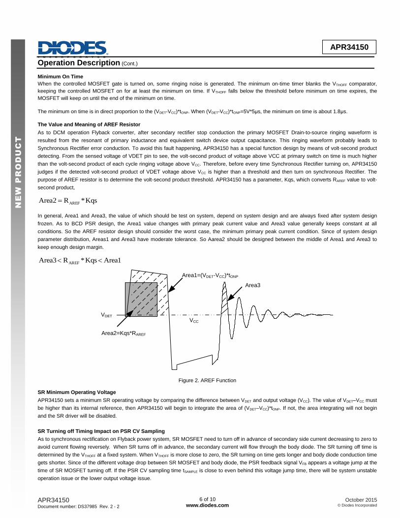
The Value and Meaning of AREF Resistor
As to DCM operation Flyback converter, after secondary rectifier stop conduction the primary MOSFET Drain-to-source ringing waveform is
resulted from the resonant of primary inductance and equivalent switch device output capacitance. This ringing waveform probably leads to
Synchronous Rectifier error conduction. To avoid this fault happening, APR34150 has a special function design by means of volt-second product
detecting. From the sensed voltage of VDET pin to see, the volt-second product of voltage above VCC at primary switch on time is much higher
than the volt-second product of each cycle ringing voltage above VCC. Therefore, before every time Synchronous Rectifier turning on, APR34150
judges if the detected volt-second product of VDET voltage above VCC is higher than a threshold and then turn on synchronous Rectifier. The
purpose of AREF resistor is to determine the volt-second product threshold. APR34150 has a parameter, Kqs, which converts RAREF value to volt-
second product,
Kqs*R2Area AREF
In general, Area1 and Area3, the value of which should be test on system, depend on system design and are always fixed after system design
frozen. As to BCD PSR design, the Area1 value changes with primary peak current value and Area3 value generally keeps constant at all
conditions. So the AREF resistor design should consider the worst case, the minimum primary peak current condition. Since of system design
parameter distribution, Areas1 and Area3 have moderate tolerance. So Aarea2 should be designed between the middle of Area1 and Area3 to
keep enough design margin.
Area1Kqs*R3Area AREF
VDET
VCC
Area3
Area1=(VDET-VCC)*tONP
Area2=Kqs*RAREF
Figure 2. AREF Function
SR Minimum Operating Voltage
APR34150 sets a minimum SR operating voltage by comparing the difference between VDET and output voltage (VCC). The value of VDET–VCC must
be higher than its internal reference, then APR34150 will begin to integrate the area of (VDET–VCC)*tONP. If not, the area integrating will not begin
and the SR driver will be disabled.
SR Turning off Timing Impact on PSR CV Sampling
As to synchronous rectification on Flyback power system, SR MOSFET need to turn off in advance of secondary side current decreasing to zero to
avoid current flowing reversely. When SR turns off in advance, the secondary current will flow through the body diode. The SR turning off time is
determined by the VTHOFF at a fixed system. When VTHOFF is more close to zero, the SR turning on time gets longer and body diode conduction time
gets shorter. Since of the different voltage drop between SR MOSFET and body diode, the PSR feedback signal VFB appears a voltage jump at the
time of SR MOSFET turning off. If the PSR CV sampling time tSAMPLE is close to even behind this voltage jump time, there will be system unstable
operation issue or the lower output voltage issue.
APR34150 Document number: DS37985 Rev. 2 - 2
7 of 10 www.diodes.com
October 2015 © Diodes Incorporated
APR34150
NE
W P
RO
DU
CT
Operation Description (Cont.) To ensure stable operating of system, it must be met: tBODYDIODE<tONS*(1- tSAMPLE)
VFB
tSAMPLE
SR Operating
SR Turnoff,
Bodydiode operating
tBODYDIODE
tONS
Figure 3. SR Turning off Timing Impact on PSR CV Sampling
Recommended Application Circuit Parameters
The two resistors R23 and R24 are used to pass ESD test. The value of R23 and R24 should be over 20Ω and below 47Ω respectively because of
the undershoot performance. The package of R23 and R24 should be at least 0805 and there isn’t any trace under these two resistors.
CAREF is suggested to parallel with AREF resistor to keep the volt-second product threshold stable. And the recommended value of CAREF is 100nF.
The recommended value of C24 is 100nF.
Ordering Information
APR34150 X XX - XX
PackingPackage
TR : Tape & ReelM : SO-8 G1 : Green
Product Name RoHS/Green
Package Temperature Range Part Number Marking ID Packing
SO-8 -40 to +85C APR34150MTR-G1 34150M-G1 4000/Tape & Reel
Marking Information
(Top View)
First and Second Lines: Logo and Marking ID Third Line: Date Code Y: Year WW: Work Week of Molding A: Assembly House Code XX: 7
th and 8
th Digits of Batch No.
34150 M-G1 YWWAXX-
APR34150 Document number: DS37985 Rev. 2 - 2
8 of 10 www.diodes.com
October 2015 © Diodes Incorporated
APR34150
NE
W P
RO
DU
CT
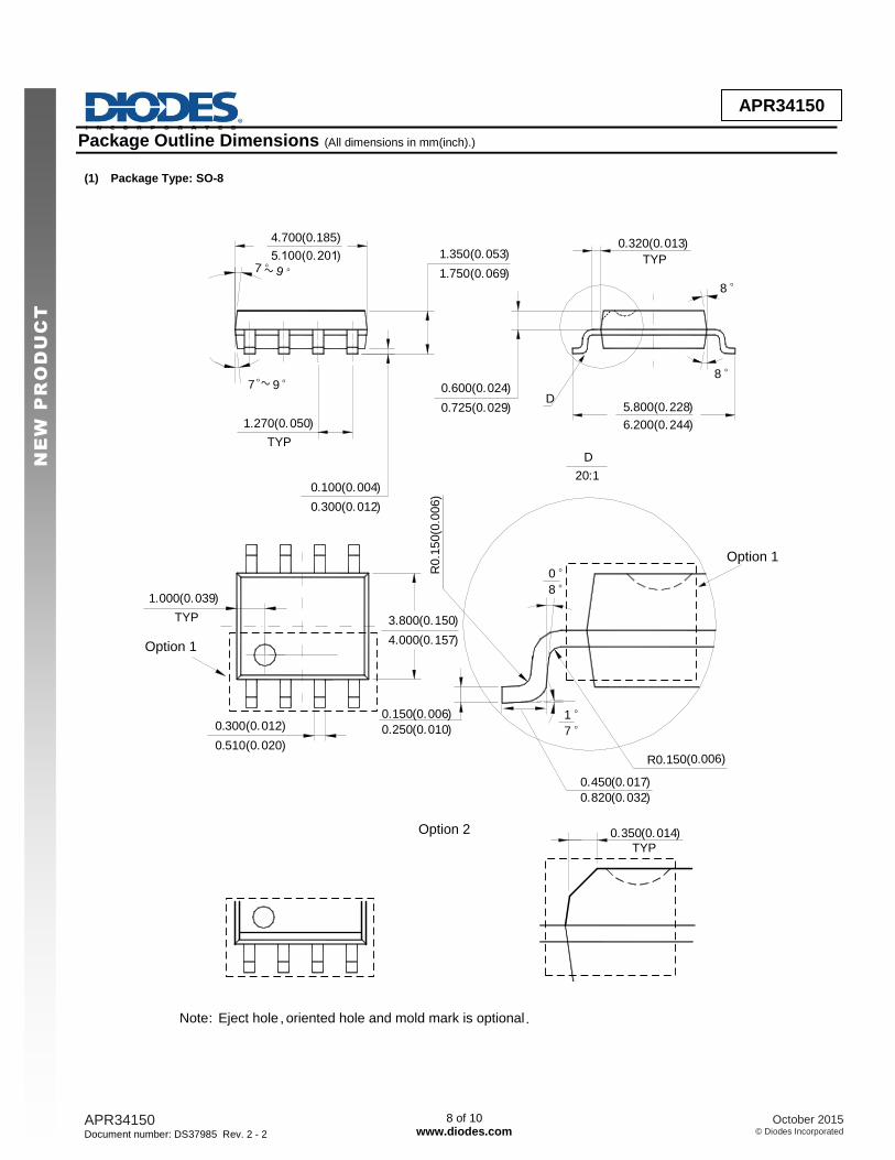
Package Outline Dimensions (All dimensions in mm(inch).)
(1) Package Type: SO-8
0°
8°
1°
7°
R0.150(0.006)
R0.1
50(0
.006)
1.000(0.039)
0.300(0.012)
0.510(0.020)
1.350(0.053)
1.750(0.069)
0.100(0.004)
0.300(0.012)
3.800(0.150)
4.000(0.157)
7°
7°
20:1
D
1.270(0.050)
TYP
0.150(0.006)
0.250(0.010)
8°
D5.800(0.228)
6.200(0.244)
0.600(0.024)
0.725(0.029)
0.320(0.013)
8°
0.450(0.017)
0.820(0.032)
4.700(0.185)
5.100(0.201)
Note: Eject hole , oriented hole and mold mark is optional.
Option 1
Option 1
Option 2 0.350(0.014)
TYP
TYP
TYP9°~
9°~
APR34150 Document number: DS37985 Rev. 2 - 2
9 of 10 www.diodes.com
October 2015 © Diodes Incorporated
APR34150
NE
W P
RO
DU
CT
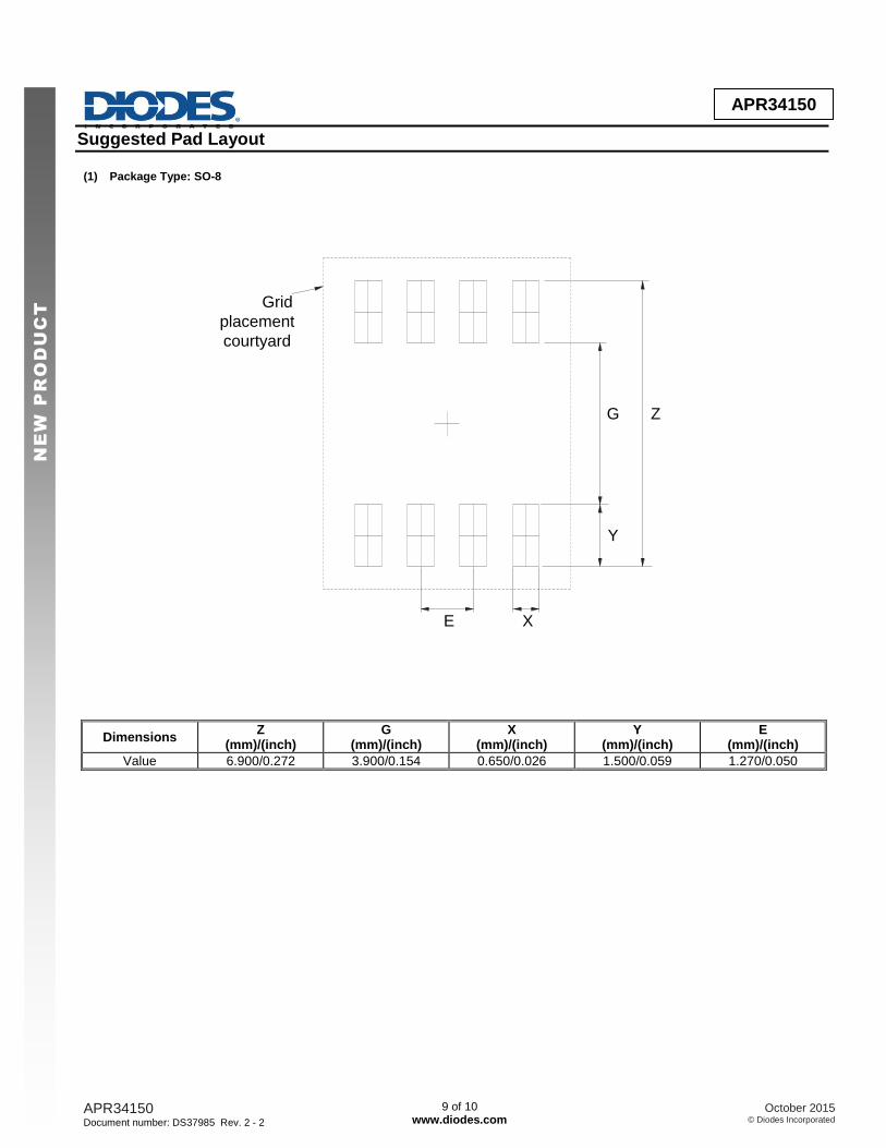
Suggested Pad Layout
(1) Package Type: SO-8
Grid
placement
courtyard
ZG
Y
E X
Dimensions Z
(mm)/(inch) G
(mm)/(inch) X
(mm)/(inch) Y
(mm)/(inch) E
(mm)/(inch)
Value 6.900/0.272 3.900/0.154 0.650/0.026 1.500/0.059 1.270/0.050
APR34150 Document number: DS37985 Rev. 2 - 2
10 of 10 www.diodes.com
October 2015 © Diodes Incorporated
APR34150
NE
W P
RO
DU
CT
IMPORTANT NOTICE DIODES INCORPORATED MAKES NO WARRANTY OF ANY KIND, EXPRESS OR IMPLIED, WITH REGARDS TO THIS DOCUMENT, INCLUDING, BUT NOT LIMITED TO, THE IMPLIED WARRANTIES OF MERCHANTABILITY AND FITNESS FOR A PARTICULAR PURPOSE (AND THEIR EQUIVALENTS UNDER THE LAWS OF ANY JURISDICTION). Diodes Incorporated and its subsidiaries reserve the right to make modifications, enhancements, improvements, corrections or other changes without further notice to this document and any product described herein. Diodes Incorporated does not assume any liability arising out of the application or use of this document or any product described herein; neither does Diodes Incorporated convey any license under its patent or trademark rights, nor the rights of others. Any Customer or user of this document or products described herein in such applications shall assume all risks of such use and will agree to hold Diodes Incorporated and all the companies whose products are represented on Diodes Incorporated website, harmless against all damages. Diodes Incorporated does not warrant or accept any liability whatsoever in respect of any products purchased through unauthorized sales channel. Should Customers purchase or use Diodes Incorporated products for any unintended or unauthorized application, Customers shall indemnify and hold Diodes Incorporated and its representatives harmless against all claims, damages, expenses, and attorney fees arising out of, directly or indirectly, any claim of personal injury or death associated with such unintended or unauthorized application. Products described herein may be covered by one or more United States, international or foreign patents pending. Product names and markings noted herein may also be covered by one or more United States, international or foreign trademarks. This document is written in English but may be translated into multiple languages for reference. Only the English version of this document is the final and determinative format released by Diodes Incorporated.
LIFE SUPPORT Diodes Incorporated products are specifically not authorized for use as critical components in life support devices or systems without the express written approval of the Chief Executive Officer of Diodes Incorporated. As used herein: A. Life support devices or systems are devices or systems which: 1. are intended to implant into the body, or
2. support or sustain life and whose failure to perform when properly used in accordance with instructions for use provided in the labeling can be reasonably expected to result in significant injury to the user.
B. A critical component is any component in a life support device or system whose failure to perform can be reasonably expected to cause the failure of the life support device or to affect its safety or effectiveness. Customers represent that they have all necessary expertise in the safety and regulatory ramifications of their life support devices or systems, and acknowledge and agree that they are solely responsible for all legal, regulatory and safety-related requirements concerning their products and any use of Diodes Incorporated products in such safety-critical, life support devices or systems, notwithstanding any devices- or systems-related information or support that may be provided by Diodes Incorporated. Further, Customers must fully indemnify Diodes Incorporated and its representatives against any damages arising out of the use of Diodes Incorporated products in such safety-critical, life support devices or systems. Copyright © 2015, Diodes Incorporated www.diodes.com
![arXiv:1605.09721v1 [stat.ML] 31 May 2016 · problems, as demonstrated by deep learning systems such as Google’s Downpour SGD [DCM+12] and Microsoft’s Project Adam [CSAK14]. While](https://static.fdocument.org/doc/165x107/5f0b45727e708231d42fb0f8/arxiv160509721v1-statml-31-may-2016-problems-as-demonstrated-by-deep-learning.jpg)