Device Noise Simulation of Delta-Sigma · PDF fileDevice Noise Simulation of ΔΣ...
23
The Designer’s Guide Community downloaded from www.designers-guide.org Copyright © 2006, Manolis Terrovitis and Kenneth S. Kundert – All Rights Reserved 1 of 23 Version 1, 24 August 1999 This report describes behavioral simulation of ΔΣ analog to digital converters including the effects of device noise. Simulation of the feedback loop filters with SpectreRF pro- vides the statistics of the device noise. A discrete time filter is used to generate noise with similar power spectral density (PSD) during the behavioral simulation. A second order converter is used to demonstrate the methodology and the simulation results are presented. Our approach does not make assumptions about the device and quantization noise adding linearly and takes into account their interaction. It is numerically efficient, as the behavioral simulation does not require significantly higher computational effort than in the case that device noise is not included. The same approach can be applied to continuous time converters. Originally written in August 1999, was first published in April 2003. Last updated on May 12, 2006. You can find the most recent version at www.designers-guide.org. Permission to make copies, either paper or electronic, of this work for personal or classroom use is granted without fee provided that the copies are not made or distributed for profit or commercial advantage and that the copies are complete and unmodified. To distribute other- wise, to publish, to post on servers, or to distribute to lists, requires prior written permission. Device Noise Simulation of ΔΣ Modulators Manolis Terrovitis and Ken Kundert
Transcript of Device Noise Simulation of Delta-Sigma · PDF fileDevice Noise Simulation of ΔΣ...
The Designer’s Guide Community downloaded from www.designers-guide.org
Device Noise Simulation of ΔΣ Modulators
Manolis Terrovitis and Ken Kundert
Version 1, 24 August 1999 This report describes behavioral simulation of ΔΣ analog to digital converters includingthe effects of device noise. Simulation of the feedback loop filters with SpectreRF pro-vides the statistics of the device noise. A discrete time filter is used to generate noisewith similar power spectral density (PSD) during the behavioral simulation. A secondorder converter is used to demonstrate the methodology and the simulation results arepresented. Our approach does not make assumptions about the device and quantizationnoise adding linearly and takes into account their interaction. It is numerically efficient,as the behavioral simulation does not require significantly higher computational effortthan in the case that device noise is not included. The same approach can be applied tocontinuous time converters.
Originally written in August 1999, was first published in April 2003. Last updated on May 12,2006. You can find the most recent version at www.designers-guide.org.
Permission to make copies, either paper or electronic, of this work for personal or classroomuse is granted without fee provided that the copies are not made or distributed for profit orcommercial advantage and that the copies are complete and unmodified. To distribute other-wise, to publish, to post on servers, or to distribute to lists, requires prior written permission.
Copyright © 2006, Manolis Terrovitis and Kenneth S. Kundert – All Rights Reserved 1 of 23
Device Noise Simulation of ΔΣ Modulators Introduction
1 Introduction
Delta-Sigma (ΔΣ) data converters are widely used, particularly in applications wherehigh precision is required and the signal band is relatively small, such as in the process-ing of audio and sensor signals. They are inherently insensitive to process imperfectionssuch as component mismatch and they can be easily integrated in inexpensive CMOStechnologies. Receiver architectures that employ band-pass ΔΣ A/D converters toreplace part of the analog RF part have been proposed [4, 5].
Because ΔΣ converters are large mixed-signal circuits and their performance character-ization requires extremely long transient simulations, transistor level simulation isimpractical because of time limitations. Behavioral simulation is used instead to test thefunctionality of a design. The behavioral models of the building blocks can include sec-ond-order effects such as finite opamp gain, finite opamp slew rate, component mis-match and nonlinearities [13]. It is the subject of this study to include device noise in thebehavioral models.
Although device noise is often a limiting factor in the performance of ΔΣ data convert-ers, it is not usually taken into account in simulations. Simulating noise with a circuitsimulator at the transistor level is impractical as explained above. In addition, circuitsimulators that are capable of providing the noise PSD at the output of circuits with atime-varying operating point, such as the Cadence analog simulator Spectre®RF†,require a periodically changing operating point. The operating point of ΔΣ converters ingeneral changes in a non-periodic fashion even for a DC input [1].
In this report we describe the device noise characterization of the building blocks of theconverter, and the subsequent behavioral simulation. To demonstrate the proposed meth-odology, we use a discrete time second-order ΔΣ converter as an example. The Spectr-eRF analog simulator is used for characterization of the building blocks. Whencompared with the usual behavioral simulation of ΔΣ converters, the proposed method-ology does not require more timesteps and does not significantly increase the computa-tional effort. This is a significant advantage compared to other suggested approaches[12]. Because of the multitude of architectures used in ΔΣ converters, the designer willprobably need to modify the presented methodology to fit its own needs.
2 ΔΣ AD Converter Background
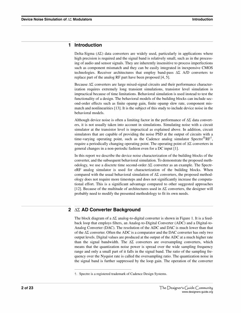
The block diagram of a ΔΣ analog-to-digital converter is shown in Figure 1. It is a feed-back loop that employs filters, an Analog-to-Digital Converter (ADC) and a Digital-to-Analog Converter (DAC). The resolution of the ADC and DAC is much lower than thatof the ΔΣ converter. Often the ADC is a comparator and the DAC converter has only twooutput levels. Digital values are produced at the output of the ADC at a much higher ratethan the signal bandwidth. The ΔΣ converters are oversampling converters, whichmeans that the quantization noise power is spread over the wide sampling frequencyrange and only a small part of it falls in the signal band. The ratio of the sampling fre-quency over the Nyquist rate is called the oversampling ratio. The quantization noise inthe signal band is further suppressed by the loop gain. The operation of the converter
†. Spectre is a registered trademark of Cadence Design Systems.
2 of 23 The Designer’s Guide Communitywww.designers-guide.org
ΔΣ AD Converter Background Device Noise Simulation of ΔΣ Modulators
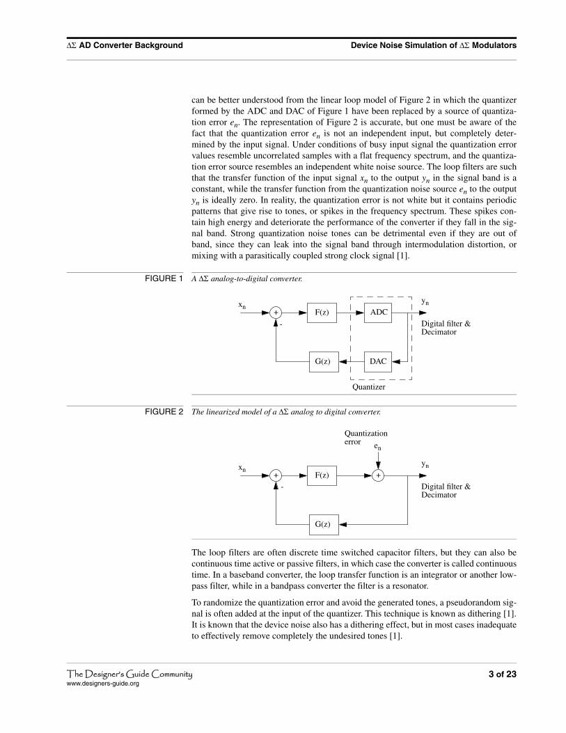
can be better understood from the linear loop model of Figure 2 in which the quantizerformed by the ADC and DAC of Figure 1 have been replaced by a source of quantiza-tion error en. The representation of Figure 2 is accurate, but one must be aware of thefact that the quantization error en is not an independent input, but completely deter-mined by the input signal. Under conditions of busy input signal the quantization errorvalues resemble uncorrelated samples with a flat frequency spectrum, and the quantiza-tion error source resembles an independent white noise source. The loop filters are suchthat the transfer function of the input signal xn to the output yn in the signal band is aconstant, while the transfer function from the quantization noise source en to the outputyn is ideally zero. In reality, the quantization error is not white but it contains periodicpatterns that give rise to tones, or spikes in the frequency spectrum. These spikes con-tain high energy and deteriorate the performance of the converter if they fall in the sig-nal band. Strong quantization noise tones can be detrimental even if they are out ofband, since they can leak into the signal band through intermodulation distortion, ormixing with a parasitically coupled strong clock signal [1].
The loop filters are often discrete time switched capacitor filters, but they can also becontinuous time active or passive filters, in which case the converter is called continuoustime. In a baseband converter, the loop transfer function is an integrator or another low-pass filter, while in a bandpass converter the filter is a resonator.
To randomize the quantization error and avoid the generated tones, a pseudorandom sig-nal is often added at the input of the quantizer. This technique is known as dithering [1].It is known that the device noise also has a dithering effect, but in most cases inadequateto effectively remove completely the undesired tones [1].
FIGURE 1 A ΔΣ analog-to-digital converter.
FIGURE 2 The linearized model of a ΔΣ analog to digital converter.
F(z) ADCDigital filter &Decimator
+
DACG(z)
xnyn
Quantizer
-
F(z)Digital filter &Decimator
+
G(z)
xnyn
-+
en
Quantizationerror
3 of 23The Designer’s Guide Communitywww.designers-guide.org
Device Noise Simulation of ΔΣ Modulators Methodology
The order of the delta-sigma converter is defined as the order of the loop transfer func-tion. The higher the order the better the noise suppression, but usually designs of orderhigher than two are prone to instability. An alternative that effectively implementshigher order noise suppression is the cascaded, or multistage, or MASH (MultistageNoise Shaping), converters. In these, the quantization error of a low order converter isprocessed as an input to another ΔΣ converter. Digital logic combines the outputs of allstages to one output, and ideally the resulting conversion is equivalent to that of a singlestage converter of order equal to the sum of the orders of all individual stages. The pro-posed methodology can be used for discrete or continuous time converters, and can beadapted for cascaded converters. If dithering is employed it can be simulated simulta-neously with the device noise.
3 Methodology
The analog circuitry of a ΔΣ converter contributes device noise, which together with thequantization noise, contaminates the output. In cases where in the signal band one of thetwo sources of noise is much lower than the other, the weak one can be neglected. If thequantization error is dominant, its effect can be simulated in the behavioral level as iscommonly done with Midas [14], Matlab, a programming language such as c, or Ver-ilog-A [7,15]. If the quantization noise is very low in the signal band as in cases wherethe oversampling ratio is very high and there are not tones of accumulated energy, itseffect can be neglected, and the in-band device noise alone suffices to be considered. Ifit is known that the quantization error truly resembles white noise and that the linearmodel of Figure 2 holds, the output device and quantization noise can be found sepa-rately as if the other source were not present, and then added to obtain the total outputnoise.
In the general case however both sources of error are present and the device noiseaffects the quantization noise. In particular, if one source of noise is negligible, designresources have probably been wasted. In wideband applications, the oversampling ratiocannot be very high and the quantization noise cannot be arbitrarily low. The out-of-band device noise indirectly has an effect on the performance because it affects the in-band quantization noise.
Since the digital filter reads periodically the ADC output and the signal fed backthrough the DAC must be exactly what the digital filter reads, the ADC must be clockedwith latched output, in both discrete and continuous time ΔΣ converters. Therefore, thedevice noise that the analog circuitry generates can be represented by a discrete timenoise process injected at the input of the ADC. With the proposed methodology thecombined effect of the device and quantization noise can be estimated. It can be summa-rized in the following steps
• The noise performance of the analog circuits involved in the loop is characterizedand the PSD of the equivalent discrete time noise process at the quantizer input isdetermined.
• A discrete time filter is found, which when fed with white noise, generates noisewith PSD similar to that of the equivalent noise.
• Time domain behavioral simulation with a representative input signal is run, simi-larly to how it is done for quantization noise effects in [13, 14]. In addition, noisegenerated by the discrete time filter is injected at the input of the ADC. The fre-
4 of 23 The Designer’s Guide Communitywww.designers-guide.org
Device Noise Estimation Device Noise Simulation of ΔΣ Modulators
quency spectrum of the time domain output reveals the quality of the data conver-sion. The behavioral models used for the building blocks can be otherwise ideal, orthey can include other nonidealities, as described in [13]. Dithering can also bepresent in the simulation.
4 Device Noise Estimation
A necessary assumption in the noise characterization of the analog part is that the gener-ated device noise is independent of the input signal and the ADC output, which is ingeneral a non-periodic signal. The assumption that the generated noise is independent ofthe input signal is usually made in the characterization of switched capacitor and contin-uous time active filters, similar to those used in discrete and continuous time ΔΣ con-verters respectively. It is usually accurate and it will be discussed in detail for theexample circuit of Section 5 on page 8.
Let us consider first discrete time ΔΣ converters. The operating point of the devices inthe switched capacitor filter changes wildly during the clock period. Assuming as wementioned above that the generated device noise is independent of the processed signal,noise at the input of the ADC is a continuous time cyclostationary process u(t) with PSDSu(f, t). Let t0 denote the time instant within the clock period at which this process issampled by the ADC, and ud(nTs) denote the resulting discrete-time noise process. It isintuitive and also easy to show that sampling a cyclostationary process once in a periodresults in a stationary discrete time process. The PSD of ud(nTs) is†
(1)
The Cadence analog simulator SpectreRF is capable of accurately predicting the noiseperformance of switched capacitor circuits [8, 9]. It is a continuous time simulator andprovides the time average noise PSD. To extract , an ideal sample and hold cir-cuit (S/H) can be employed, which samples the noise process u(t) at time t0 and holdsthis value for a whole period.‡ Let us denote the piecewise constant output of the S/Hcircuit with ush(t). It can be easily shown that this is a cyclostationary process and thetime average of its PSD is related with the PSD of ud(n) by
†. We are using here the following definition for
where is the autocorrelation function of ud(nTs). If it is desirable to find the power of
ud(nTs) one should integrate as given by the following equations from 0 to fs/2, if the
PSD Su( f, t) of the continuous time processes on the other side of the equation is single sided,or from 0 to fs if it is double sided. SpectreRF provides single-sided PSDs.
Sudf( )
Sudf( ) Ts Rud
kTs( )ej– k2πTs f
k ∞–=
∞
∑=
RudkTs( )
Sudf( )
Sudf( ) Su f kfs– t0,( )
k ∞–=
∞
∑=
Sudf( )
Sushf( )
5 of 23The Designer’s Guide Communitywww.designers-guide.org
Device Noise Simulation of ΔΣ Modulators Device Noise Estimation
(2)
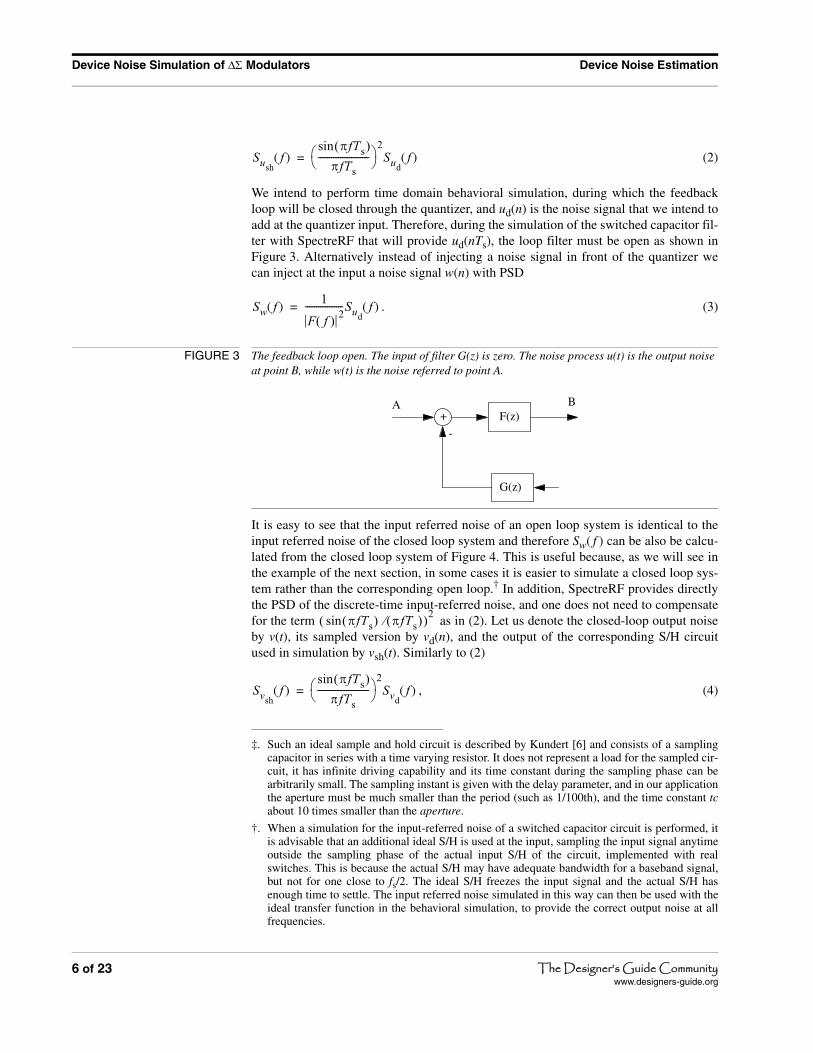
We intend to perform time domain behavioral simulation, during which the feedbackloop will be closed through the quantizer, and ud(n) is the noise signal that we intend toadd at the quantizer input. Therefore, during the simulation of the switched capacitor fil-ter with SpectreRF that will provide ud(nTs), the loop filter must be open as shown inFigure 3. Alternatively instead of injecting a noise signal in front of the quantizer wecan inject at the input a noise signal w(n) with PSD
. (3)
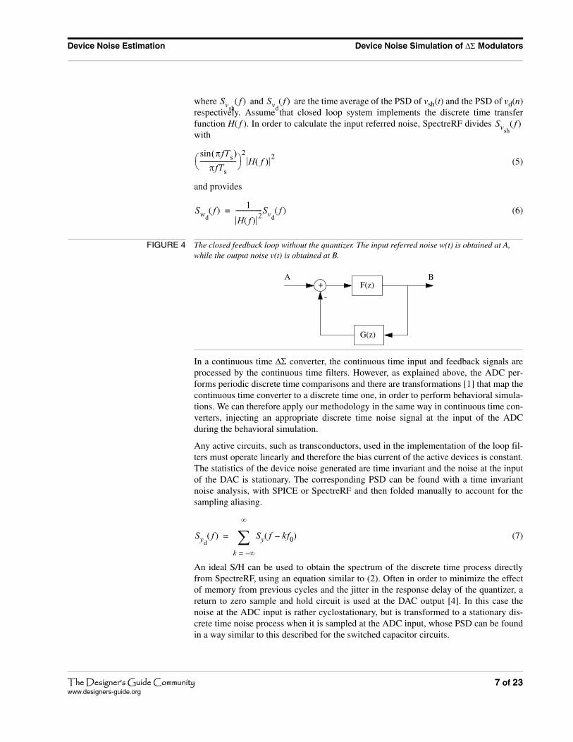
It is easy to see that the input referred noise of an open loop system is identical to theinput referred noise of the closed loop system and therefore Sw( f ) can be also be calcu-lated from the closed loop system of Figure 4. This is useful because, as we will see inthe example of the next section, in some cases it is easier to simulate a closed loop sys-tem rather than the corresponding open loop.† In addition, SpectreRF provides directlythe PSD of the discrete-time input-referred noise, and one does not need to compensatefor the term as in (2). Let us denote the closed-loop output noiseby v(t), its sampled version by vd(n), and the output of the corresponding S/H circuitused in simulation by vsh(t). Similarly to (2)
, (4)
‡. Such an ideal sample and hold circuit is described by Kundert [6] and consists of a samplingcapacitor in series with a time varying resistor. It does not represent a load for the sampled cir-cuit, it has infinite driving capability and its time constant during the sampling phase can bearbitrarily small. The sampling instant is given with the delay parameter, and in our applicationthe aperture must be much smaller than the period (such as 1/100th), and the time constant tcabout 10 times smaller than the aperture.
FIGURE 3 The feedback loop open. The input of filter G(z) is zero. The noise process u(t) is the output noise at point B, while w(t) is the noise referred to point A.
†. When a simulation for the input-referred noise of a switched capacitor circuit is performed, itis advisable that an additional ideal S/H is used at the input, sampling the input signal anytimeoutside the sampling phase of the actual input S/H of the circuit, implemented with realswitches. This is because the actual S/H may have adequate bandwidth for a baseband signal,but not for one close to fs/2. The ideal S/H freezes the input signal and the actual S/H hasenough time to settle. The input referred noise simulated in this way can then be used with theideal transfer function in the behavioral simulation, to provide the correct output noise at allfrequencies.
Sushf( )
πfTs( )sinπfTs
-----------------------⎝ ⎠⎛ ⎞
2Sud
f( )=
Sw f( )1
F f( ) 2-----------------Sud
f( )=
F(z)+
G(z)
-
BA
πfTs( )sin πfTs( )⁄( )2
Svshf( )
πfTs( )sinπfTs
-----------------------⎝ ⎠⎛ ⎞
2Svd
f( )=
6 of 23 The Designer’s Guide Communitywww.designers-guide.org
Device Noise Estimation Device Noise Simulation of ΔΣ Modulators
where and are the time average of the PSD of vsh(t) and the PSD of vd(n)respectively. Assume that closed loop system implements the discrete time transferfunction H( f ). In order to calculate the input referred noise, SpectreRF divides with
(5)
and provides
(6)
In a continuous time ΔΣ converter, the continuous time input and feedback signals areprocessed by the continuous time filters. However, as explained above, the ADC per-forms periodic discrete time comparisons and there are transformations [1] that map thecontinuous time converter to a discrete time one, in order to perform behavioral simula-tions. We can therefore apply our methodology in the same way in continuous time con-verters, injecting an appropriate discrete time noise signal at the input of the ADCduring the behavioral simulation.
Any active circuits, such as transconductors, used in the implementation of the loop fil-ters must operate linearly and therefore the bias current of the active devices is constant.The statistics of the device noise generated are time invariant and the noise at the inputof the DAC is stationary. The corresponding PSD can be found with a time invariantnoise analysis, with SPICE or SpectreRF and then folded manually to account for thesampling aliasing.
(7)
An ideal S/H can be used to obtain the spectrum of the discrete time process directlyfrom SpectreRF, using an equation similar to (2). Often in order to minimize the effectof memory from previous cycles and the jitter in the response delay of the quantizer, areturn to zero sample and hold circuit is used at the DAC output [4]. In this case thenoise at the ADC input is rather cyclostationary, but is transformed to a stationary dis-crete time noise process when it is sampled at the ADC input, whose PSD can be foundin a way similar to this described for the switched capacitor circuits.
FIGURE 4 The closed feedback loop without the quantizer. The input referred noise w(t) is obtained at A, while the output noise v(t) is obtained at B.
Svshf( ) Svd
f( )
Svshf( )
πfTs( )sinπfTs
-----------------------⎝ ⎠⎛ ⎞
2H f( ) 2
Swdf( )
1
H f( )2
-----------------Svdf( )=
F(z)+
G(z)
-
BA
Sydf( ) Sy f kf0–( )
k ∞–=
∞
∑=
7 of 23The Designer’s Guide Communitywww.designers-guide.org
Device Noise Simulation of ΔΣ Modulators Example: A 2nd Order ΔΣ Converter
Noise and any nonideality of the ADC are rather insignificant. It is important to noticethat when a wrong decision taken by the ADC and read by the digital filter, the samewrong decision is fed back to the input, and will be corrected for in the future cycles.The in-band input referred noise of the ADC gets suppressed by the feedback loop in away similar to the quantization noise. The out-of-band noise however could have aneffect on the quantization noise, but this effect is unlikely very significant.
The device noise of the DAC does not get suppressed by any mechanism has a directeffect on the in band noise and it also affects the quantization noise.
5 Example: A 2nd Order ΔΣ Converter
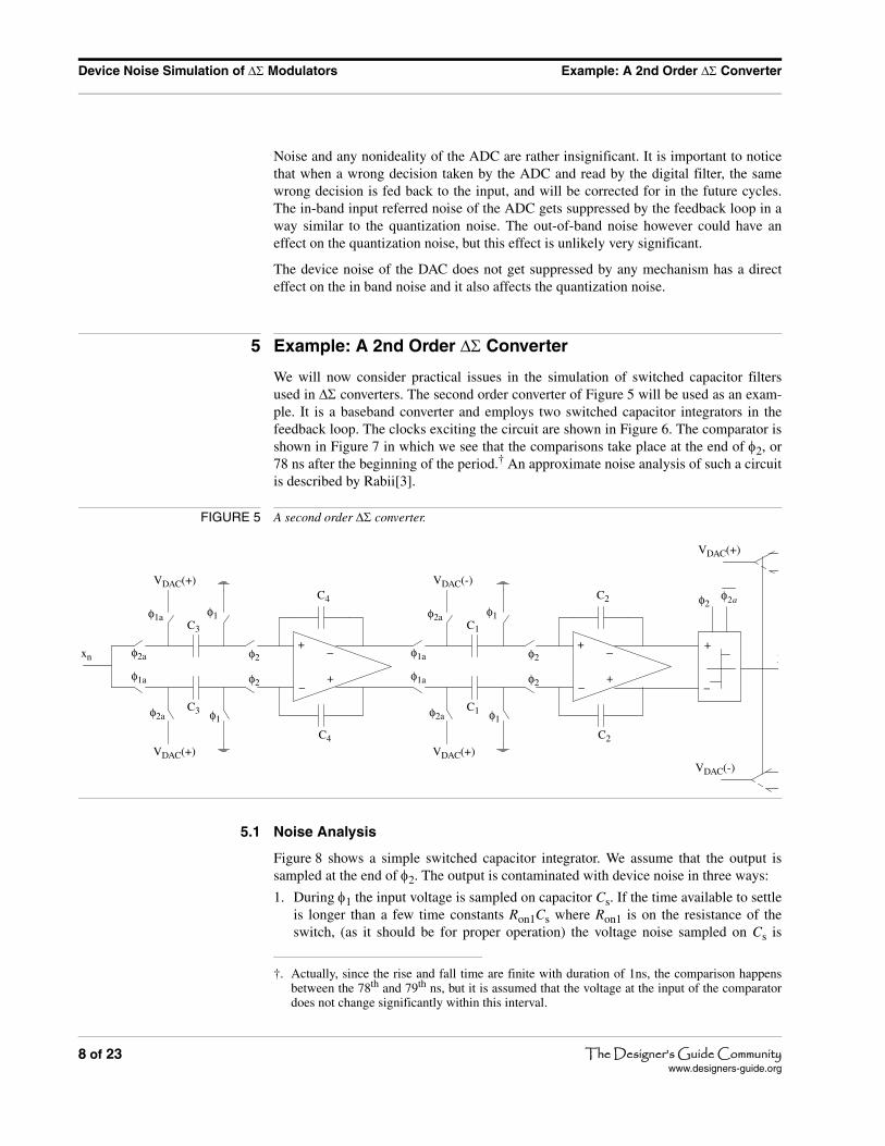
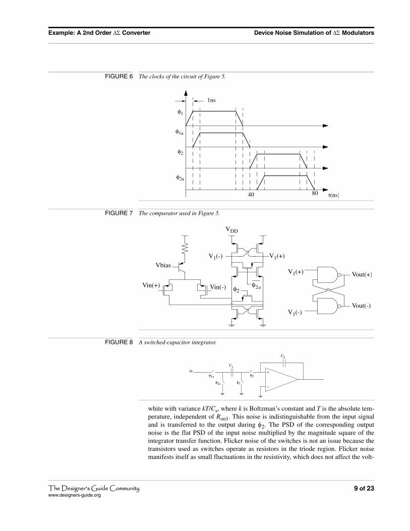
We will now consider practical issues in the simulation of switched capacitor filtersused in ΔΣ converters. The second order converter of Figure 5 will be used as an exam-ple. It is a baseband converter and employs two switched capacitor integrators in thefeedback loop. The clocks exciting the circuit are shown in Figure 6. The comparator isshown in Figure 7 in which we see that the comparisons take place at the end of φ2, or78 ns after the beginning of the period.† An approximate noise analysis of such a circuitis described by Rabii[3].
5.1 Noise Analysis
Figure 8 shows a simple switched capacitor integrator. We assume that the output issampled at the end of φ2. The output is contaminated with device noise in three ways:
1. During φ1 the input voltage is sampled on capacitor Cs. If the time available to settleis longer than a few time constants Ron1Cs where Ron1 is on the resistance of theswitch, (as it should be for proper operation) the voltage noise sampled on Cs is
†. Actually, since the rise and fall time are finite with duration of 1ns, the comparison happensbetween the 78th and 79th ns, but it is assumed that the voltage at the input of the comparatordoes not change significantly within this interval.
FIGURE 5 A second order ΔΣ converter.
+
_ +
C4
C4
φ1
−
φ1
φ2
φ2
φ1a
φ1a
φ2a
φ2a
xn
C3
C3
VDAC(+)
VDAC(+)
+
_ +
C2
C2
φ1
−
φ1
φ2
φ2
φ2a
φ1a
φ1a
φ2a
C1
C1
VDAC(-)
VDAC(+)
+
_
φ2φ2a
y
VDAC(+)
VDAC(-)
8 of 23 The Designer’s Guide Communitywww.designers-guide.org
Example: A 2nd Order ΔΣ Converter Device Noise Simulation of ΔΣ Modulators
white with variance kT/Cs, where k is Boltzman’s constant and T is the absolute tem-perature, independent of Ron1. This noise is indistinguishable from the input signaland is transferred to the output during φ2. The PSD of the corresponding outputnoise is the flat PSD of the input noise multiplied by the magnitude square of theintegrator transfer function. Flicker noise of the switches is not an issue because thetransistors used as switches operate as resistors in the triode region. Flicker noisemanifests itself as small fluctuations in the resistivity, which does not affect the volt-
FIGURE 6 The clocks of the circuit of Figure 5.
FIGURE 7 The comparator used in Figure 5.
FIGURE 8 A switched-capacitor integrator.
φ1
φ1a
φ2
φ2a
t(ns)80
1ns
40
φ2φ2a
V1(+)V1(-)
VDD
Vin(-)Vin(+)
Vbias
Vout(+)
Vout(-)
V1(+)
V1(-)
+
_
CI
φ1
φ2φ1a
φ2a
Csin
9 of 23The Designer’s Guide Communitywww.designers-guide.org
Device Noise Simulation of ΔΣ Modulators Example: A 2nd Order ΔΣ Converter
ages sampled on the capacitors since at the end of every phase there is no currentpassing through them.
2. During φ2 the circuit generates broadband noise, which when sampled at the outputat the end of φ2 is converted to discrete time noise process and its spectrum is folded.The transistors of the opamp as well as the on switches contribute to this noise. If theopamp were ideal with infinite gain at all frequencies the switches would contributeagain noise with power kT/Cs on Cs, or (kT/Cs)(Cs/CI)
2 to the output, but in practicethis noise contribution is a function of the bandwidth of the opamp and generallydepends on the on resistance of the switches Ron2. The contribution of the opampalso depends on Ron2. In most practical cases however the broadband noise is practi-cally independent of Ron2 [2].
3. At the end of φ2 some of the broadband noise is stored on CI, which affects the out-put in future cycles since this capacitor is never reset. It is equivalent to consider thatthe charge that corresponds to this noise is stored on Cs during the next φ1 (this hap-pens to be equal to the noise sampled on Cs at the end of φ2). As in Item 1, noisestored on Cs is indistinguishable from the input signal and its PSD is transferred tothe output by multiplication with the magnitude square of the integrator transferfunction. This noise contribution however is correlated with that of Item 2.
5.2 Cyclostationarity
Here we justify the assumption that the noise generated in every cycle in independent ofthe processed signal.
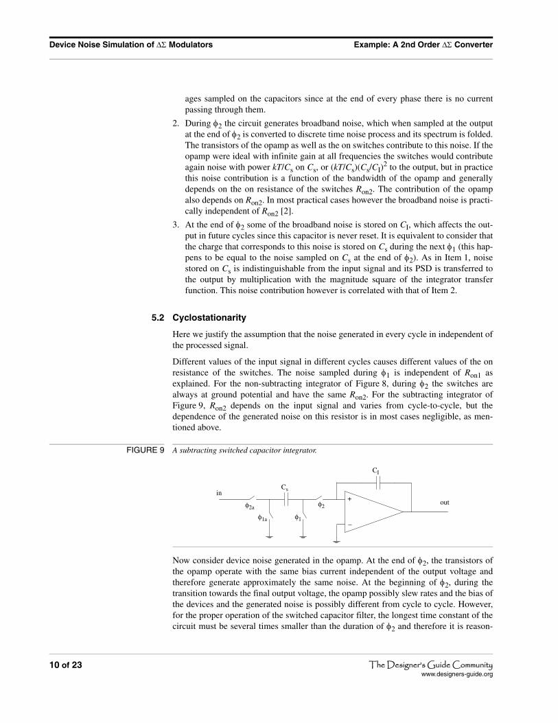
Different values of the input signal in different cycles causes different values of the onresistance of the switches. The noise sampled during φ1 is independent of Ron1 asexplained. For the non-subtracting integrator of Figure 8, during φ2 the switches arealways at ground potential and have the same Ron2. For the subtracting integrator ofFigure 9, Ron2 depends on the input signal and varies from cycle-to-cycle, but thedependence of the generated noise on this resistor is in most cases negligible, as men-tioned above.
Now consider device noise generated in the opamp. At the end of φ2, the transistors ofthe opamp operate with the same bias current independent of the output voltage andtherefore generate approximately the same noise. At the beginning of φ2, during thetransition towards the final output voltage, the opamp possibly slew rates and the bias ofthe devices and the generated noise is possibly different from cycle to cycle. However,for the proper operation of the switched capacitor filter, the longest time constant of thecircuit must be several times smaller than the duration of φ2 and therefore it is reason-
FIGURE 9 A subtracting switched capacitor integrator.
+
_
CI
φ1
φ2
φ1a
φ2a
Csin
out
10 of 23 The Designer’s Guide Communitywww.designers-guide.org
Example: A 2nd Order ΔΣ Converter Device Noise Simulation of ΔΣ Modulators
able to consider that the differences in the generated noise in the beginning of the phasehave faded at the end when the voltage sampling takes place. Considering flicker noise,the values of the flicker noise sources in the opamp are determined by the long termtime average bias and cannot be significantly different form cycle to cycle nor can theybe significantly affected by the slew rate time interval.
We justified that the statistics of the generated noise do not significantly vary from cycleto cycle and therefore is cyclostationary. The noise simulations intended to characterizethe noise performance of the switched capacitor filter can be performed without inputsignal.
5.3 Simulation
The reference by Kundert [8] gives some guidelines for the simulation of SC filters andshould be read carefully before one attempts to use SpectreRF for this purpose.Switched capacitor circuits are excited by the strong clock waveforms whose rise andfall time are much smaller than the period. SpectreRF is primarily configured for RF cir-cuits in which the strong periodic excitation is usually a smooth function. For this rea-son, the accuracy parameters of the simulator must usually be tightened in order toobtain a reliable result. It is recommended that in the PNoise analysis a large number ofsidebands should be requested to adequately account for noise folding, for examplemaxsideband=20. If there are very small time constants in the circuit compared to theperiod (e.g. fast sampling circuits), which give rise to wideband noise spectra, the max-sideband parameter should be higher so as to include more noise folding.
Simulating an open loop integrator, and even worse a cascade of integrators is vulnera-ble to convergence problems during the PSS analysis. A slight error in the initial inputvoltage gets integrated and results in a large difference at the output between the begin-ning and the end of the period. A small amount of feedback, such as an RC divider witha pole at very low frequencies is often necessary to make convergence possible. In somecases, in order to achieve convergence the introduced pole needs to be at frequencieshigh enough to affect the transfer function of the system and the output noise spectrumin the band of interest.†
A great improvement in the convergence problems and simulation time can be achieved,if instead of the output noise we seek the input referred noise of the cascade of the twointegrators. During the behavioral simulation we can add the corresponding noise signalat the input of the cascade, instead of the output. The input referred noise of the openloop system is equal to that of the close loop system with feedback gain equal to one (orany other noiseless feedback). This is equivalent to just simulating the loop of Figure 1without the quantizer. The close loop systems have better convergence properties duringthe PSS analysis and the simulation is generally faster.
†. It was found that PSS convergence is facilitated by performing a PSS analysis with a signifi-cant feedback (e.g. small resistor) in the beginning and saving the initial conditions in a file.The PSS analysis is then repeated several times by reducing the feedback and using the initialconditions generated in the previous simulation.
11 of 23The Designer’s Guide Communitywww.designers-guide.org
Device Noise Simulation of ΔΣ Modulators Example: A 2nd Order ΔΣ Converter
5.4 Closing the Loop
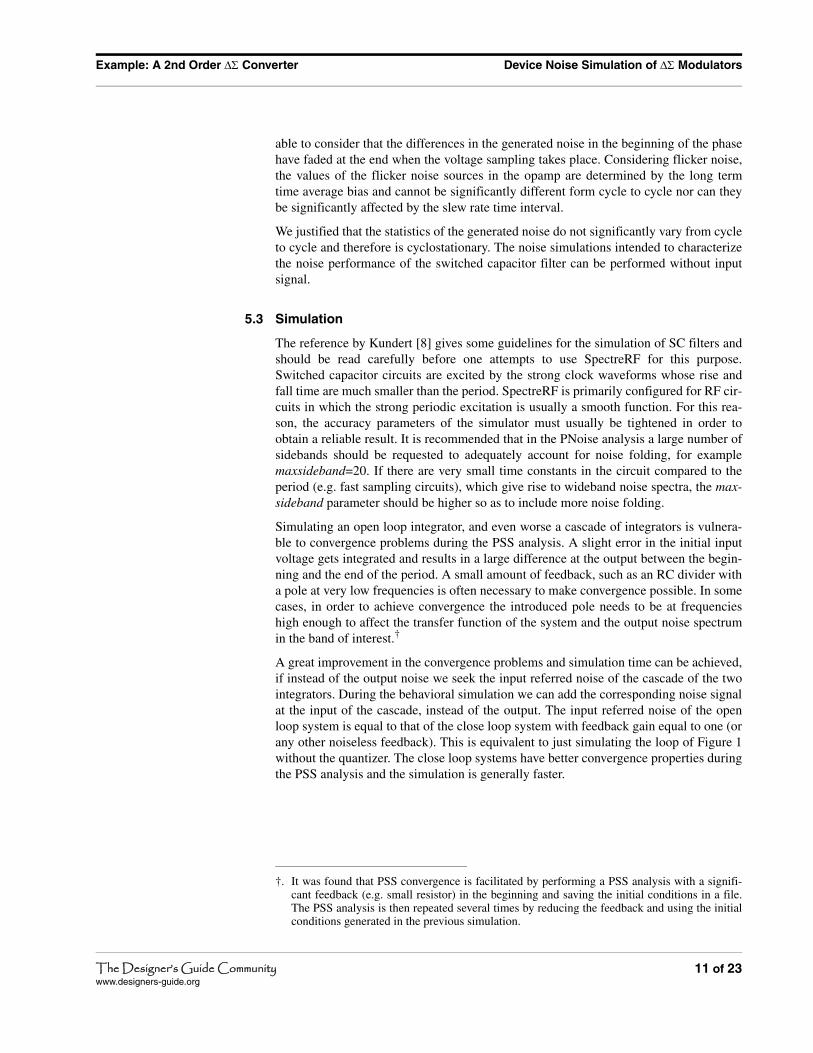
We will now discuss how to close the loop. Directly connecting the output to the input isincorrect, and in fact the input referred noise that simulation provides in this case is dif-ferent than that of the open loop system. A switched capacitor circuit is a discrete timesystem, and when closing the loop, during the output evaluation one must feed at theinput the output the previous cycle. Some kind of memory is needed to store the outputfor one cycle, and an ideal S/H can be used for this purpose. Consider the integrator ofFigure 8. It is important that to notice that although ignoring the noise, the output volt-age stays the same after the end of φ2, until the beginning of φ2 of the next cycle, theoutput noise must be sampled at the end of φ2 since after that the topology of the circuitchanges and the output noise is different. As shown in Figure 10, an ideal S/H can storethe output at the end of φ2 and provide it at the input during the next φ1 when it must beread. In a subtracting integrator where the input must be read during φ2, the output of theprevious cycle is not available during the whole φ2, because the S/H must obtain the newoutput at the same time. This problem can be easily solved with a second S/H, samplingthe output of the first anytime outside φ2, as shown in Figure 11.
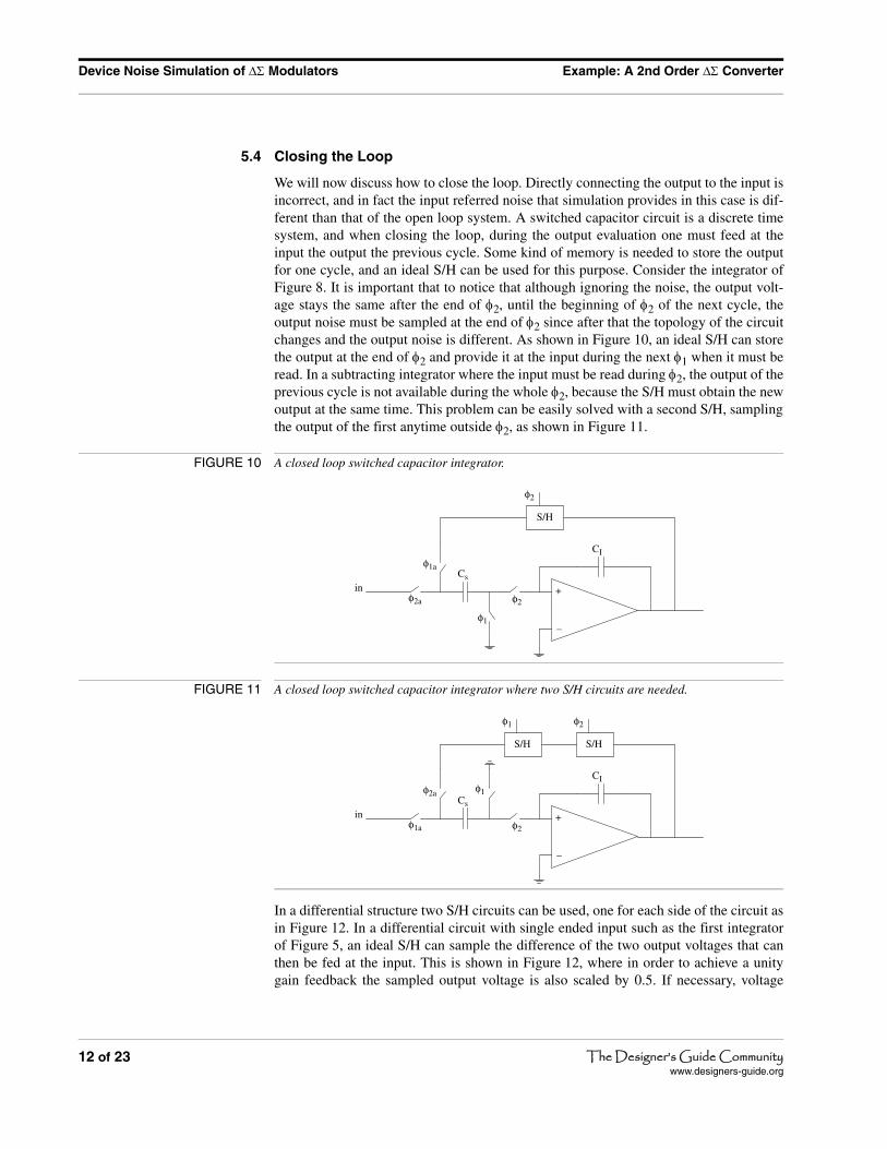
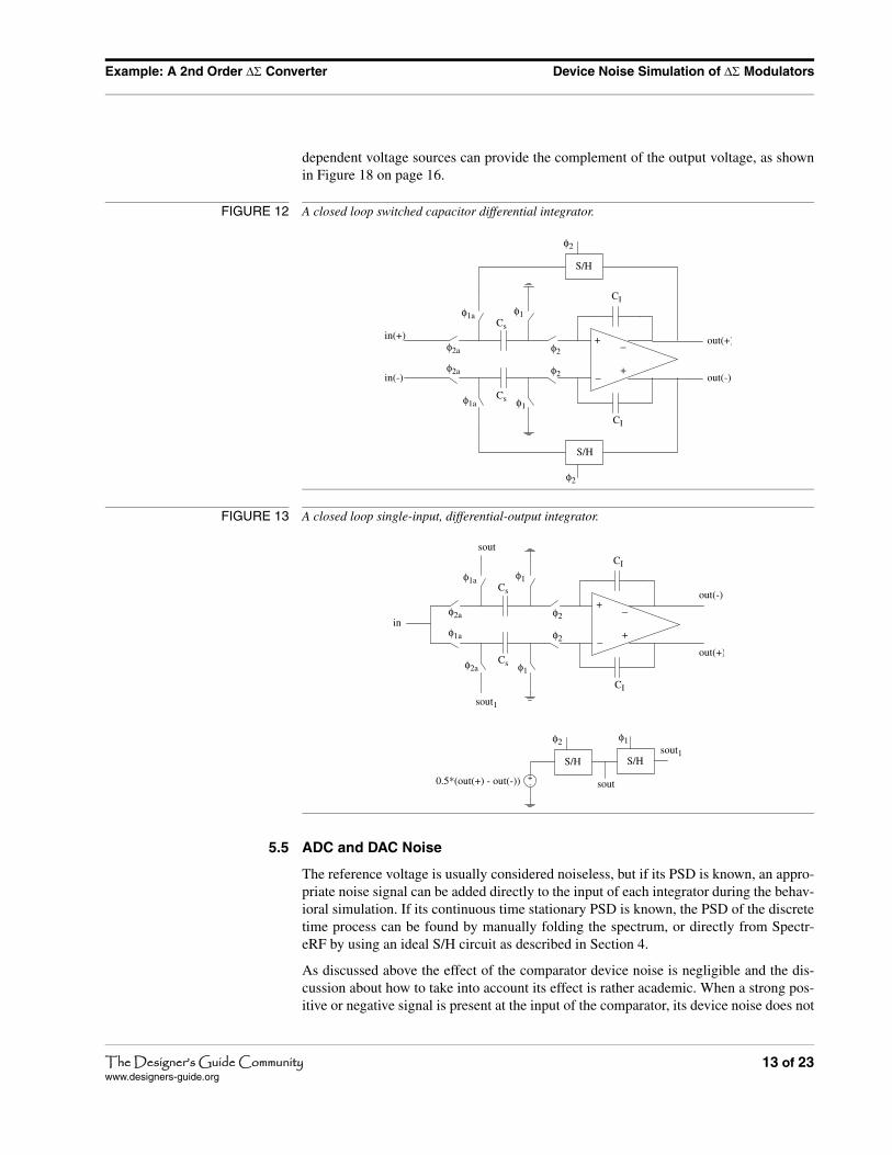
In a differential structure two S/H circuits can be used, one for each side of the circuit asin Figure 12. In a differential circuit with single ended input such as the first integratorof Figure 5, an ideal S/H can sample the difference of the two output voltages that canthen be fed at the input. This is shown in Figure 12, where in order to achieve a unitygain feedback the sampled output voltage is also scaled by 0.5. If necessary, voltage
FIGURE 10 A closed loop switched capacitor integrator.
FIGURE 11 A closed loop switched capacitor integrator where two S/H circuits are needed.
+
_
CI
φ1
φ2
φ1a
φ2a
Cs
S/H
φ2
in
+
_
CIφ1
φ2
φ2a
φ1a
Cs
S/H
φ1
in
S/H
φ2
12 of 23 The Designer’s Guide Communitywww.designers-guide.org
Example: A 2nd Order ΔΣ Converter Device Noise Simulation of ΔΣ Modulators
dependent voltage sources can provide the complement of the output voltage, as shownin Figure 18 on page 16.
5.5 ADC and DAC Noise
The reference voltage is usually considered noiseless, but if its PSD is known, an appro-priate noise signal can be added directly to the input of each integrator during the behav-ioral simulation. If its continuous time stationary PSD is known, the PSD of the discretetime process can be found by manually folding the spectrum, or directly from Spectr-eRF by using an ideal S/H circuit as described in Section 4.
As discussed above the effect of the comparator device noise is negligible and the dis-cussion about how to take into account its effect is rather academic. When a strong pos-itive or negative signal is present at the input of the comparator, its device noise does not
FIGURE 12 A closed loop switched capacitor differential integrator.
FIGURE 13 A closed loop single-input, differential-output integrator.
+
_ +
CI
CI
φ1
−
φ1
φ2
φ2
φ1a
φ2a
φ2a
φ1a
Cs
Cs
S/H
S/H
φ2
φ2
in(+)
in(-)
out(+)
out(-)
+
_ +
CI
CI
φ1
−
φ1
φ2
φ2
φ1a
φ1a
φ2a
φ2a
Cs
Cs
in
out(-)
out(+)
+-0.5*(out(+) - out(-))
S/H
φ2
sout
sout
sout1
S/H
φ1sout1
13 of 23The Designer’s Guide Communitywww.designers-guide.org
Device Noise Simulation of ΔΣ Modulators Example: A 2nd Order ΔΣ Converter
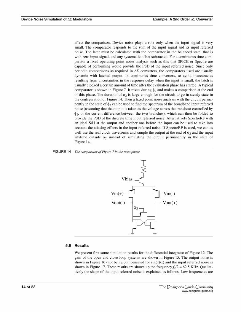
affect the comparison. Device noise plays a role only when the input signal is verysmall. The comparator responds to the sum of the input signal and its input referrednoise. The later must be calculated with the comparator in the balanced state, that iswith zero input signal, and any systematic offset subtracted. For a continuous time com-parator a fixed operating point noise analysis such as this that SPICE or Spectre arecapable of performing would provide the PSD of the input referred noise. Since onlyperiodic comparisons as required in ΔΣ converters, the comparators used are usuallydynamic with latched output. In continuous time converters, to avoid inaccuraciesresulting from uncertainties in the response delay when the input is small, the latch isusually clocked a certain amount of time after the evaluation phase has started. A typicalcomparator is shown in Figure 7. It resets during φ2 and makes a comparison at the endof this phase. The duration of φ2 is large enough for the circuit to go in steady state inthe configuration of Figure 14. Then a fixed point noise analysis with the circuit perma-nently in the state of φ2 can be used to find the spectrum of the broadband input referrednoise (assuming that the output is taken as the voltage across the transistor controlled byφ2, or the current difference between the two branches), which can then be folded toprovide the PSD of the discrete time input referred noise. Alternatively SpectreRF withan ideal S/H at the output and another one before the input can be used to take intoaccount the aliasing effects in the input referred noise. If SpectreRF is used, we can aswell use the real clock waveforms and sample the output at the end of φ2 and the inputanytime outside φ2 instead of simulating the circuit permanently in the state ofFigure 14.
5.6 Results
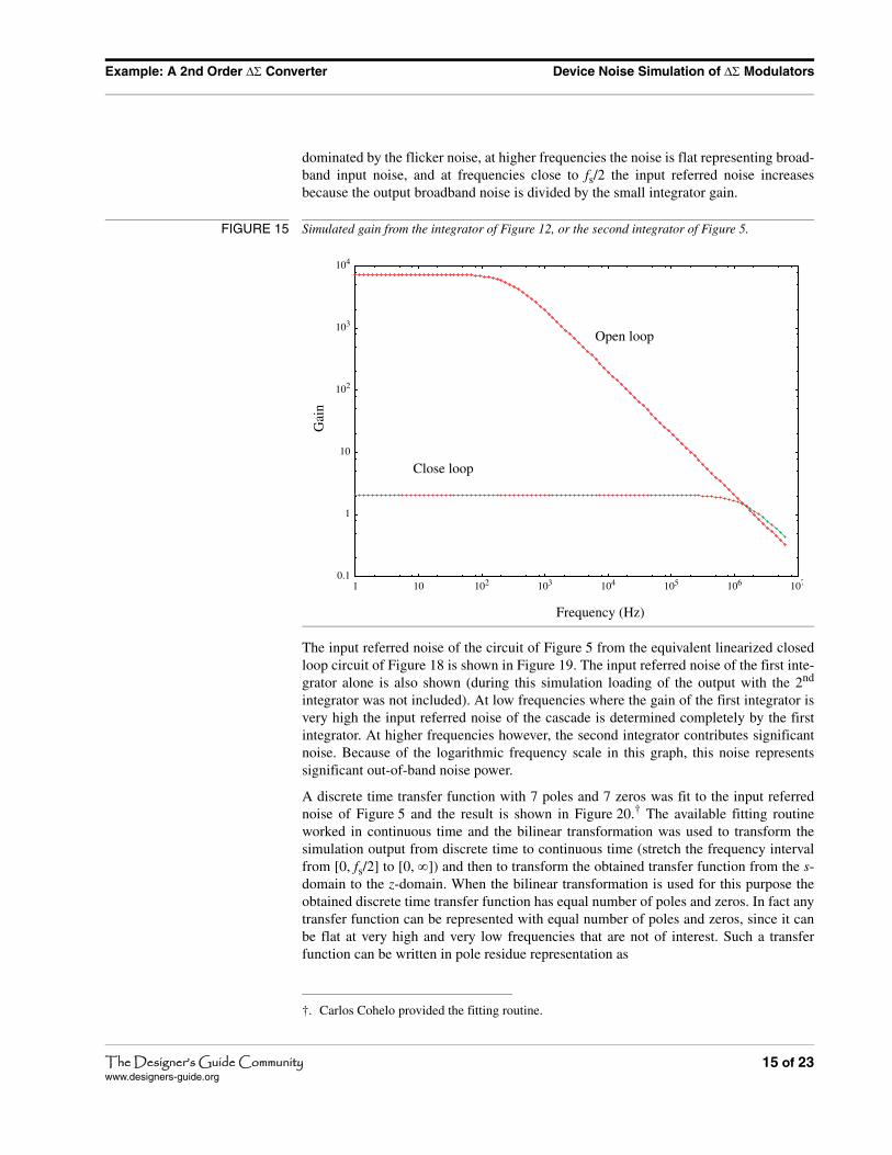
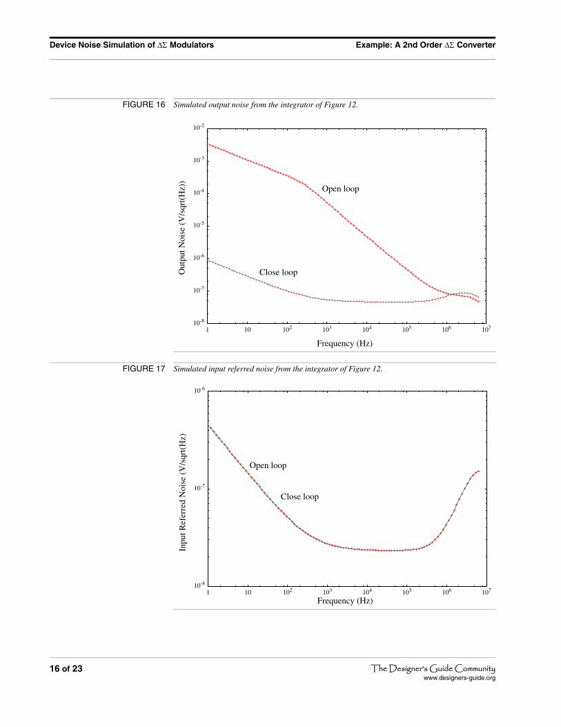
We present first some simulation results for the differential integrator of Figure 12. Thegain of the open and close loop systems are shown in Figure 15. The output noise isshown in Figure 16 (not being compensated for sin(x)/x) and the input referred noise isshown in Figure 17. These results are shown up the frequency fs/2 = 62.5 KHz. Qualita-tively the shape of the input referred noise is explained as follows. Low frequencies are
FIGURE 14 The comparator of Figure 7 in the reset phase.
φ2
Vin(-)Vin(+)
Vbias
Vout(-) Vout(+)
14 of 23 The Designer’s Guide Communitywww.designers-guide.org
Example: A 2nd Order ΔΣ Converter Device Noise Simulation of ΔΣ Modulators
dominated by the flicker noise, at higher frequencies the noise is flat representing broad-band input noise, and at frequencies close to fs/2 the input referred noise increasesbecause the output broadband noise is divided by the small integrator gain.
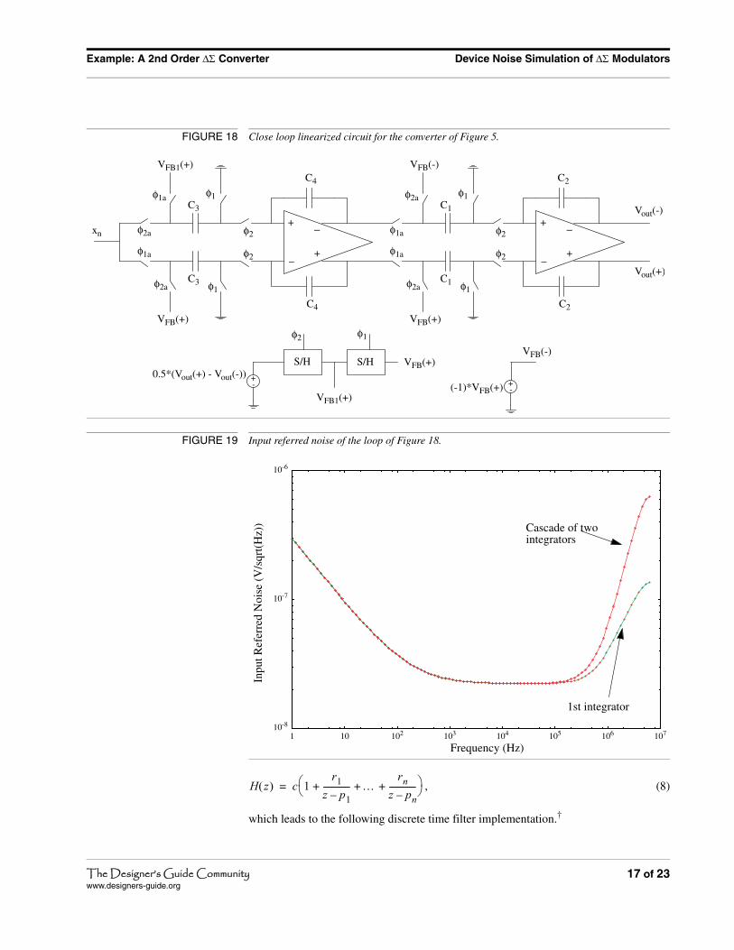
The input referred noise of the circuit of Figure 5 from the equivalent linearized closedloop circuit of Figure 18 is shown in Figure 19. The input referred noise of the first inte-grator alone is also shown (during this simulation loading of the output with the 2nd
integrator was not included). At low frequencies where the gain of the first integrator isvery high the input referred noise of the cascade is determined completely by the firstintegrator. At higher frequencies however, the second integrator contributes significantnoise. Because of the logarithmic frequency scale in this graph, this noise representssignificant out-of-band noise power.
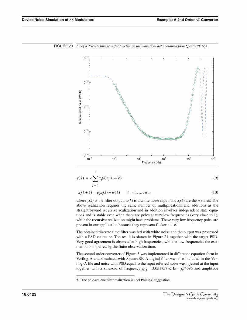
A discrete time transfer function with 7 poles and 7 zeros was fit to the input referrednoise of Figure 5 and the result is shown in Figure 20.† The available fitting routineworked in continuous time and the bilinear transformation was used to transform thesimulation output from discrete time to continuous time (stretch the frequency intervalfrom [0, fs/2] to [0, ∞]) and then to transform the obtained transfer function from the s-domain to the z-domain. When the bilinear transformation is used for this purpose theobtained discrete time transfer function has equal number of poles and zeros. In fact anytransfer function can be represented with equal number of poles and zeros, since it canbe flat at very high and very low frequencies that are not of interest. Such a transferfunction can be written in pole residue representation as
FIGURE 15 Simulated gain from the integrator of Figure 12, or the second integrator of Figure 5.
†. Carlos Cohelo provided the fitting routine.
0.1
1
10
102
103
104
1 10 102 103 104 105 106 107
Open loop
Close loop
Gai
n
Frequency (Hz)
15 of 23The Designer’s Guide Communitywww.designers-guide.org
Device Noise Simulation of ΔΣ Modulators Example: A 2nd Order ΔΣ Converter
FIGURE 16 Simulated output noise from the integrator of Figure 12.
FIGURE 17 Simulated input referred noise from the integrator of Figure 12.
10-8
10-7
10-6
10-5
10-4
10-3
10-2
1 10 102 103 104 105 106 107
Frequency (Hz)
Out
put N
oise
(V
/sqr
t(H
z))
Open loop
Close loop
10-8
10-7
10-6
1 10 102 103 104 105 106 107
Frequency (Hz)
Inpu
t Ref
erre
d N
oise
(V
/sqr
t(H
z)
Open loop
Close loop
16 of 23 The Designer’s Guide Communitywww.designers-guide.org
Example: A 2nd Order ΔΣ Converter Device Noise Simulation of ΔΣ Modulators
, (8)
which leads to the following discrete time filter implementation.†
FIGURE 18 Close loop linearized circuit for the converter of Figure 5.
FIGURE 19 Input referred noise of the loop of Figure 18.
+
_ +
C4
C4
φ1
−
φ1
φ2
φ2
φ1a
φ1a
φ2a
φ2a
xn
C3
C3
VFB1(+)
VFB(+)
+
_ +
C2
C2
φ1
−
φ1
φ2
φ2
φ2a
φ1a
φ1a
φ2a
C1
C1
VFB(-)
VFB(+)
Vout(-)
Vout(+)
+-
0.5*(Vout(+) - Vout(-))S/H S/H
φ2 φ1
VFB(+)
VFB1(+)(-1)*VFB(+) +
-
VFB(-)
10-8
10-7
10-6
1 10 102 103 104 105 106 107
Frequency (Hz)
Inpu
t Ref
erre
d N
oise
(V
/sqr
t(H
z)) Cascade of two
integrators
1st integrator
H z( ) c 1r1z p1–------------- …
rnz pn–-------------+ + +⎝ ⎠
⎛ ⎞=
17 of 23The Designer’s Guide Communitywww.designers-guide.org
Device Noise Simulation of ΔΣ Modulators Example: A 2nd Order ΔΣ Converter
, (9)
, (10)
where y(k) is the filter output, w(k) is a white noise input, and xi(k) are the n states. Theabove realization requires the same number of multiplications and additions as thestraightforward recursive realization and in addition involves independent state equa-tions and is stable even when there are poles at very low frequencies (very close to 1),while the recursive realization might have problems. These very low frequency poles arepresent in our application because they represent flicker noise.
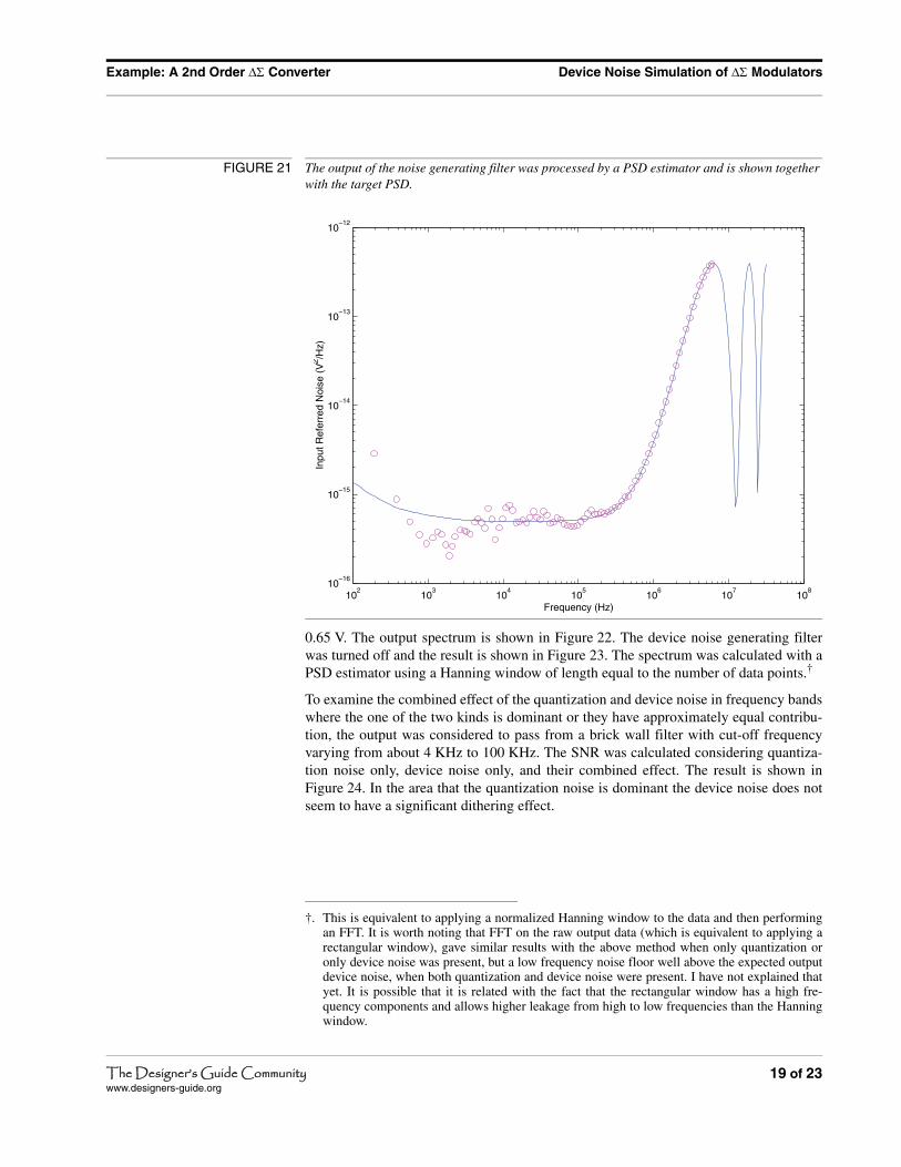
The obtained discrete time filter was fed with white noise and the output was processedwith a PSD estimator. The result is shown in Figure 21 together with the target PSD.Very good agreement is observed at high frequencies, while at low frequencies the esti-mation is impaired by the finite observation time.
The second order converter of Figure 5 was implemented in difference equation form inVerilog-A and simulated with SpectreRF. A digital filter was also included in the Ver-ilog-A file and noise with PSD equal to the input referred noise was injected at the inputtogether with a sinusoid of frequency fsig = 3.051757 KHz = fs/4096 and amplitude
†. The pole-residue filter realization is Joel Phillips’ suggestion.
FIGURE 20 Fit of a discrete time transfer function to the numerical data obtained from SpectreRF ( ).
10−2
100
102
104
106
108
10−16
10−15
10−14
10−13
10−12
Frequency (Hz)
Inpu
t ref
erre
d no
ise
(V2 /H
z)
y k( ) c xi k( )ri w k( )+
i 1=
n
∑=
xi k 1+( ) pixi k( ) w k( )+= i 1 … n, ,=
18 of 23 The Designer’s Guide Communitywww.designers-guide.org
Example: A 2nd Order ΔΣ Converter Device Noise Simulation of ΔΣ Modulators
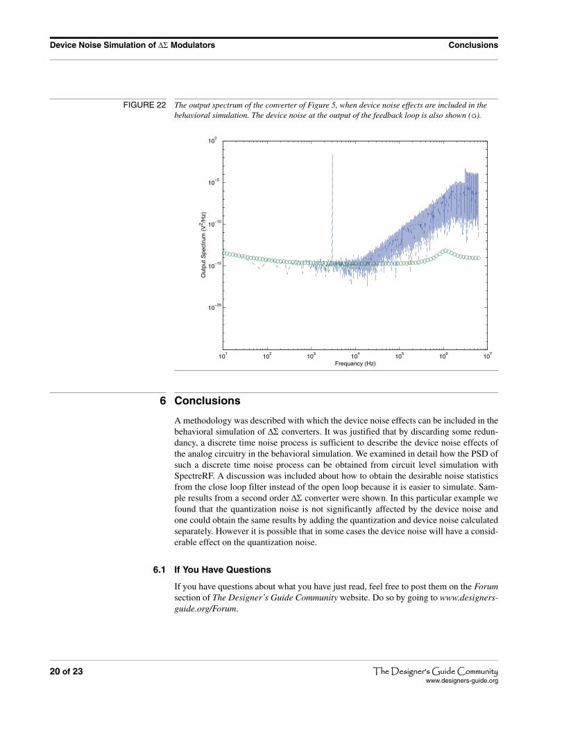
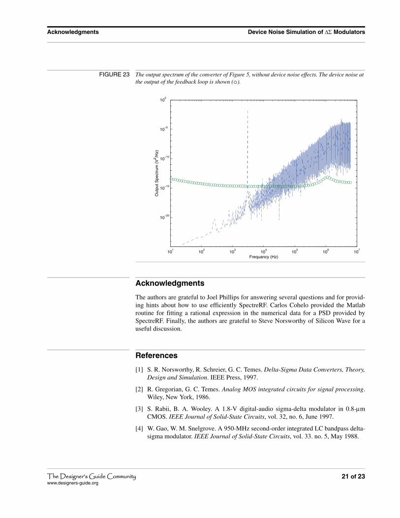
0.65 V. The output spectrum is shown in Figure 22. The device noise generating filterwas turned off and the result is shown in Figure 23. The spectrum was calculated with aPSD estimator using a Hanning window of length equal to the number of data points.†
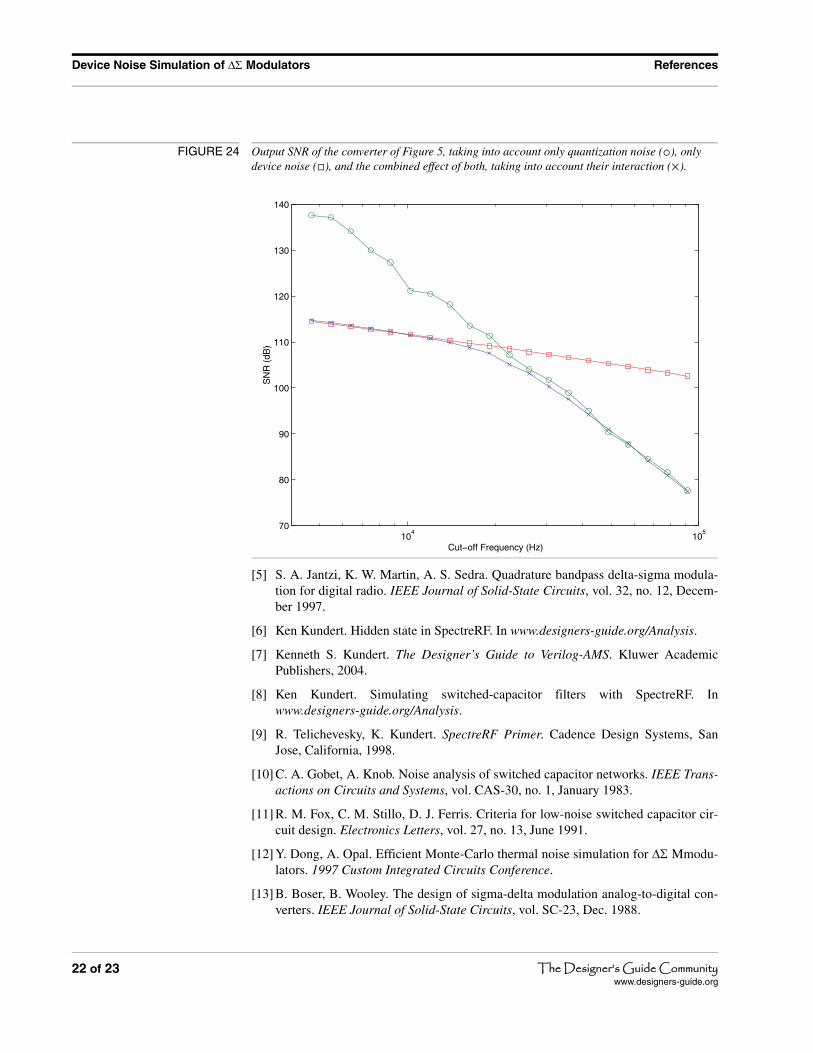
To examine the combined effect of the quantization and device noise in frequency bandswhere the one of the two kinds is dominant or they have approximately equal contribu-tion, the output was considered to pass from a brick wall filter with cut-off frequencyvarying from about 4 KHz to 100 KHz. The SNR was calculated considering quantiza-tion noise only, device noise only, and their combined effect. The result is shown inFigure 24. In the area that the quantization noise is dominant the device noise does notseem to have a significant dithering effect.
FIGURE 21 The output of the noise generating filter was processed by a PSD estimator and is shown together with the target PSD.
†. This is equivalent to applying a normalized Hanning window to the data and then performingan FFT. It is worth noting that FFT on the raw output data (which is equivalent to applying arectangular window), gave similar results with the above method when only quantization oronly device noise was present, but a low frequency noise floor well above the expected outputdevice noise, when both quantization and device noise were present. I have not explained thatyet. It is possible that it is related with the fact that the rectangular window has a high fre-quency components and allows higher leakage from high to low frequencies than the Hanningwindow.
102
103
104
105
106
107
108
10−16
10−15
10−14
10−13
10−12
Frequency (Hz)
Inpu
t Ref
erre
d N
oise
(V
2 /Hz)
19 of 23The Designer’s Guide Communitywww.designers-guide.org
Device Noise Simulation of ΔΣ Modulators Conclusions
6 Conclusions
A methodology was described with which the device noise effects can be included in thebehavioral simulation of ΔΣ converters. It was justified that by discarding some redun-dancy, a discrete time noise process is sufficient to describe the device noise effects ofthe analog circuitry in the behavioral simulation. We examined in detail how the PSD ofsuch a discrete time noise process can be obtained from circuit level simulation withSpectreRF. A discussion was included about how to obtain the desirable noise statisticsfrom the close loop filter instead of the open loop because it is easier to simulate. Sam-ple results from a second order ΔΣ converter were shown. In this particular example wefound that the quantization noise is not significantly affected by the device noise andone could obtain the same results by adding the quantization and device noise calculatedseparately. However it is possible that in some cases the device noise will have a consid-erable effect on the quantization noise.
6.1 If You Have Questions
If you have questions about what you have just read, feel free to post them on the Forumsection of The Designer’s Guide Community website. Do so by going to www.designers-guide.org/Forum.
FIGURE 22 The output spectrum of the converter of Figure 5, when device noise effects are included in the behavioral simulation. The device noise at the output of the feedback loop is also shown ( ).
101
102
103
104
105
106
107
10−20
10−15
10−10
10−5
100
Frequancy (Hz)
Out
put S
pect
rum
(V
2 /Hz)
20 of 23 The Designer’s Guide Communitywww.designers-guide.org
Acknowledgments Device Noise Simulation of ΔΣ Modulators
Acknowledgments
The authors are grateful to Joel Phillips for answering several questions and for provid-ing hints about how to use efficiently SpectreRF. Carlos Cohelo provided the Matlabroutine for fitting a rational expression in the numerical data for a PSD provided bySpectreRF. Finally, the authors are grateful to Steve Norsworthy of Silicon Wave for auseful discussion.
References
[1] S. R. Norsworthy, R. Schreier, G. C. Temes. Delta-Sigma Data Converters, Theory,Design and Simulation. IEEE Press, 1997.
[2] R. Gregorian, G. C. Temes. Analog MOS integrated circuits for signal processing.Wiley, New York, 1986.
[3] S. Rabii, B. A. Wooley. A 1.8-V digital-audio sigma-delta modulator in 0.8-μmCMOS. IEEE Journal of Solid-State Circuits, vol. 32, no. 6, June 1997.
[4] W. Gao, W. M. Snelgrove. A 950-MHz second-order integrated LC bandpass delta-sigma modulator. IEEE Journal of Solid-State Circuits, vol. 33. no. 5, May 1988.
FIGURE 23 The output spectrum of the converter of Figure 5, without device noise effects. The device noise at the output of the feedback loop is shown ( ).
101
102
103
104
105
106
107
10−20
10−15
10−10
10−5
100
Frequancy (Hz)
Out
put S
pect
rum
(V
2 /Hz)
21 of 23The Designer’s Guide Communitywww.designers-guide.org
Device Noise Simulation of ΔΣ Modulators References
[5] S. A. Jantzi, K. W. Martin, A. S. Sedra. Quadrature bandpass delta-sigma modula-tion for digital radio. IEEE Journal of Solid-State Circuits, vol. 32, no. 12, Decem-ber 1997.
[6] Ken Kundert. Hidden state in SpectreRF. In www.designers-guide.org/Analysis.
[7] Kenneth S. Kundert. The Designer’s Guide to Verilog-AMS. Kluwer AcademicPublishers, 2004.
[8] Ken Kundert. Simulating switched-capacitor filters with SpectreRF. Inwww.designers-guide.org/Analysis.
[9] R. Telichevesky, K. Kundert. SpectreRF Primer. Cadence Design Systems, SanJose, California, 1998.
[10] C. A. Gobet, A. Knob. Noise analysis of switched capacitor networks. IEEE Trans-actions on Circuits and Systems, vol. CAS-30, no. 1, January 1983.
[11] R. M. Fox, C. M. Stillo, D. J. Ferris. Criteria for low-noise switched capacitor cir-cuit design. Electronics Letters, vol. 27, no. 13, June 1991.
[12] Y. Dong, A. Opal. Efficient Monte-Carlo thermal noise simulation for ΔΣ Mmodu-lators. 1997 Custom Integrated Circuits Conference.
[13] B. Boser, B. Wooley. The design of sigma-delta modulation analog-to-digital con-verters. IEEE Journal of Solid-State Circuits, vol. SC-23, Dec. 1988.
FIGURE 24 Output SNR of the converter of Figure 5, taking into account only quantization noise ( ), only device noise ( ), and the combined effect of both, taking into account their interaction ( ).
104
105
70
80
90
100
110
120
130
140
Cut−off Frequency (Hz)
SN
R (
dB)
22 of 23 The Designer’s Guide Communitywww.designers-guide.org
References Device Noise Simulation of ΔΣ Modulators
[14] Midas Manual. Stanford University.
[15] Verilog-AMS Language Reference Manual: Analog & Mixed-Signal Extensions toVerilog HDL, version 2.1. Accellera, January 20, 2003. Available from www.accel-lera.com. An abridged version is available from www.verilog-ams.com orwww.designers-guide.org.
23 of 23The Designer’s Guide Communitywww.designers-guide.org