Design of Operational Transconductance Amplifier … of Operational Transconductance Amplifier for...
4
NEERAJ SHRIVASTAVA,GAURAV BHARGAVA,D.S AJNAR,PRAMOD KUMAR JAIN / International Journal of Engineering Research and Applications (IJERA) ISSN: 2248-9622 www.ijera.com Vol. 2, Issue 1,Jan-Feb 2012, pp.562-565 562 | P a g e Design of Operational Transconductance Amplifier for Biquad Filter Applications in 0.18μm Technology NEERAJ SHRIVASTAVA #1 , GAURAV BHARGAVA #2 , D.S AJNAR #3 , PRAMOD KUMAR JAIN #4 , #1, 2, 3, 4 Microelectronics and VLSI Design Electronics & Instrumentation Engineering department, SGSITS, Indore, M.P., India Abstract- This paper presents design concept of Operational Transconductance Amplifier (OTA). The 0.18μm CMOS process is used for design and simulation of this OTA. This OTA having a biasing current of 15.6 μA with supply voltage ±1.25 V. The design and simulation of this OTA is done using CADENCE Spectre environment with UMC 0.18 μm technology file. The simulation results of this OTA shows that the open loop gain of about 81.7 dB with UGB of 27.107 MHz. This OTA is having CMRR of 90 dB and PSRR of 106.07 dB. This OTA having Power dissipation of 62 uW and Slew Rate 2.44 V/μsec. Keywords- OTA, Cadence, CMRR, PSRR, Power Dissipation, CMOS IC Design. I. INTRODUCTION Due to recent development in VLSI technology, the size of transistors decreases and power supply also decreases. The OTA is a basic building block in most of analog circuits with linear input-output characteristics. The OTA is widely used in analog circuits such as Neural networks, Instrumentation amplifier, ADC and Filter circuits. The Operational Transconductance Amplifier (OTA) is basically similar to conventional Operational Amplifiers in which both having Differential inputs. The basic difference between OTA and conventional Operational Amplifier is that in OTA, the output is in form of current but in conventional Op-Amps, output is in form of Voltage. This paper is organized as follows. Section II describes brief description about operational Transconductance Amplifier (OTA) design. Section IV describes simulated characteristics of OTA. Section VI describes the conclusion of this paper. II. OPERATIONAL TRANSCONDUCTANCE AMPLIFIER (OTA) DESIGN Figure1 shows the schematic of Operational Transconductance Amplifier (OTA). In this OTA the supply voltage is VDD= +1.25V and VSS= -1.25V.The input AC signal is 7.49mV, 10GHz. The OTA is characterized by various parameters like Gain at dc (A V ),Unity gain bandwidth(UGB),Input common mode range (Vin (min) and Vin (max)),Load capacitance (C L ).The design parameters of this OTA are shown in below table I. There are several different OTA’s are used in which this OTA is a simple OTA with low supply voltage and high gain. The Op-amp is characterized by various parameters like open loop gain, Bandwidth, Slew Rate, Noise and etc. The performance Measures are fixed Due to Design parameters such as Transistors size, Bias current and etc. In this paper we describe design of OTA amplifier and this design is done in 0.18μm technology. Figure 1: Operational Transconductance Amplifier. TABLE I TRANSISTOR SIZE DEVICE W/L(um) PMOS Transistors NMOS Transistors 10/01 05/01
Transcript of Design of Operational Transconductance Amplifier … of Operational Transconductance Amplifier for...
NEERAJ SHRIVASTAVA,GAURAV BHARGAVA,D.S AJNAR,PRAMOD KUMAR JAIN /
International Journal of Engineering Research and Applications (IJERA) ISSN: 2248-9622
www.ijera.com Vol. 2, Issue 1,Jan-Feb 2012, pp.562-565
562 | P a g e
Design of Operational Transconductance Amplifier for Biquad Filter
Applications in 0.18μm Technology
NEERAJ SHRIVASTAVA#1
, GAURAV BHARGAVA#2
, D.S AJNAR#3
, PRAMOD KUMAR JAIN #4
,
#1, 2, 3, 4
Microelectronics and VLSI Design
Electronics & Instrumentation Engineering department, SGSITS, Indore, M.P., India
Abstract- This paper presents design concept of
Operational Transconductance Amplifier (OTA). The
0.18μm CMOS process is used for design and simulation
of this OTA. This OTA having a biasing current of 15.6
μA with supply voltage ±1.25 V. The design and simulation
of this OTA is done using CADENCE Spectre
environment with UMC 0.18 μm technology file. The
simulation results of this OTA shows that the open loop
gain of about 81.7 dB with UGB of 27.107 MHz. This
OTA is having CMRR of 90 dB and PSRR of 106.07 dB.
This OTA having Power dissipation of 62 uW and Slew
Rate 2.44 V/µsec.
Keywords- OTA, Cadence, CMRR, PSRR, Power Dissipation,
CMOS IC Design.
I. INTRODUCTION
Due to recent development in VLSI technology, the size of
transistors decreases and power supply also decreases. The
OTA is a basic building block in most of analog circuits with
linear input-output characteristics. The OTA is widely used in
analog circuits such as Neural networks, Instrumentation
amplifier, ADC and Filter circuits. The Operational
Transconductance Amplifier (OTA) is basically similar to
conventional Operational Amplifiers in which both having
Differential inputs. The basic difference between OTA and
conventional Operational Amplifier is that in OTA, the output
is in form of current but in conventional Op-Amps, output is
in form of Voltage.
This paper is organized as follows. Section II describes
brief description about operational Transconductance
Amplifier (OTA) design. Section IV describes simulated
characteristics of OTA. Section VI describes the conclusion of
this paper.
II. OPERATIONAL TRANSCONDUCTANCE
AMPLIFIER (OTA) DESIGN
Figure1 shows the schematic of Operational
Transconductance Amplifier (OTA). In this OTA the supply
voltage is VDD= +1.25V and VSS= -1.25V.The input AC
signal is 7.49mV, 10GHz. The OTA is characterized by
various parameters like Gain at dc (AV),Unity gain
bandwidth(UGB),Input common mode range (Vin (min) and
Vin (max)),Load capacitance (CL).The design parameters of
this OTA are shown in below table I.
There are several different OTA’s are used in which this
OTA is a simple OTA with low supply voltage and high gain.
The Op-amp is characterized by various parameters like open
loop gain, Bandwidth, Slew Rate, Noise and etc. The
performance Measures are fixed Due to Design parameters
such as Transistors size, Bias current and etc. In this paper we
describe design of OTA amplifier and this design is done in
0.18μm technology.
Figure 1: Operational Transconductance Amplifier.
TABLE I
TRANSISTOR SIZE
DEVICE W/L(um)
PMOS Transistors
NMOS Transistors
10/01
05/01
NEERAJ SHRIVASTAVA,GAURAV BHARGAVA,D.S AJNAR,PRAMOD KUMAR JAIN /
International Journal of Engineering Research and Applications (IJERA) ISSN: 2248-9622
www.ijera.com Vol. 2, Issue 1,Jan-Feb 2012, pp.562-565
563 | P a g e
III. SIMULATION RESULTS
The design of this Operational Transconductance Amplifier
(OTA) is done using Cadence Tool. The Simulation results are
done using Cadence Spectre Environment using UMC 0.18
μm CMOS technology. The simulation result of the OTA
shows that the open loop gain of approximately 81.7 dB. The
OTA has GBW of about 27.107 MHz. .
The Table II shows that the simulated results of the OTA. The
AC response which shows gain and phase change with
frequency is shown in figure 2. Figure 3 shows schematic for
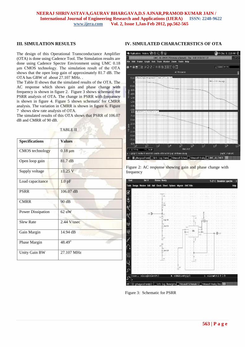
PSRR analysis of OTA. The change in PSRR with frequency
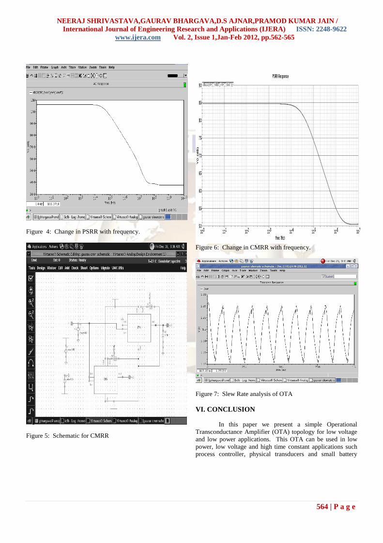
is shown in figure 4. Figure 5 shows schematic for CMRR
analysis. The variation in CMRR is shown in figure 6. Figure
7 shows slew rate analysis of OTA.
The simulated results of this OTA shows that PSRR of 106.07
dB and CMRR of 90 dB.
TABLE II
IV. SIMULATED CHARACTERSTICS OF OTA
Figure 2: AC response showing gain and phase change with
frequency
Figure 3: Schematic for PSRR
Specifications Values
CMOS technology 0.18 μm
Open loop gain 81.7 dB
Supply voltage ±1.25 V
Load capacitance 1.0 pF
PSRR 106.07 dB
CMRR 90 dB
Power Dissipation 62 uW
Slew Rate 2.44 V/usec
Gain Margin 14.94 dB
Phase Margin 48.49o
Unity Gain BW 27.107 MHz
NEERAJ SHRIVASTAVA,GAURAV BHARGAVA,D.S AJNAR,PRAMOD KUMAR JAIN /
International Journal of Engineering Research and Applications (IJERA) ISSN: 2248-9622
www.ijera.com Vol. 2, Issue 1,Jan-Feb 2012, pp.562-565
564 | P a g e
Figure 4: Change in PSRR with frequency.
Figure 5: Schematic for CMRR
Figure 6: Change in CMRR with frequency.
Figure 7: Slew Rate analysis of OTA
VI. CONCLUSION
In this paper we present a simple Operational
Transconductance Amplifier (OTA) topology for low voltage
and low power applications. This OTA can be used in low
power, low voltage and high time constant applications such
process controller, physical transducers and small battery
NEERAJ SHRIVASTAVA,GAURAV BHARGAVA,D.S AJNAR,PRAMOD KUMAR JAIN /
International Journal of Engineering Research and Applications (IJERA) ISSN: 2248-9622
www.ijera.com Vol. 2, Issue 1,Jan-Feb 2012, pp.562-565
565 | P a g e
operated devices. This work can be used in biquad filter
design, ADC design and instrumentation amplifiers because of
its high gain, high CMRR and low power consumption.
VII. REFERENCES
[1] J. H. Botma, R.F. Wassenaar, R. J. Wiegerink, “A low
voltage CMOS Op Amp with a rail-to-rail constant-
gm input stage and a class AB rail-to-rail output stage”,
IEEE 1993 ISCAS, Chicago, pp.1314-1317.
[2] Paul R. Gray, Paul L.Hurst, Stephan H.Lewis and Robort
G.Mayer “Analysis and design of analog integrated
circuits”,Forth Edition, John Wiley & sons, inc.2001,
pp.425-439.
[3] Adel S. Sedra, Kenneth C.Smith “Microelectronic
Circuits”, Oxford university press, Fourth
edition ,2002,pp.89-91.
[4] Jin Tao Li, Sio Hang Pun, Peng Un Mak and Mang I Vai
“Analysis of Op-Amp Power-Supply Current Sensing
Current-Mode Instrumentation Amplifier for Biosignal
Acquisition System”,IEEE conference,August-
2008,pp.2295-2298.
[5] Y. Tsividis, Operation and Modeling of the MOS
Transistor, 2nd ed. Boston, MA: McGraw-Hill, 1998.
[6] D. A. Johns and K. Martin, Analog Integrated Circuit
Design. New York: Wiley, 1997.
[7] Phillip E. Allen and Douglas R. Holberg “CMOS analog
circuit design” ,second edition, Oxford university press,
2007,pp. 269-274.
Authors Profile:
NEERAJ SHRIVASTAVA
He has received the B.E. degree in Electronics
and Telecommunication Engineering from Chhattisgarh
Swami Vivekanand Technical University, Bhilai in 2010 .He
is currently pursuing M.Tech degree in Microelectronics and
VLSI Design from S.G.S.I.T.S. Indore, India.
GAURAV BHARGAVA
He has received the B.E. degree in Electronics
and Communication Engineering from Rajiv Gandhi
Technical University Bhopal, in 2009. He is currently
pursuing M.Tech degree in Microelectronics and VLSI Design
from S.G.S.I.T.S. Indore, Indore.
D.S AJNAR
He has received the B.E. degree in
Electronics and Communication Engineering from S.G.S.I.T.S.
affiliated to D.A.V.V.University (Formerly known as
University Of Indore), Indore, India in 1993 and M.E. Degree
in Digital Techniques & Instrumentation Engineering from
Rajiv Gandhi Technical University Bhopal, India in 2000. He
has been in teaching and Research Profession since 1995. He
is now working as Associate Professor in Department of
Electronics & Instrumentation Engineering, S.G.S.I.T.S.,
Indore, India. His interest of research is in designing of
Analog filter and Current Conveyer.
Er. PRAMOD KUMAR JAIN
He has received the B.E. degree in
Electronics and Communication Engineering from D.A.V.V.
University (Formerly known as University Of Indore), Indore,
India in 1987 and M.E. Degree in Digital Techniques &
Instrumentation Engineering from D.A.V.V. University,
Indore, India in 1993. He has been in teaching and Research
Profession since 1988. He is now working as Associate
Professor in Department of Electronics & Instrumentation
Engineering, S.G.S.I.T.S., Indore. He has also worked as a
computer Engineer. His interest of research is in Analog and
digital system design.