Design of Cascaded WLNA based on Transistor Biasing ... calculated by using stability factor K and...
5
International Research Journal of Engineering and Technology (IRJET) e-ISSN: 2395 -0056 Volume: 03 Issue: 04 | Apr-2016 www.irjet.net p-ISSN: 2395-0072 © 2016, IRJET ISO 9001:2008 Certified Journal Page 317 Design of Cascaded WLNA based on Transistor Biasing &Voltage Divider Biasing Technique for Multiple Application Nikita. R. Varma 1 , Prof. Bhushan. R. Vidhale 2 1 Dept. Electronics & Telecomm, G.H. Raisoni college of Engg., Maharashtra, India 2 Dept. Electronics & Telecomm, G.H. Raisoni college of Engg., Maharashtra, India ---------------------------------------------------------------------***--------------------------------------------------------------------- Abstract - NOW A days the demand for high speed wireless communication systems is growing. There are several existing solutions which give high frequency wideband amplifiers in CMOS technology. Complementary metal oxide semiconductor has become a competitive technology for implementation of radio transceiver for various wireless communication system due to technology’s advantage for low cost low power consumption. In wireless communication system, the LNA plays an important role as because in the first stage receiver gives signal amplification and noise immunity. With the assistance of the ADS simulation software and the adoption of TSMC 0.13μm CMOS process, a promising LNA circuit is implemented. Using LNA, the effect of noise from subsequent stage of the receive chain is reduced by the gain of the LNA.in this for the designing of LNA the different topologies is used, proper matching is done also for the proper biasing different biasing circuit is used. Key Words: Gain, Impedance Matching, Noise Figure, Power Consumption, Wideband, Reflection Coefficient, Stability, s-parameter. 1. INTRODUCTION With rapidly increasing technology, wireless communication is evidencing introduction of various communication standards. Due to rapidly increasing applications for wireless communication systems demands for wideband multiple standard wireless system is also get increased. Therefore, it is desirable to develop a single mobile terminal compatible with several standards. With the growth of technology its need’s a Multiband/wideband receiver that would support multiple standard applications. The Low noise amplifier is the chief component of any RF receiver design in Wireless communication systems. Low Noise Amplifier is an electronic amplifier which is used to amplify possibly very weak signals also LNA is placed at the front end of a receiver. LNA’s performance is results in the overall receiver performance. The main function of low noise amplifier (LNA) is to amplify low level signals and also to maintain a very low noise. The main function of low noise amplifier is to amplify the received signal without introducing any noise, hence eliminate channel interference. Low Noise Amplifier (LNA) plays an important role in the receiver designs. At the first stage of RF receiver LNA is located and it has dominant effect on the noise performance of the overall system. As the LNA amplifies extremely low signals without adding any noise, thus the Signal-to-Noise Ratio (SNR) of the system is preserved. In LNA design, it is necessary that LNA results in high gain, low noise figure, stability, good input and output matching. 2. LNA DESIGN PROCEDURE In every communication receiver, LNA is a prime component of the system design. LNA is located at front end to reduce the losses in feed line. The received signal is first amplified by LNA circuit and the processed further through various stage of receiver. Figure1.1: Generic amplifier block diagram Figure 1.1 stages of LNA in which the signal is captured by antenna as input it is fed to the input matching network. The input matching manages matching of the input impedance. After input matching the signal is further pass through the various stages of LNA also for proper biasing different biasing technique is used. The transistor unit processes the signal and finally with proper matching at output side the amplified signal is obtained. Low noise amplifiers (LNAs) play a key role in performance of radio receiver. The success results of a receiver’s design are measured in multiple dimensions: receiver sensitivity, selectivity, and proclivity to reception errors.
Transcript of Design of Cascaded WLNA based on Transistor Biasing ... calculated by using stability factor K and...
International Research Journal of Engineering and Technology (IRJET) e-ISSN: 2395 -0056
Volume: 03 Issue: 04 | Apr-2016 www.irjet.net p-ISSN: 2395-0072
© 2016, IRJET ISO 9001:2008 Certified Journal Page 317
Design of Cascaded WLNA based on Transistor Biasing &Voltage
Divider Biasing Technique for Multiple Application
Nikita. R. Varma 1, Prof. Bhushan. R. Vidhale2
1 Dept. Electronics & Telecomm, G.H. Raisoni college of Engg., Maharashtra, India 2 Dept. Electronics & Telecomm, G.H. Raisoni college of Engg., Maharashtra, India
---------------------------------------------------------------------***---------------------------------------------------------------------
Abstract - NOW A days the demand for high speed wireless communication systems is growing. There are several existing solutions which give high frequency wideband amplifiers in CMOS technology. Complementary metal oxide semiconductor has become a competitive technology for implementation of radio transceiver for various wireless communication system due to technology’s advantage for low cost low power consumption. In wireless communication system, the LNA plays an important role as because in the first stage receiver gives signal amplification and noise immunity. With the assistance of the ADS simulation software and the adoption of TSMC 0.13µm CMOS process, a promising LNA circuit is implemented. Using LNA, the effect of noise from subsequent stage of the receive chain is reduced by the gain of the LNA.in this for the designing of LNA the different topologies is used, proper matching is done also for the proper biasing different biasing circuit is used.
Key Words: Gain, Impedance Matching, Noise Figure, Power Consumption, Wideband, Reflection Coefficient, Stability, s-parameter.
1. INTRODUCTION
With rapidly increasing technology, wireless communication is evidencing introduction of various communication standards. Due to rapidly increasing applications for wireless communication systems demands for wideband multiple standard wireless system is also get increased. Therefore, it is desirable to develop a single mobile terminal compatible with several standards. With the growth of technology its need’s a Multiband/wideband receiver that would support multiple standard applications. The Low noise amplifier is the chief component of any RF receiver design in Wireless communication systems. Low Noise Amplifier is an electronic amplifier which is used to amplify possibly very weak signals also LNA is placed at the front end of a receiver. LNA’s performance is results in the overall receiver performance.
The main function of low noise amplifier (LNA) is to amplify low level signals and also to maintain a very low noise. The main function of low noise amplifier is to amplify the received signal without introducing any noise, hence
eliminate channel interference. Low Noise Amplifier (LNA) plays an important role in the receiver designs. At the first stage of RF receiver LNA is located and it has dominant effect on the noise performance of the overall system. As the LNA amplifies extremely low signals without adding any noise, thus the Signal-to-Noise Ratio (SNR) of the system is preserved. In LNA design, it is necessary that LNA results in high gain, low noise figure, stability, good input and output matching.
2. LNA DESIGN PROCEDURE
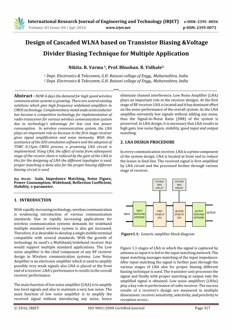
In every communication receiver, LNA is a prime component of the system design. LNA is located at front end to reduce the losses in feed line. The received signal is first amplified by LNA circuit and the processed further through various stage of receiver.
Figure1.1: Generic amplifier block diagram
Figure 1.1 stages of LNA in which the signal is captured by antenna as input it is fed to the input matching network. The input matching manages matching of the input impedance. After input matching the signal is further pass through the various stages of LNA also for proper biasing different biasing technique is used. The transistor unit processes the signal and finally with proper matching at output side the amplified signal is obtained. Low noise amplifiers (LNAs) play a key role in performance of radio receiver. The success results of a receiver’s design are measured in multiple dimensions: receiver sensitivity, selectivity, and proclivity to reception errors.
International Research Journal of Engineering and Technology (IRJET) e-ISSN: 2395 -0056
Volume: 03 Issue: 04 | Apr-2016 www.irjet.net p-ISSN: 2395-0072
© 2016, IRJET ISO 9001:2008 Certified Journal Page 318
3. LNA DESIGN PARAMETERS
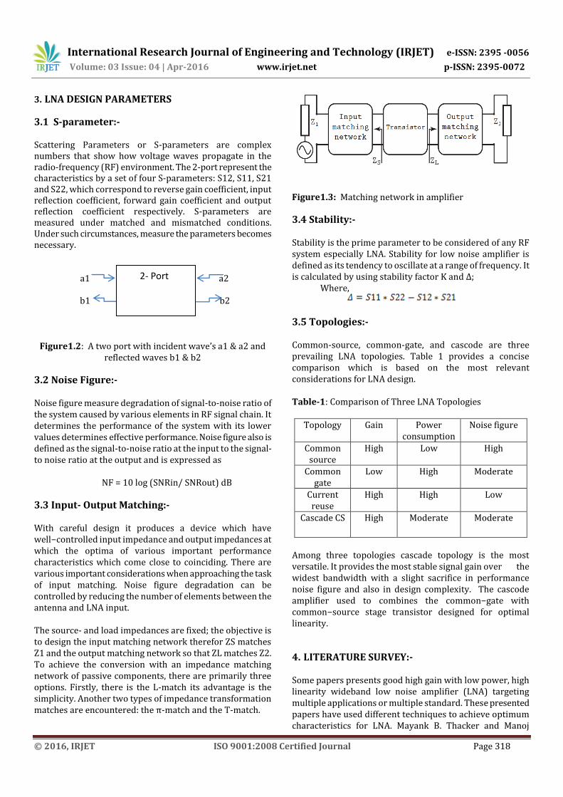
3.1 S-parameter:-
Scattering Parameters or S-parameters are complex numbers that show how voltage waves propagate in the radio-frequency (RF) environment. The 2-port represent the characteristics by a set of four S-parameters: S12, S11, S21 and S22, which correspond to reverse gain coefficient, input reflection coefficient, forward gain coefficient and output reflection coefficient respectively. S-parameters are measured under matched and mismatched conditions. Under such circumstances, measure the parameters becomes necessary. a1 a2
b1 b2
Figure1.2: A two port with incident wave’s a1 & a2 and reflected waves b1 & b2
3.2 Noise Figure:- Noise figure measure degradation of signal-to-noise ratio of the system caused by various elements in RF signal chain. It determines the performance of the system with its lower values determines effective performance. Noise figure also is defined as the signal-to-noise ratio at the input to the signal-to noise ratio at the output and is expressed as
NF = 10 log (SNRin/ SNRout) dB
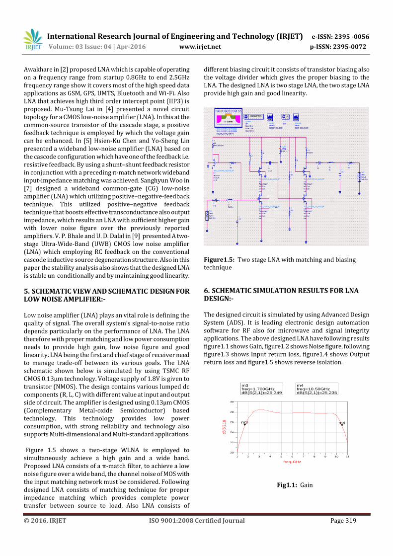
3.3 Input- Output Matching:- With careful design it produces a device which have well−controlled input impedance and output impedances at which the optima of various important performance characteristics which come close to coinciding. There are various important considerations when approaching the task of input matching. Noise figure degradation can be controlled by reducing the number of elements between the antenna and LNA input. The source- and load impedances are fixed; the objective is to design the input matching network therefor ZS matches Z1 and the output matching network so that ZL matches Z2. To achieve the conversion with an impedance matching network of passive components, there are primarily three options. Firstly, there is the L-match its advantage is the simplicity. Another two types of impedance transformation matches are encountered: the π-match and the T-match.
Figure1.3: Matching network in amplifier
3.4 Stability:-
Stability is the prime parameter to be considered of any RF system especially LNA. Stability for low noise amplifier is defined as its tendency to oscillate at a range of frequency. It is calculated by using stability factor K and Δ;
Where,
3.5 Topologies:-
Common-source, common-gate, and cascode are three prevailing LNA topologies. Table 1 provides a concise comparison which is based on the most relevant considerations for LNA design.
Table-1: Comparison of Three LNA Topologies
Topology Gain Power consumption
Noise figure
Common source
High Low High
Common gate
Low High Moderate
Current reuse
High High Low
Cascade CS High Moderate Moderate
Among three topologies cascade topology is the most versatile. It provides the most stable signal gain over the widest bandwidth with a slight sacrifice in performance noise figure and also in design complexity. The cascode amplifier used to combines the common−gate with common−source stage transistor designed for optimal linearity.
4. LITERATURE SURVEY:-
Some papers presents good high gain with low power, high linearity wideband low noise amplifier (LNA) targeting multiple applications or multiple standard. These presented papers have used different techniques to achieve optimum characteristics for LNA. Mayank B. Thacker and Manoj
2- Port
International Research Journal of Engineering and Technology (IRJET) e-ISSN: 2395 -0056
Volume: 03 Issue: 04 | Apr-2016 www.irjet.net p-ISSN: 2395-0072
© 2016, IRJET ISO 9001:2008 Certified Journal Page 319
Awakhare in [2] proposed LNA which is capable of operating on a frequency range from startup 0.8GHz to end 2.5GHz frequency range show it covers most of the high speed data applications as GSM, GPS, UMTS, Bluetooth and Wi-Fi. Also LNA that achieves high third order intercept point (IIP3) is proposed. Mu-Tsung Lai in [4] presented a novel circuit topology for a CMOS low-noise amplifier (LNA). In this at the common-source transistor of the cascade stage, a positive feedback technique is employed by which the voltage gain can be enhanced. In [5] Hsien-Ku Chen and Yo-Sheng Lin presented a wideband low-noise amplifier (LNA) based on the cascode configuration which have one of the feedback i.e. resistive feedback. By using a shunt–shunt feedback resistor in conjunction with a preceding π-match network wideband input-impedance matching was achieved. Sanghyun Woo in [7] designed a wideband common-gate (CG) low-noise amplifier (LNA) which utilizing positive–negative-feedback technique. This utilized positive–negative feedback technique that boosts effective transconductance also output impedance, which results an LNA with sufficient higher gain with lower noise figure over the previously reported amplifiers. V. P. Bhale and U. D. Dalal in [9] presented A two-stage Ultra-Wide-Band (UWB) CMOS low noise amplifier (LNA) which employing RC feedback on the conventional cascode inductive source degeneration structure. Also in this paper the stability analysis also shows that the designed LNA is stable un-conditionally and by maintaining good linearity.
5. SCHEMATIC VIEW AND SCHEMATIC DESIGN FOR LOW NOISE AMPLIFIER:-
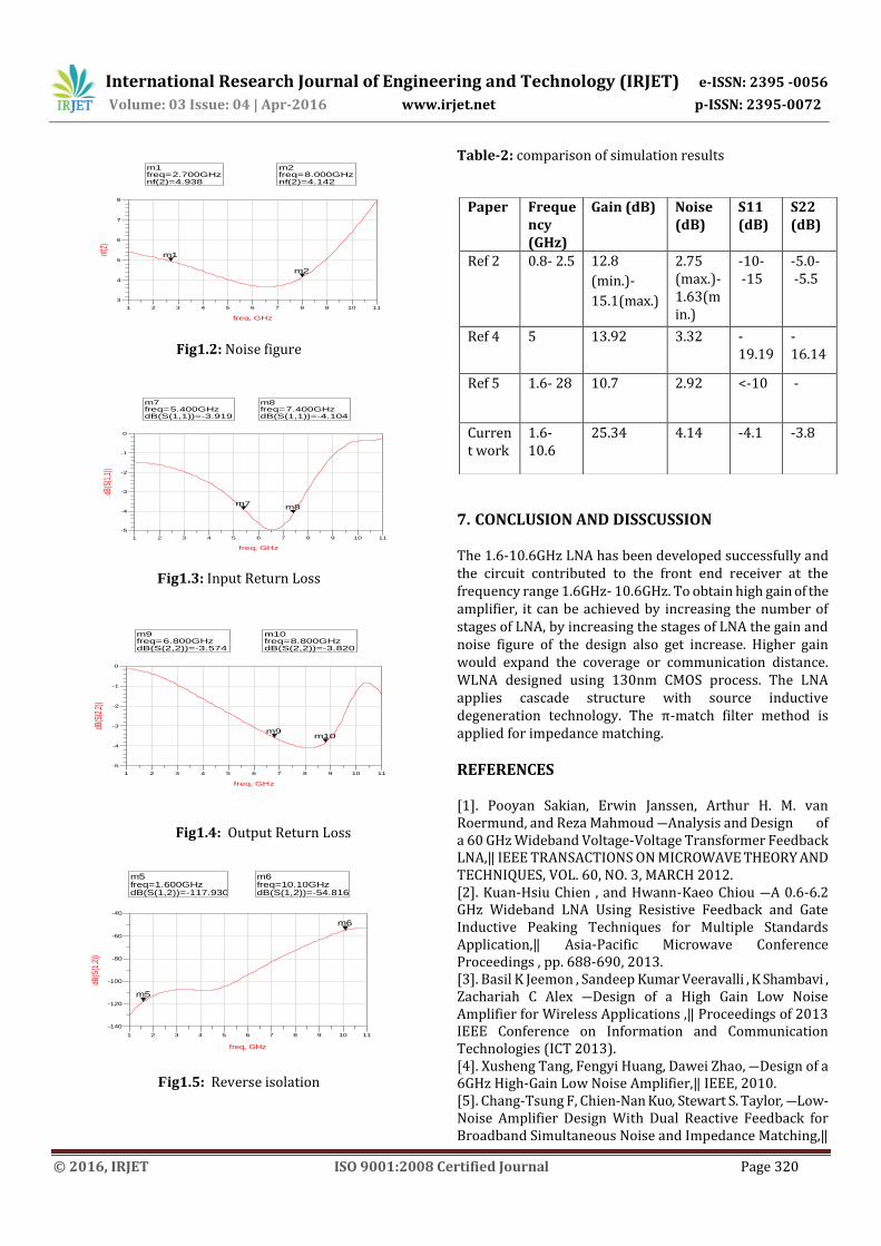
Low noise amplifier (LNA) plays an vital role is defining the quality of signal. The overall system’s signal-to-noise ratio depends particularly on the performance of LNA. The LNA therefore with proper matching and low power consumption needs to provide high gain, low noise figure and good linearity. LNA being the first and chief stage of receiver need to manage trade-off between its various goals. The LNA schematic shown below is simulated by using TSMC RF CMOS 0.13μm technology. Voltage supply of 1.8V is given to transistor (NMOS). The design contains various lumped dc components (R, L, C) with different value at input and output side of circuit. The amplifier is designed using 0.13μm CMOS (Complementary Metal-oxide Semiconductor) based technology. This technology provides low power consumption, with strong reliability and technology also supports Multi-dimensional and Multi-standard applications.
Figure 1.5 shows a two-stage WLNA is employed to simultaneously achieve a high gain and a wide band. Proposed LNA consists of a π-match filter, to achieve a low noise figure over a wide band, the channel noise of MOS with the input matching network must be considered. Following designed LNA consists of matching technique for proper impedance matching which provides complete power transfer between source to load. Also LNA consists of
different biasing circuit it consists of transistor biasing also the voltage divider which gives the proper biasing to the LNA. The designed LNA is two stage LNA, the two stage LNA provide high gain and good linearity.
Figure1.5: Two stage LNA with matching and biasing technique
6. SCHEMATIC SIMULATION RESULTS FOR LNA DESIGN:-
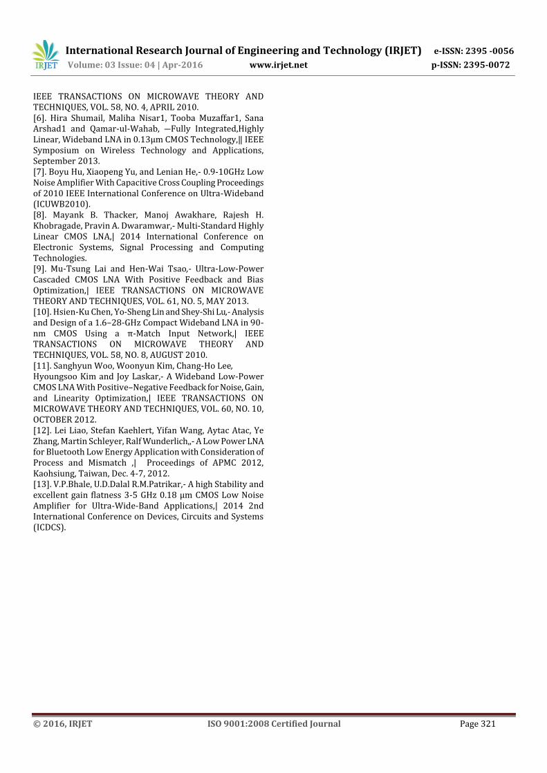
The designed circuit is simulated by using Advanced Design System (ADS). It is leading electronic design automation software for RF also for microwave and signal integrity applications. The above designed LNA have following results figure1.1 shows Gain, figure1.2 shows Noise figure, following figure1.3 shows Input return loss, figure1.4 shows Output return loss and figure1.5 shows reverse isolation.
Fig1.1: Gain
2 3 4 5 6 7 8 9 101 11
22
24
26
28
20
30
freq, GHz
dB(S
(2,1
))
Readout
m3
Readout
m4
m3freq=dB(S(2,1))=25.349
1.700GHzm4freq=dB(S(2,1))=25.235
10.50GHz
International Research Journal of Engineering and Technology (IRJET) e-ISSN: 2395 -0056
Volume: 03 Issue: 04 | Apr-2016 www.irjet.net p-ISSN: 2395-0072
© 2016, IRJET ISO 9001:2008 Certified Journal Page 320
Fig1.2: Noise figure
Fig1.3: Input Return Loss
Fig1.4: Output Return Loss
Fig1.5: Reverse isolation
Table-2: comparison of simulation results
7. CONCLUSION AND DISSCUSSION
The 1.6-10.6GHz LNA has been developed successfully and the circuit contributed to the front end receiver at the frequency range 1.6GHz- 10.6GHz. To obtain high gain of the amplifier, it can be achieved by increasing the number of stages of LNA, by increasing the stages of LNA the gain and noise figure of the design also get increase. Higher gain would expand the coverage or communication distance. WLNA designed using 130nm CMOS process. The LNA applies cascade structure with source inductive degeneration technology. The π-match filter method is applied for impedance matching.
REFERENCES
[1]. Pooyan Sakian, Erwin Janssen, Arthur H. M. van Roermund, and Reza Mahmoud ―Analysis and Design of a 60 GHz Wideband Voltage-Voltage Transformer Feedback LNA,‖ IEEE TRANSACTIONS ON MICROWAVE THEORY AND TECHNIQUES, VOL. 60, NO. 3, MARCH 2012. [2]. Kuan-Hsiu Chien , and Hwann-Kaeo Chiou ―A 0.6-6.2 GHz Wideband LNA Using Resistive Feedback and Gate Inductive Peaking Techniques for Multiple Standards Application,‖ Asia-Pacific Microwave Conference Proceedings , pp. 688-690, 2013. [3]. Basil K Jeemon , Sandeep Kumar Veeravalli , K Shambavi , Zachariah C Alex ―Design of a High Gain Low Noise Amplifier for Wireless Applications ,‖ Proceedings of 2013 IEEE Conference on Information and Communication Technologies (ICT 2013). [4]. Xusheng Tang, Fengyi Huang, Dawei Zhao, ―Design of a 6GHz High-Gain Low Noise Amplifier,‖ IEEE, 2010. [5]. Chang-Tsung F, Chien-Nan Kuo, Stewart S. Taylor, ―Low-Noise Amplifier Design With Dual Reactive Feedback for Broadband Simultaneous Noise and Impedance Matching,‖
Paper Frequency (GHz)
Gain (dB) Noise (dB)
S11 (dB)
S22 (dB)
Ref 2 0.8- 2.5 12.8
(min.)-
15.1(max.)
2.75 (max.)- 1.63(min.)
-10- -15
-5.0- -5.5
Ref 4 5 13.92 3.32 -19.19
-16.14
Ref 5 1.6- 28 10.7 2.92 <-10 -
Current work
1.6-10.6
25.34 4.14 -4.1 -3.8
2 3 4 5 6 7 8 9 101 11
4
5
6
7
3
8
freq, GHz
nf(2
)
2.700G4.938
m1
8.000G4.142
m2
m1freq=nf(2)=4.938
2.700GHzm2freq=nf(2)=4.142
8.000GHz
2 3 4 5 6 7 8 9 101 11
-4
-3
-2
-1
-5
0
freq, GHz
dB(S
(1,1
))
Readout
m7
Readout
m8
m7freq=dB(S(1,1))=-3.919
5.400GHzm8freq=dB(S(1,1))=-4.104
7.400GHz
2 3 4 5 6 7 8 9 101 11
-4
-3
-2
-1
-5
0
freq, GHz
dB(S
(2,2
))
Readout
m9
Readout
m10
m9freq=dB(S(2,2))=-3.574
6.800GHzm10freq=dB(S(2,2))=-3.820
8.800GHz
2 3 4 5 6 7 8 9 101 11
-120
-100
-80
-60
-140
-40
freq, GHz
dB(S
(1,2
))
Readout
m5
Readout
m6
m5freq=dB(S(1,2))=-117.930
1.600GHzm6freq=dB(S(1,2))=-54.816
10.10GHz
International Research Journal of Engineering and Technology (IRJET) e-ISSN: 2395 -0056
Volume: 03 Issue: 04 | Apr-2016 www.irjet.net p-ISSN: 2395-0072
© 2016, IRJET ISO 9001:2008 Certified Journal Page 321
IEEE TRANSACTIONS ON MICROWAVE THEORY AND TECHNIQUES, VOL. 58, NO. 4, APRIL 2010. [6]. Hira Shumail, Maliha Nisar1, Tooba Muzaffar1, Sana Arshad1 and Qamar-ul-Wahab, ―Fully Integrated,Highly Linear, Wideband LNA in 0.13μm CMOS Technology,‖ IEEE Symposium on Wireless Technology and Applications, September 2013. [7]. Boyu Hu, Xiaopeng Yu, and Lenian He,- 0.9-10GHz Low Noise Amplifier With Capacitive Cross Coupling Proceedings of 2010 IEEE International Conference on Ultra-Wideband (ICUWB2010). [8]. Mayank B. Thacker, Manoj Awakhare, Rajesh H. Khobragade, Pravin A. Dwaramwar,- Multi-Standard Highly Linear CMOS LNA,| 2014 International Conference on Electronic Systems, Signal Processing and Computing Technologies. [9]. Mu-Tsung Lai and Hen-Wai Tsao,- Ultra-Low-Power Cascaded CMOS LNA With Positive Feedback and Bias Optimization,| IEEE TRANSACTIONS ON MICROWAVE THEORY AND TECHNIQUES, VOL. 61, NO. 5, MAY 2013. [10]. Hsien-Ku Chen, Yo-Sheng Lin and Shey-Shi Lu,- Analysis and Design of a 1.6–28-GHz Compact Wideband LNA in 90-nm CMOS Using a π-Match Input Network,| IEEE TRANSACTIONS ON MICROWAVE THEORY AND TECHNIQUES, VOL. 58, NO. 8, AUGUST 2010. [11]. Sanghyun Woo, Woonyun Kim, Chang-Ho Lee, Hyoungsoo Kim and Joy Laskar,- A Wideband Low-Power CMOS LNA With Positive–Negative Feedback for Noise, Gain, and Linearity Optimization,| IEEE TRANSACTIONS ON MICROWAVE THEORY AND TECHNIQUES, VOL. 60, NO. 10, OCTOBER 2012. [12]. Lei Liao, Stefan Kaehlert, Yifan Wang, Aytac Atac, Ye Zhang, Martin Schleyer, Ralf Wunderlich,,- A Low Power LNA for Bluetooth Low Energy Application with Consideration of Process and Mismatch ,| Proceedings of APMC 2012, Kaohsiung, Taiwan, Dec. 4-7, 2012. [13]. V.P.Bhale, U.D.Dalal R.M.Patrikar,- A high Stability and excellent gain flatness 3-5 GHz 0.18 μm CMOS Low Noise Amplifier for Ultra-Wide-Band Applications,| 2014 2nd International Conference on Devices, Circuits and Systems (ICDCS).