Department of Computer Engineering | Sharif University of ...
16
ﺗﺤﻠﻴﻞ ﭼﻨﺪ ﻣﺴﺌﻠﻪ ﻧﻤﻮﻧﻪ ﻣﺴﺎﺋﻠﻲ ﻛﻪ ﺟﻬﺖ ﻧﻤﻮﻧﻪ ﺗﺤﻠﻴﻞ ﺷﺪه اﻧﺪ ﻣﺘﻌﻠﻖ ﺑﻪ ﻛﺘﺎب زﻳﺮ ﻣﻲ ﺑﺎﺷﻨﺪ: Design of Analog CMOS Integrated Circuits Author: Behzad Razavi ISBN: 0-07-238032-2 ﺷﻤﺎره ﻧﻤﻮﻧﻪ ﻫﺎ2-9a 2-5d Chapter 2 3-15e 3-15a Chapter 3 4-18 4-3 Chapter 4 5-16b 5-11b Chapter 5 Figure 14.8 14-3 Chapter 14
Transcript of Department of Computer Engineering | Sharif University of ...
تحليل چند مسئله نمونه
:مسائلي كه جهت نمونه تحليل شده اند متعلق به كتاب زير مي باشند
Design of Analog CMOS Integrated Circuits
Author: Behzad Razavi
ISBN: 0-07-238032-2
شماره نمونه ها
2-9a 2-5d Chapter 2
3-15e 3-15a Chapter 3
4-18 4-3 Chapter 4
5-16b 5-11b Chapter 5
Figure 14.8 14-3 Chapter 14
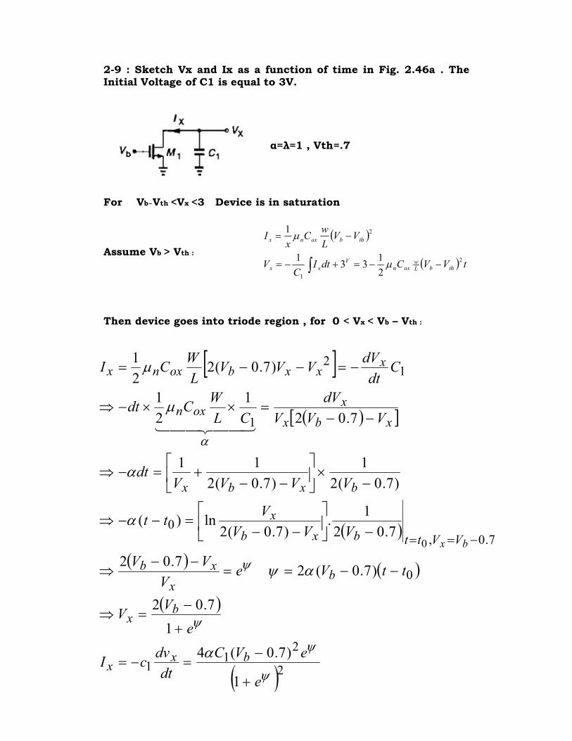
2-9 : Sketch Vx and Ix as a function of time in Fig. 2.46a . The Initial Voltage of C1 is equal to 3V.
α=λ=1 , Vth=.7
For Vb-Vth <Vx <3 Device is in saturation Assume Vb > Vth :
Then device goes into triode region , for 0 < Vx < Vb – Vth :
( )
( )∫ −−=+−=
−=
tVVCdtIC
V
VVL
wC
xI
thbLw
oxn
V
xx
thboxnx
2
1
2
2
133
1
1
µ
µ
[ ]
( )[ ]
( )
( ) ( )
( )
( )22
11
0
7.0,
0
1
12
1
)7.0(4
1
7.02
)7.0(27.02
7.02
1.
)7.0(2ln)(
)7.0(2
1
)7.0(2
11
7.02
1
2
1
)7.0(22
1
0
ψ
ψ
ψ
ψ
α
α
αψ
α
α
µ
µ
e
eVC
dt
dvcI
e
VV
ttVeV
VV
VVV
Vtt
VVVVdt
VVV
dV
CL
WCdt
Cdt
dVVVV
L
WCI
bxx
bx
bx
xb
VVttbxb
x
bxbx
xbx
xoxn
xxxboxnx
bx
+
−=−=
+
−=⇒
−−==−−
⇒
−
−−=−−⇒
−×
−−+=−⇒
−−=××−⇒
−=−−=
−==
44 344 21
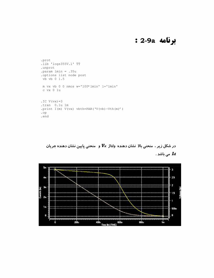
:9a-2 برنامه
.prot
.lib 'logs355V.l' TT
.unprot
.param lmin = .35u
.options list node post
vb vb 0 1.5
m vx vb 0 0 nmos w='100*lmin' l='lmin'
c vx 0 1u
.IC V(vx)=3
.tran 0.1u 1m
.print I(m) V(vx) vbth=PAR(‘V(vb)-Vth(m)’)
.op
.end
جريان و منحني پايين نشان دهنده Vxدر شكل زير ، منحني بالا نشان دهنده ولتاژ
Id باشد مي.
)1.0(
)1.0(2
1 2
L
WCg
L
WCI
oxpm
oxpx
µ
µ
−=
=
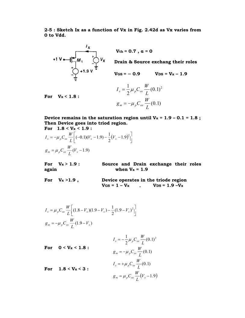
2-5 : Sketch Ix as a function of Vx in Fig. 2.42d as Vx varies from 0 to Vdd.
Vth = 0.7 , α = 0 Drain & Source exchang their roles
VGS = - 0.9 VDS = Vx – 1.9
For Vx < 1.8 :
Device remains in the saturation region until Vx = 1.9 – 0.1 = 1.8 ; Then Device goes into triod region. For 1.8 < Vx < 1.9 :
( )
)9.1(
9.12
1)9.1)(1.0(
2
−=
−−−−−=
xoxpm
xxoxpx
VL
WCg
VVL
WCI
µ
µ
For Vx > 1.9 : Source and Drain exchange their roles again when Vx = 1.9 For Vx >1.9 , Device operates in the triode region VGS = 1 – Vx , VDS = 1.9 –Vx
)9.1(
)9.1(2
1)9.1)(8.1(
2
xoxpm
xxxoxpx
VL
WCg
VVVL
WCI
−−=
−−−−=
µ
µ
For 0 < Vx < 1.8 : For 1.8 < Vx < 3 :
( )9.1
)1.0(
)1.0(
)1.0(2
1 2
−=
+=
−=
−=
xoxpm
oxpx
oxpm
oxpx
VL
WCg
L
WCI
L
WCg
L
WCI
µ
µ
µ
µ
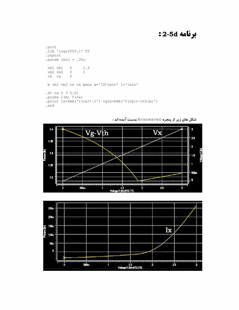
:5d-2برنامه
.prot
.lib 'logs355V.l' TT
.unprot
.param lmin = .35u
vb1 vb1 0 1.9
vb2 vb2 0 1
vx vx 0
m vb1 vb2 vx vx pmos w='10*lmin' l='lmin'
.DC vx 0 3 0.01
.probe I(m) V(vx)
.print Ix=PAR('I(vx)*-1') vgth=PAR('V(vb1)-vth(m)')
.end
: بدست آمده اند Avanwavesشكل هاي زير از پنجره
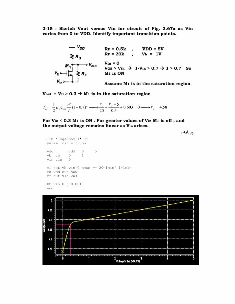
3-15 : Sketch Vout versus Vin for circuit of Fig. 3.67a as Vin varies from 0 to VDD. Identify important transition points.
RD = 0.5k , VDD = 5V RF = 20k , Vb = 1V
Vin = 0 VGS > Vth ���� 1-Vin > 0.7 ���� 1 > 0.7 So M1 is ON Assume M1 is in the saturation region
Vout = VD > 0.3 ���� M1 is in the saturation region
58.40603.05.0
5
20)7.01(
2
1 2 =→=+−
+→−= o
oo
oxnD VVV
L
WCI µ
For Vin < 0.3 M1 is ON . For greater values of Vin M1 is off , and the output voltage remains linear as Vin arises.
:برنامه .lib 'logs355V.l' TT
.param lmin = '.35u'
vdd vdd 0 5
vb vb 0 1
vin vin 0
m1 out vb vin 0 nmos w='20*lmin' l=lmin
rd vdd out 500
rf out vin 20k
.DC vin 0 5 0.001
.end
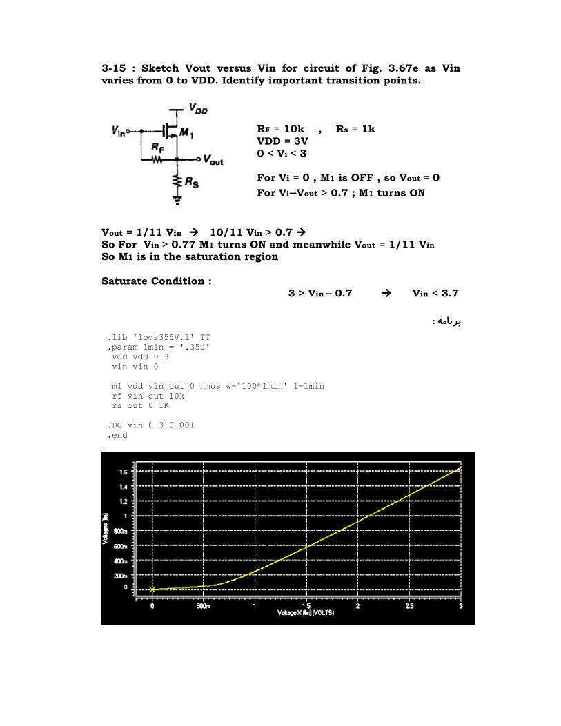
3-15 : Sketch Vout versus Vin for circuit of Fig. 3.67e as Vin varies from 0 to VDD. Identify important transition points.
RF = 10k , Rs = 1k VDD = 3V 0 < Vi < 3 For Vi = 0 , M1 is OFF , so Vout = 0
For Vi-Vout > 0.7 ; M1 turns ON
Vout = 1/11 Vin ���� 10/11 Vin > 0.7 ���� So For Vin > 0.77 M1 turns ON and meanwhile Vout = 1/11 Vin So M1 is in the saturation region
Saturate Condition :
3 > Vin – 0.7 ���� Vin < 3.7
:برنامه .lib 'logs355V.l' TT
.param lmin = '.35u'
vdd vdd 0 3
vin vin 0
m1 vdd vin out 0 nmos w='100*lmin' l=lmin
rf vin out 10k
rs out 0 1K
.DC vin 0 3 0.001
.end
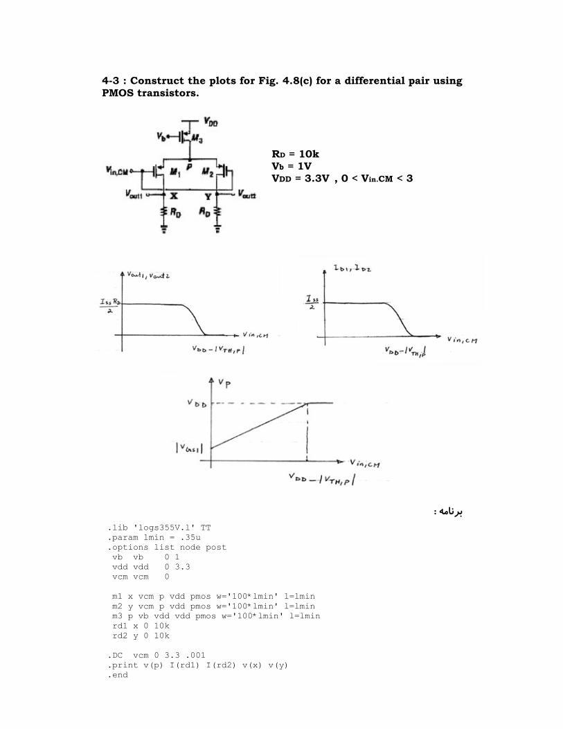
4-3 : Construct the plots for Fig. 4.8(c) for a differential pair using PMOS transistors.
RD = 10k Vb = 1V VDD = 3.3V , 0 < Vin.CM < 3
:برنامه .lib 'logs355V.l' TT
.param lmin = .35u
.options list node post
vb vb 0 1
vdd vdd 0 3.3
vcm vcm 0
m1 x vcm p vdd pmos w='100*lmin' l=lmin
m2 y vcm p vdd pmos w='100*lmin' l=lmin
m3 p vb vdd vdd pmos w='100*lmin' l=lmin
rd1 x 0 10k
rd2 y 0 10k
.DC vcm 0 3.3 .001
.print v(p) I(rd1) I(rd2) v(x) v(y)
.end
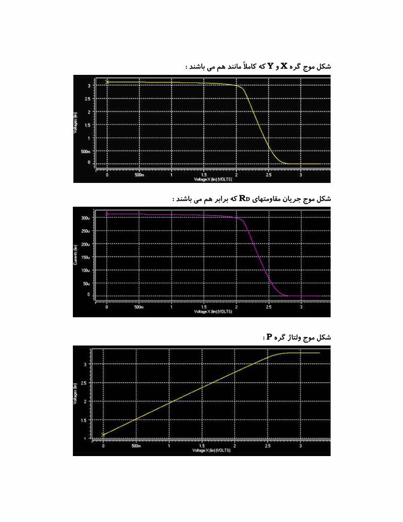
: مانند هم مي باشند كه كاملاYً و Xشكل موج گره
:كه برابر هم مي باشند RDشكل موج جريان مقاومتهاي
:Pشكل موج ولتاژ گره
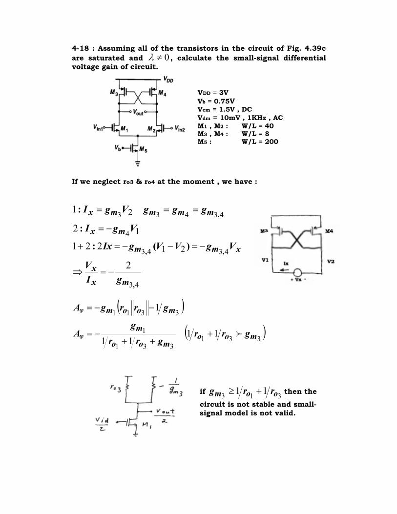
4-18 : Assuming all of the transistors in the circuit of Fig. 4.39c
are saturated and 0≠λ , calculate the small-signal differential
voltage gain of circuit. VDD = 3V
Vb = 0.75V Vcm = 1.5V , DC
Vdm = 10mV , 1KHz , AC
M1 , M2 : W/L = 40 M3 , M4 : W/L = 8 M5 : W/L = 200
If we neglect ro3 & ro4 at the moment , we have :
43
4343
4
43433
2
221
2
1
21
1
2
,
,,
,
)(:
:
:
mx
x
xmm
mx
mmmmx
gI
V
VgVVgIx
VgI
gggVgI
−=⇒
−=−−=+
−=
===
( )( )
331331
1
3311
1111
1
moomoo
mv
moomv
grrgrr
gA
grrgA
f+++
−=
−−=
if 313
11 oom rrg +≥ then the
circuit is not stable and small-
signal model is not valid.
:برنامه .prot
.lib 'logs355V.l' TT
.unprot
.param lmin = .35u
.options list node post
vdd vdd 0 3
vin1 vin1 0 sin(1.5 10m 1k 0 0 0)
vin2 vin2 0 sin(1.5 10m 1k 0 0 180)
vb vb 0 .75
m1 out1 vin1 p 0 nmos w='40*lmin' l='lmin'
m2 out2 vin2 p 0 nmos w='40*lmin' l='lmin'
m3 out1 out2 vdd vdd pmos w='8*lmin' l='lmin'
m4 out2 out1 vdd vdd pmos w='8*lmin' l='lmin'
m5 p vb 0 0 nmos w='400*lmin' l='2*lmin'
.tran .01m 10m
.op
.print I(m1) I(m2) gain = PAR('(V(out1)-V(out2))/(V(vin1)-V(vin2))')
.end
Time Current
M1
Current
M2 Gain Time
Current
M1
Current
M2 Gain
1.00000m 227.8960u 227.8960u 7.8409 11.00000m 227.8960u 227.8960u 7.8409
2.00000m 227.8960u 227.8960u 7.8409 12.00000m 227.8960u 227.8960u 7.8409
3.00000m 227.8960u 227.8960u 7.8409 13.00000m 227.8960u 227.8960u 7.8409
4.00000m 227.8960u 227.8960u 7.8409 14.00000m 227.8960u 227.8960u 7.8409
5.00000m 227.8960u 227.8960u 7.8409 15.00000m 227.8960u 227.8960u 7.8409
6.00000m 227.8960u 227.8960u 7.8409 16.00000m 227.8960u 227.8960u 7.8409
7.00000m 227.8960u 227.8960u 7.8409 17.00000m 227.8960u 227.8960u 7.8409
8.00000m 227.8960u 227.8960u 7.8409 18.00000m 227.8960u 227.8960u 7.8409
9.00000m 227.8960u 227.8960u 7.8409 19.00000m 227.8960u 227.8960u 7.8409
10.00000m 227.8960u 227.8960u 7.8409 20.00000m 227.8960u 227.8960u 7.8409
element 0:m1 0:m2 0:m3 0:m4 0:m5
model 0:nmos.3 0:nmos.3 0:pmos.3 0:pmos.3 0:nmos.12
region Saturati Saturati Saturati Saturati Saturati
id 227.8958u 227.8958u -227.8958u -227.8958u 455.7917u
ibs -607.1540a -607.1540a 2.221e-19 2.221e-19 -9.668e-19
ibd -607.9433a -607.9433a 27.5661f 27.5661f -5.7439f
vgs 970.5123m 970.5123m -1.9751 -1.9751 750.0000m
vds 495.3721m 495.3721m -1.9751 -1.9751 529.4877m
vbs -529.4877m -529.4877m 0. 0. 0.
vth 729.7303m 729.7303m -659.7967m -659.7967m 606.3598m
vdsat 217.9774m 217.9774m -1.0486 -1.0486 155.8455m
beta 8.7083m 8.7083m 304.7593u 304.7593u 40.4436m
gam eff 596.8141m 596.8141m 461.6218m 461.6218m 485.3974m
gm 1.5784m 1.5784m 271.8181u 271.8181u 5.0525m
gds 50.1484u 50.1484u 20.2977u 20.2977u 37.1273u
gmb 341.2814u 341.2814u 52.0776u 52.0776u 1.4758m
cdtot 18.0613f 18.0613f 3.7510f 3.7510f 188.2502f
cgtot 22.0237f 22.0237f 3.9351f 3.9351f 369.9977f
cstot 35.7382f 35.7382f 9.0772f 9.0772f 554.8506f
cbtot 34.0622f 34.0622f 9.2340f 9.2340f 434.6594f
cgs 16.7404f 16.7404f 3.0854f 3.0854f 293.9998f
cgd 3.9257f 3.9257f 657.6318a 657.6318a 39.0808f
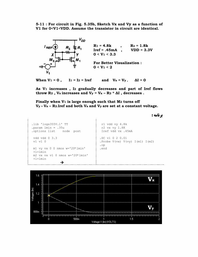
5-11 : For circuit in Fig. 5.35b, Sketch Vx and Vy as a function of V1 for 0<V1<VDD. Assume the transistor in circuit are identical.
R1 = 4.8k , R2 = 1.8k Iref = .45mA , VDD = 3.3V 0 < V1 < 3.3 For Better Visualization : 0 < V1 < 2
When V1 = 0 , I1 = I2 = Iref and Vx = Vy , ∆I = 0 As V1 increases , I2 gradually decreases and part of Iref flows throw R2 , Vx increases and Vy = Vx – R2 * ∆I , decreases . Finally when V1 is large enough such that M2 turns off Vy = Vx – R2.Iref and both Vx and Vy are set at a constant voltage.
:برنامه
r1 vdd vy 4.8k
r2 vx vy 1.8K
Iref vdd vx .45mA
.DC v1 0 2 0.01
.Probe V(vx) V(vy) I(m1) I(m2)
.op
.end
.lib 'logs355V.l' TT
.param lmin = .35u
.options list node post
vdd vdd 0 3.3
v1 v1 0
m1 vy vx 0 0 nmos w='20*lmin'
+l=lmin
m2 vx vx v1 0 nmos w='20*lmin'
+l=lmin
����
Vx
Vy

5-16 : Sketch Vx and Vy as a function of time for circuit Fig 5.40b . Assume the transistors in circuit are identical.
R1 = 47k , VDD = 3V C1 = 10pF , Iref = 300uA
M2 is ON with fixed Vx = VGS , C1 is charged with I1 until M1 turns OFF. Vy = VDD – I1R1 Where I1 goes from Iref to zero
:برنامه .lib 'logs355V.l' TT
.param lmin = .35u
.options list node post
vdd vdd 0 3
Iref vdd x 300u
m1 y x d 0 nmos w='100*lmin' l=lmin
m2 x x 0 0 nmos w='100*lmin' l=lmin
r1 vdd y 47K
c1 d 0 10p ic=0
.tran .1n 500n UIC
.Print V(x) V(y) I(r1) V(d) vgs1=PAR('v(x)-v(d)')
.op
.end
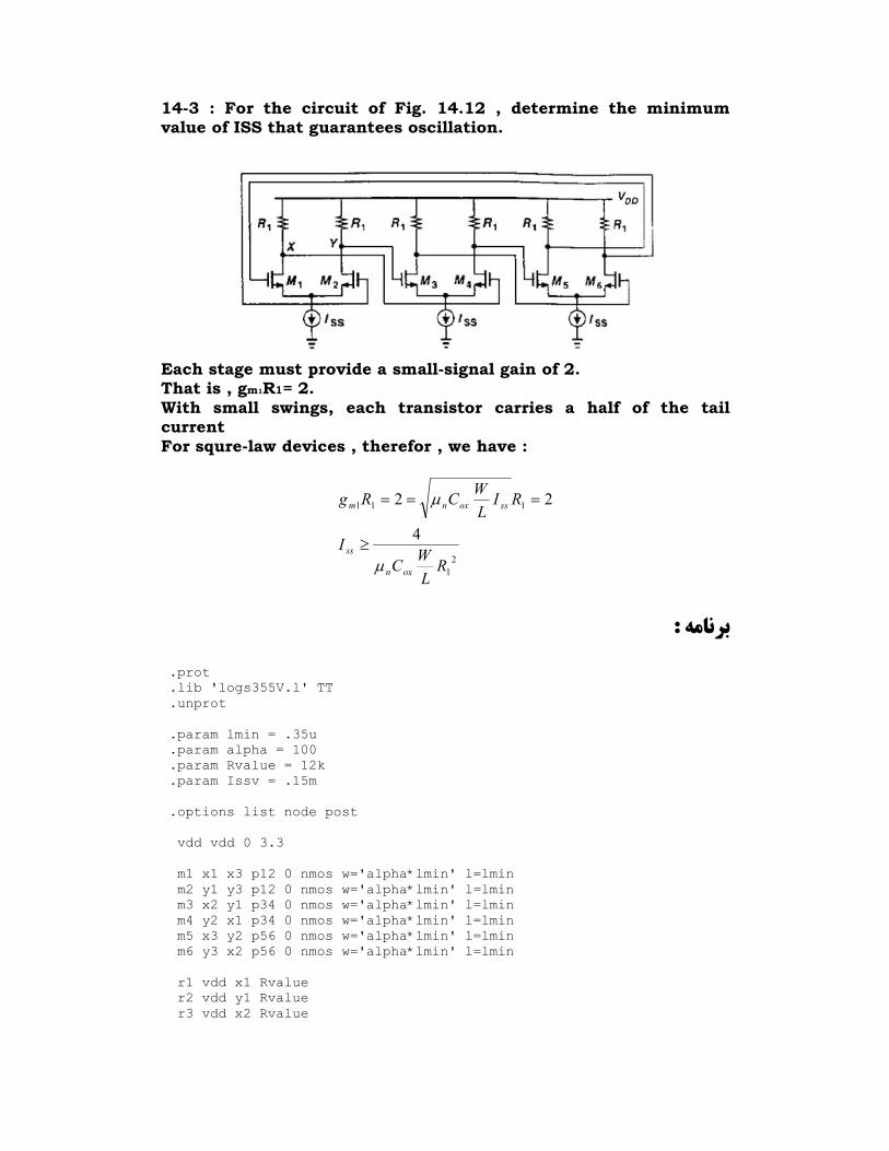
14-3 : For the circuit of Fig. 14.12 , determine the minimum value of ISS that guarantees oscillation.
Each stage must provide a small-signal gain of 2. That is , gm1R1= 2. With small swings, each transistor carries a half of the tail current For squre-law devices , therefor , we have :
2
1
111
4
22
RL
WC
I
RIL
WCRg
oxn
ss
ssoxnm
µ
µ
≥
===
:برنامه .prot
.lib 'logs355V.l' TT
.unprot
.param lmin = .35u
.param alpha = 100
.param Rvalue = 12k
.param Issv = .15m
.options list node post
vdd vdd 0 3.3
m1 x1 x3 p12 0 nmos w='alpha*lmin' l=lmin
m2 y1 y3 p12 0 nmos w='alpha*lmin' l=lmin
m3 x2 y1 p34 0 nmos w='alpha*lmin' l=lmin
m4 y2 x1 p34 0 nmos w='alpha*lmin' l=lmin
m5 x3 y2 p56 0 nmos w='alpha*lmin' l=lmin
m6 y3 x2 p56 0 nmos w='alpha*lmin' l=lmin
r1 vdd x1 Rvalue
r2 vdd y1 Rvalue
r3 vdd x2 Rvalue
:ادامه برنامه r4 vdd y2 Rvalue
r5 vdd x3 Rvalue
r6 vdd y3 Rvalue
Iss12 p12 0 Issv
Iss34 p34 0 Issv
Iss56 p56 0 Issv
.ic V(x1)=1;
.tran .001n 10n
.Probe ac V(x1)
.op
.end
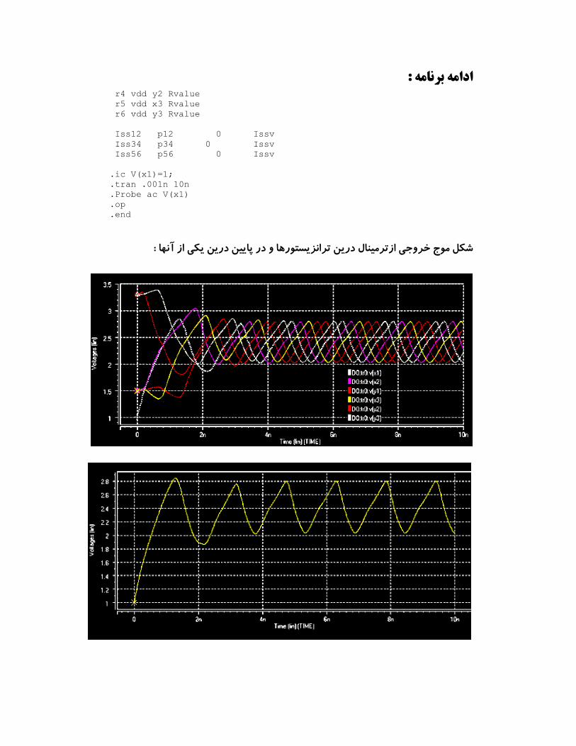
:ن درين يكي از آنها اييل درين ترانزيستورها و در پترميناشكل موج خروجي از

Fig. 14.8 : Set the value for each component in order to have an oscillation .
:برنامه
.prot
.lib 'logs355V.l' TT
.unprot
.param lmin = .35u
.param alpha = 120
.param RD = 680
.param CL = 120p
.options list node post
vdd vdd 0 3
m1 E G 0 0 nmos w='alpha*lmin'
+l=lmin
m2 F E 0 0 nmos w='alpha*lmin'
+l=lmin
m3 G F 0 0 nmos w='alpha*lmin'
+l=lmin
�
r1 vdd E RD
r2 vdd F RD
r3 vdd G RD
c1 E 0 CL
c2 F 0 CL
c3 G 0 CL
.ic V(E)=1;
.tran .01n 2u
.Probe V(G)
.op
.end