ACPL-217 DC Input, Half-Pitch Phototransistor Optocoupler ...
Upload
truongthuanCategory
view
214download
0
1
DESCRIPTIONDemonstration Circuit 1431A-D is a 2.3GHz to 4GHz high dynamic range downconverting mixer featuring the LTC®5543. The LTC5543 is part of a family of high dynamic range, passive downcon-verting mixers covering the 600MHz to 4GHz fre-quency range. The Demo Circuit 1431A-D and the LTC5543 are optimized for 2.3GHz to 4GHz RF applications. The LO frequency must fall within the 2.4GHz to 3.6GHz range for optimum performance.
The LTC5543 is designed for 3.3V operation, how-ever the IF amplifier can be powered by 5V for the highest P1dB. An integrated SPDT LO switch with fast switching accepts two active LO signals, while providing high isolation.
The LTC5543’s high conversion gain and high dy-namic range enable the use of lossy IF filters in high-selective receiver designs, while minimizing the total solution cost, board space and system-level variation.
High Dynamic Range Downconverting Mixer Family DEMO # IC PART # RF RANGE LO RANGE
DC1431A-A LTC5540 600MHz-1.3GHz 700MHz-1.2GHz DC1431A-B LTC5541 1.3GHz-2.3GHz 1.4GHz-2.0GHz DC1431A-C LTC5542 1.6GHz-2.7GHz 1.7GHz-2.5GHz DC1431A-D LTC5543 2.3GHz-4.0GHz 2.4GHz-3.6GHz
Design files for this circuit board are available. Call the LTC factory.
, LT, LTC, LTM, Linear Technology and the Linear Logo are registered trade-marks of Linear Technology Corporation. All other trademarks are the property of their respective owners.
TABLE 1. TYPICAL PERFORMANCE SUMMARY TA= 25°C, V CC = 3.3V, VCCIF = 3.3V, SHDN = Low, PLO = 0dBm, PRF = -3dBm (∆f = 2MHz for two-tone IIP3 tests), unless otherwise noted.
PARAMETER CONDITIONS VALUE UNITS
VCC Supply Voltage Range 3.1 to 3.5 V
VCCIF Supply Voltage Range 3.1 to 5.3 V
Total Supply Current (VCC + VCCIF) 201 mA
Total Supply Current During Shutdown SHDN = High ≤ 500 µA
SHDN Input Low Voltage (IC On) < 0.3 V
SHDN Input High Voltage (IC Off) > 3 V
LOSEL Input Low Voltage (LO1 Selected) < 0.3 V
LOSEL Input High Voltage (LO2 Selected) > 3 V
LO Input Frequency Range 2400 to 3600 MHz
LO Input Return Loss Z0 = 50Ω, fLO = 2400MHz to 3600MHz > 12 dB
LO Input Power Range fLO = 2400MHz to 3600MHz -4 to 6 dBm
RF Input Frequency Range Low-Side LO High-Side LO
2400 to 4000 2200 to 3200
MHz
RF Input Return Loss Z0 = 50Ω, fRF = 2200MHz to 3800MHz > 12 dB
DEMO CIRCUIT 1431A-DQUICK START GUIDE
LTC55432.3GHz to 4GHz
HIGH DYNAMIC RANGE DOWNCONVERTING MIXER
LTC5543
2
TYPICAL PERFORMANCE SUMMARY, CONTINUED TA= 25°C, V CC = 3.3V, VCCIF = 3.3V, SHDN = Low, PLO = 0dBm, PRF = -3dBm (∆f = 2MHz for two-tone IIP3 tests), unless otherwise noted.
IF Output Frequency (Can be re-matched for other frequencies.)
190 MHz
IF Output Return Loss > 12 dB
LO to RF Leakage fLO = 2400MHz to 3600MHz < -28 dBm
LO to IF Leakage fLO = 2400MHz to 3600MHz < -35 dBm
LO Switch Isolation LO1 Selected, 2400MHz < fLO < 3600MHz
LO2 Selected, 2400MHz < fLO < 3600MHz > 44 > 47
dB
RF to LO Isolation fRF = 2200MHz to 4000MHz > 37 dB
RF to IF Isolation fRF = 2200MHz to 4000MHz > 33 dB
Low-Side LO Downmixer Application: RF = 2400MHz to 3800MHz, IF = 190MHz, fLO = fRF – fIF
PARAMETER CONDITIONS VALUE UNITS
Conversion Gain RF = 2600MHz RF = 3300MHz RF = 3500MHz
8.9 7.1 6.7
dB
Input 3rd Order Intercept RF = 2600MHz RF = 3300MHz RF = 3500MHz
24.7 25.6 25.1
dBm
SSB Noise Figure RF = 2600MHz RF = 3300MHz RF = 3500MHz
9.6 11.6 11.8
dB
2RF – 2LO Output Spurious Product (fRF = fLO + fIF/2)
fRF = 3405MHz at -10dBm, fLO = 3310MHz -50 dBc
3RF – 3LO Output Spurious Product (fRF = fLO + fIF/3)
fRF = 3373.33MHz at -10dBm, fLO = 3310MHz -77 dBc
Input 1dB Compression RF = 3500MHz, VCCIF = 3.3V
RF = 3500MHz, VCCIF = 5V 11.3 11.8
dBm
High-Side LO Downmixer Application: RF = 2300MHz to 2700MHz, IF = 190MHz, fLO = fRF + fIF
PARAMETER CONDITIONS VALUE UNITS
Conversion Gain RF = 2300MHz RF = 2500MHz RF = 2700MHz
8.9 8.4 8.2
dB
Input 3rd Order Intercept RF = 2300MHz RF = 2500MHz RF = 2700MHz
23.8 24.5 24.4
dBm
SSB Noise Figure RF = 2300MHz RF = 2500MHz RF = 2700MHz
9.9 10.2 10.4
dB
SSB Noise Figure Under Blocking fRF = 2500MHz, fLO = 2690MHz
fBLOCK = 2300MHz, PBLOCK = 5dBm 17.5 dB
2LO – 2RF Output Spurious Product (fRF = fLO – fIF/2)
fRF = 2595MHz at -10dBm, fLO = 2690MHz -61 dBc
3LO – 3RF Output Spurious Product (fRF = fLO – fIF/3)
fRF = 2626.67MHz at -10dBm, fLO = 2690MHz -74 dBc
Input 1dB Compression RF = 2500MHz, VCCIF = 3.3V
RF = 2500MHz, VCCIF = 5V 10.9 13.9
dBm
LTC5543
3
APPLICATIONS NOTE For detailed applications information, please refer to the LTC5543 datasheet.
ABSOLUTE MAXIMUM RATINGS NOTE. Stresses beyond Absolute Maximum Ratings may cause permanent damage to the device. Exposure to any Absolute Maximum Rating condition for extended periods may affect device reliability and lifetime.
Mixer Supply Voltage (VCC1, VCC2)...........................3.8V LO Switch Supply Voltage (VCC3)..............................3.8V IF Supply Voltage (IF+, IF-) ........................................5.5V Shutdown Voltage (SHDN)................ -0.3V to VCC + 0.3V LO Select Voltage (LOSEL) .............. -0.3V to VCC + 0.3V LO1, LO2 Input Power (2GHz to 4GHz)...................9dBm LO1, LO2 Input DC Voltage .....................................±0.5V RF Input Power (2GHz to 4GHz) ...........................15dBm RF Input DC Voltage............................................... ±0.1V Operating Temperature Range.................... -40°C to 85°C
SUPPLY VOLTAGE RAMPING
Fast ramping of the supply voltage can cause a current glitch in the internal ESD protection circuits. Depending on the supply inductance, this could result in a supply voltage transient that exceeds the maximum rating. A supply voltage ramp time of greater than 1ms is recommended.
Do not clip powered test leads directly onto the demonstration circuit’s VCC and VCC_IF tur-rets. Instead, make all necessary connections with power supplies turned off, and then increase to op-erating voltage.
SHUTDOWN FEATURE
When the SHDN voltage is logic Low (<0.3V), the chip is enabled. When the SHDN voltage is logic High (>3V), the chip is disabled, and the current consumption is reduced to below 500µA. The SHDN must be pulled Low or High. If left floating, the On/Off state of the IC will be indeterminate. A logic table for the SHDN is shown in Table 2.
TABLE 2. SHDN LOGIC TABLE SHDN IC STATE Low On High Off
LO SWITCH
The LTC5543 features an integrated SPDT switch designed for high isolation and fast (<50ns) switching. The LO switch is controlled by the LOSEL logic control. The LOSEL must be pulled Low or High. If left floating, the LO selection will be indeterminate. A logic table for the LO switch is shown in Table 3.
TABLE 3. LO SWITCH LOGIC TABLE LOSEL ACTIVE LO INPUT
Low LO1 High LO2
RF INPUT
The RF input of Demonstration Circuit 1431A-D is matched to 50Ω from 2.2GHz to 4GHz with better than 12dB return loss. For the RF input to be matched, the selected LO input must be driven . The RF input impedance is somewhat dependent on LO frequency and, to a lesser ex-tend, LO input power.
LO INPUTS
The LTC5543’s LO amplifiers are optimized for the 2.4GHz to 3.6GHz LO frequency range. LO frequencies above and below this frequency range may be used with degraded performance.
The LO1 and LO2 inputs are always 50Ω-matched when VCC is applied to the chip, even when the chip is shutdown. The DC resistance of the selected LO input is approximately 20Ω, and the unselected input is approximately 50Ω.
The nominal LO input level is 0dBm. The LO input power range is between -4dBm and 6dBm. LO input power greater than 6dBm may cause conduction of the internal ESD diodes and should be avoided.
LTC5543
4
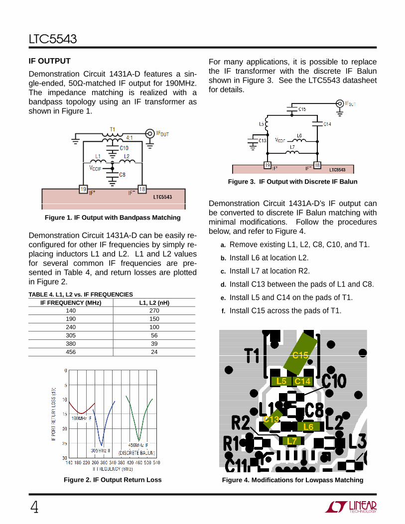
IF OUTPUT
Demonstration Circuit 1431A-D features a sin-gle-ended, 50Ω-matched IF output for 190MHz. The impedance matching is realized with a bandpass topology using an IF transformer as shown in Figure 1.
Figure 1. IF Output with Bandpass Matching Demonstration Circuit 1431A-D can be easily re-configured for other IF frequencies by simply re-placing inductors L1 and L2. L1 and L2 values for several common IF frequencies are pre-sented in Table 4, and return losses are plotted in Figure 2.
TABLE 4. L1, L2 vs. IF FREQUENCIES IF FREQUENCY (MHz) L1, L2 (nH)
140 270 190 150 240 100 305 56 380 39 456 24
Figure 2. IF Output Return Loss
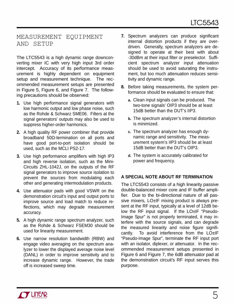
For many applications, it is possible to replace the IF transformer with the discrete IF Balun shown in Figure 3. See the LTC5543 datasheet for details.
Figure 3. IF Output with Discrete IF Balun
Demonstration Circuit 1431A-D’s IF output can be converted to discrete IF Balun matching with minimal modifications. Follow the procedures below, and refer to Figure 4.
a. Remove existing L1, L2, C8, C10, and T1.
b. Install L6 at location L2.
c. Install L7 at location R2.
d. Install C13 between the pads of L1 and C8.
e. Install L5 and C14 on the pads of T1.
f. Install C15 across the pads of T1.
Figure 4. Modifications for Lowpass Matching
LTC5543
5
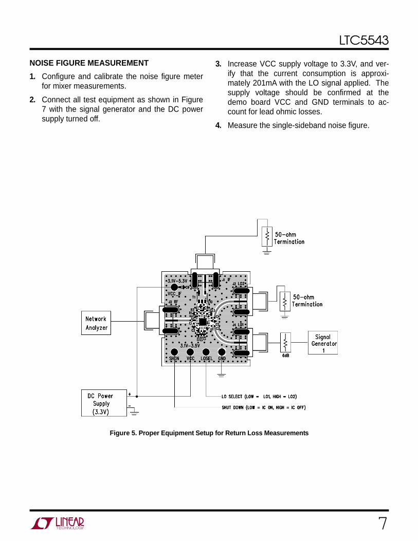
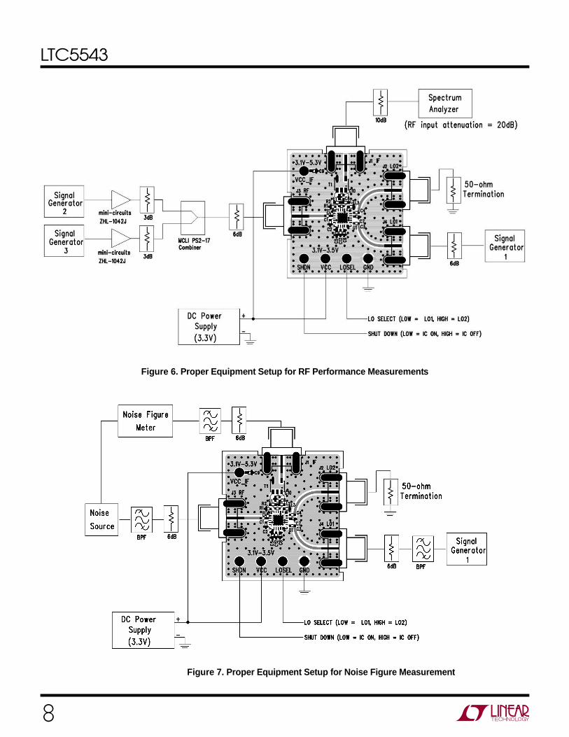
MEASUREMENT EQUIPMENT AND SETUP The LTC5543 is a high dynamic range downcon-verting mixer IC with very high input 3rd order intercept. Accuracy of its performance meas-urement is highly dependent on equipment setup and measurement technique. The rec-ommended measurement setups are presented in Figure 5, Figure 6, and Figure 7. The follow-ing precautions should be observed:
1. Use high performance signal generators with low harmonic output and low phase noise, such as the Rohde & Schwarz SME06. Filters at the signal generators’ outputs may also be used to suppress higher-order harmonics.
2. A high quality RF power combiner that provide broadband 50Ω-termination on all ports and have good port-to-port isolation should be used, such as the MCLI PS2-17.
3. Use high performance amplifiers with high IP3 and high reverse isolation, such as the Mini-Circuits ZHL-1042J, on the outputs of the RF signal generators to improve source isolation to prevent the sources from modulating each other and generating intermodulation products.
4. Use attenuator pads with good VSWR on the demonstration circuit’s input and output ports to improve source and load match to reduce re-flections, which may degrade measurement accuracy.
5. A high dynamic range spectrum analyzer, such as the Rohde & Schwarz FSEM30 should be used for linearity measurement.
6. Use narrow resolution bandwidth (RBW) and engage video averaging on the spectrum ana-lyzer to lower the displayed average noise level (DANL) in order to improve sensitivity and to increase dynamic range. However, the trade off is increased sweep time.
7. Spectrum analyzers can produce significant internal distortion products if they are over-driven. Generally, spectrum analyzers are de-signed to operate at their best with about -30dBm at their input filter or preselector. Suffi-cient spectrum analyzer input attenuation should be used to avoid saturating the instru-ment, but too much attenuation reduces sensi-tivity and dynamic range.
8. Before taking measurements, the system per-formance should be evaluated to ensure that:
a. Clean input signals can be produced. The two-tone signals’ OIP3 should be at least 15dB better than the DUT’s IIP3.
b. The spectrum analyzer’s internal distortion is minimized.
c. The spectrum analyzer has enough dy-namic range and sensitivity. The meas-urement system’s IIP3 should be at least 15dB better than the DUT’s OIP3.
d. The system is accurately calibrated for power and frequency.
A SPECIAL NOTE ABOUT RF TERMINATION
The LTC5543 consists of a high linearity passive double-balanced mixer core and IF buffer ampli-fier. Due to the bi-directional nature of all pas-sive mixers, LO±IF mixing product is always pre-sent at the RF input, typically at a level of 12dB be-low the RF input signal. If the LO±IF “Pseudo-Image Spur” is not properly terminated, it may in-terfere with the source signals, and can degrade the measured linearity and noise figure signifi-cantly. To avoid interference from the LO±IF “Pseudo-Image Spur”, terminate the RF input port with an isolator, diplexer, or attenuator. In the rec-ommended measurement setups presented in Figure 6 and Figure 7, the 6dB attenuator pad at the demonstration circuit’s RF input serves this purpose.
LTC5543
6
QUICK START PROCEDURE Demonstration circuit 1431A-D is easy to set up to evaluate the performance of the LTC5543. Refer to Figure 5, Figure 6, and Figure 7 for proper equipment connections and follow the procedure below:
NOTE. Care should be taken to never exceed absolute maximum input ratings. Make all connections with RF and DC power off.
RETURN LOSS MEASUREMENTS
1. Configure the Network Analyzer for return loss measurement, set appropriate frequency range, and set the test signal to -3dBm.
2. Calibrate the Network Analyzer.
3. Connect all test equipment as shown in Figure 5 with the signal generator and the DC power supply turned off.
4. Increase VCC supply voltage to 3.3V, and ver-ify that the current consumption is approxi-mately 201mA with the LO signal applied. The supply voltage should be confirmed at the demo board VCC and GND terminals to ac-count for lead ohmic losses.
5. With the LO signal applied, and the unused demo board ports terminated in 50Ω, measure return losses of the RF input and IF output ports.
6. Set the test signal to 0dBm, and re-calibrate the Network Analyzer.
7. Terminate the RF input, the IF output, and the unused LO port in 50Ω. Measure return losses of the LO input ports.
RF PERFORMANCE MEASUREMENTS
1. Connect all test equipment as shown in Figure 6 with the signal generators and the DC power supply turned off.
2. Increase VCC supply voltage to 3.3V, and ver-ify that the current consumption is approxi-mately 201mA with the LO signal applied. The supply voltage should be confirmed at the
demo board VCC and GND terminals to ac-count for lead ohmic losses.
3. Set the LO source (Signal Generator 1) to pro-vide a 0dBm, CW signal to the selected demo board LO input port at appropriate LO fre-quency.
4. Set the RF sources (Signal Generators 2 and 3) to provide two -3dBm CW signals, 2MHz apart, to the demo board RF input port at the appropriate RF frequency.
5. Measure the resulting IF output on the Spec-trum Analyzer:
a. The wanted two-tone IF output signals are at:
fIF1 = fRF1 - fLO, and fIF2 = fRF2 - fLO for low-side LO, and fIF1 = fLO - fRF1, and fIF2 = fLO - fRF2 for high-side LO
b. The 3rd order intermodulation products which are closest to the wanted IF signals are used to calculate the Input 3rd Order In-tercept:
fIM3,1 = fRF1 - fLO - ∆IF, and fIM3,2 = fRF2 - fLO + ∆IF for low-side LO, and fIM3,1 = fLO - fRF1 + ∆IF, and fIM3,2 = fLO - fRF2 - ∆IF for high-side LO Where ∆IF = fRF2 - fRF1.
6. Calculate Input 3rd Order Intercept:
IIP3 = (∆IM3)/2 + PRF
Where ∆IM3 = PIF - PIM3. PIF is the lowest IF output signal power at either fIF1 or fIF2. PIM3 is the highest 3rd order intermodulation product power at either fIM3,1 or fIM3,2. PRF is the per-tone RF input power.
7. Turn off one of the RF signal generators, and measure Conversion Gain, RF to IF isolation, LO to IF leakage, and Input 1dB compression point.
LTC5543
7
NOISE FIGURE MEASUREMENT
1. Configure and calibrate the noise figure meter for mixer measurements.
2. Connect all test equipment as shown in Figure 7 with the signal generator and the DC power supply turned off.
3. Increase VCC supply voltage to 3.3V, and ver-ify that the current consumption is approxi-mately 201mA with the LO signal applied. The supply voltage should be confirmed at the demo board VCC and GND terminals to ac-count for lead ohmic losses.
4. Measure the single-sideband noise figure.
Figure 5. Proper Equipment Setup for Return Loss Me asurements
LTC5543
8
Figure 6. Proper Equipment Setup for RF Performance Measurements
Figure 7. Proper Equipment Setup for Noise Figure M easurement
LTC5543
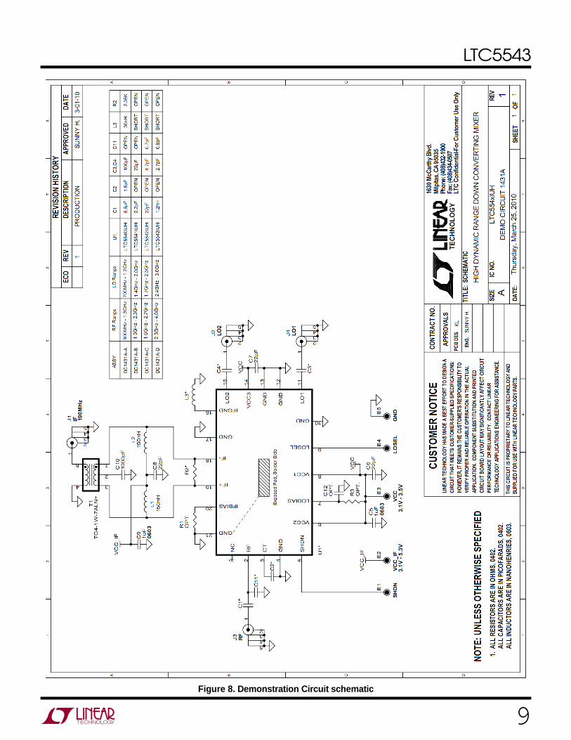
9Figure 8. Demonstration Circuit schematic