N-channel 600 V, 0.06 typ., 42 A MDmesh™ M2 Power MOSFET in ...
0
3
6
9
12
15
18
21
24
0 2 4 6 8 10 12 14 16 18 20VGS - Gate-to- Source Voltage (V)
RD
S(o
n) -
On-
Sta
te R
esis
tanc
e (
mΩ
) TC = 25°C, I D = 18ATC = 125°C, I D = 18A
G001
0
1
2
3
4
5
6
7
8
9
10
0 2 4 6 8 10 12 14 16Qg - Gate Charge (nC)
VG
S -
Gat
e-to
-Sou
rce
Vol
tage
(V
) ID = 18AVDS = 30V
G001
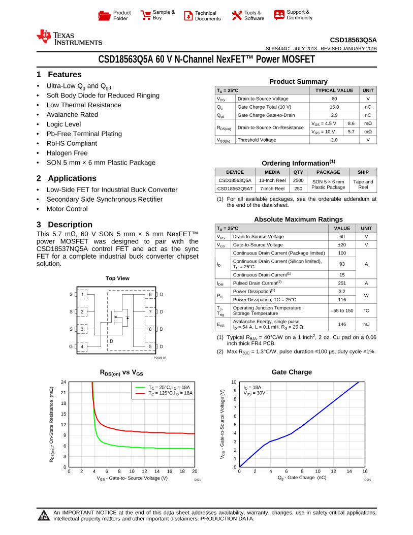
1 D
2 D
3 D
4
D
D5G
6S
7S
8S
P0093-01
Product
Folder
Sample &Buy
Technical
Documents
Tools &
Software
Support &Community
An IMPORTANT NOTICE at the end of this data sheet addresses availability, warranty, changes, use in safety-critical applications,intellectual property matters and other important disclaimers. PRODUCTION DATA.
CSD18563Q5ASLPS444C –JULY 2013–REVISED JANUARY 2016
CSD18563Q5A 60 V N-Channel NexFET™ Power MOSFET
1
1 Features1• Ultra-Low Qg and Qgd
• Soft Body Diode for Reduced Ringing• Low Thermal Resistance• Avalanche Rated• Logic Level• Pb-Free Terminal Plating• RoHS Compliant• Halogen Free• SON 5 mm × 6 mm Plastic Package
2 Applications• Low-Side FET for Industrial Buck Converter• Secondary Side Synchronous Rectifier• Motor Control
3 DescriptionThis 5.7 mΩ, 60 V SON 5 mm × 6 mm NexFET™power MOSFET was designed to pair with theCSD18537NQ5A control FET and act as the syncFET for a complete industrial buck converter chipsetsolution.
Top View
Product SummaryTA = 25°C TYPICAL VALUE UNIT
VDS Drain-to-Source Voltage 60 V
Qg Gate Charge Total (10 V) 15.0 nC
Qgd Gate Charge Gate-to-Drain 2.9 nC
RDS(on) Drain-to-Source On-ResistanceVGS = 4.5 V 8.6 mΩ
VGS = 10 V 5.7 mΩ
VGS(th) Threshold Voltage 2.0 V
.Ordering Information(1)
DEVICE MEDIA QTY PACKAGE SHIP
CSD18563Q5A 13-Inch Reel 2500 SON 5 × 6 mmPlastic Package
Tape andReelCSD18563Q5AT 7-Inch Reel 250
(1) For all available packages, see the orderable addendum atthe end of the data sheet.
Absolute Maximum RatingsTA = 25°C VALUE UNIT
VDS Drain-to-Source Voltage 60 V
VGS Gate-to-Source Voltage ±20 V
ID
Continuous Drain Current (Package limited) 100
AContinuous Drain Current (Silicon limited),TC = 25°C 93
Continuous Drain Current(1) 15
IDM Pulsed Drain Current(2) 251 A
PDPower Dissipation(1) 3.2
WPower Dissipation, TC = 25°C 116
TJ,Tstg
Operating Junction Temperature,Storage Temperature –55 to 150 °C
EASAvalanche Energy, single pulseID = 54 A, L = 0.1 mH, RG = 25 Ω 146 mJ
(1) Typical RθJA = 40°C/W on a 1 inch2, 2 oz. Cu pad on a 0.06inch thick FR4 PCB.
(2) Max RθJC = 1.3°C/W, pulse duration ≤100 μs, duty cycle ≤1%.
RDS(on) vs VGS Gate Charge
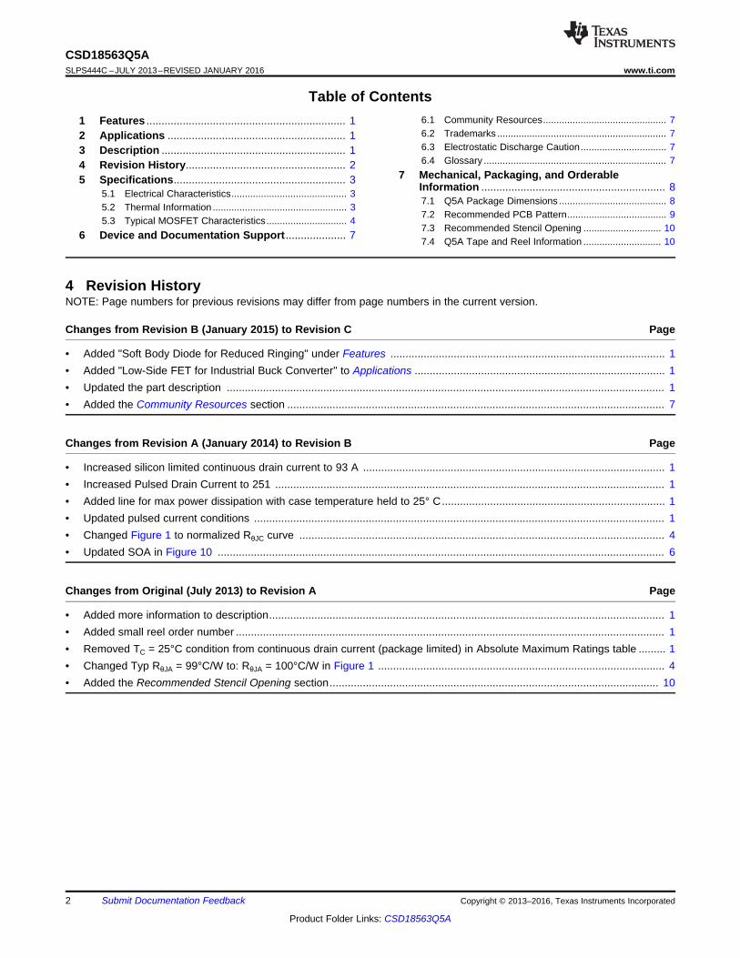
2
CSD18563Q5ASLPS444C –JULY 2013–REVISED JANUARY 2016 www.ti.com
Product Folder Links: CSD18563Q5A
Submit Documentation Feedback Copyright © 2013–2016, Texas Instruments Incorporated
Table of Contents1 Features .................................................................. 12 Applications ........................................................... 13 Description ............................................................. 14 Revision History..................................................... 25 Specifications......................................................... 3
5.1 Electrical Characteristics........................................... 35.2 Thermal Information .................................................. 35.3 Typical MOSFET Characteristics.............................. 4
6 Device and Documentation Support.................... 7
6.1 Community Resources.............................................. 76.2 Trademarks ............................................................... 76.3 Electrostatic Discharge Caution................................ 76.4 Glossary .................................................................... 7
7 Mechanical, Packaging, and OrderableInformation ............................................................. 87.1 Q5A Package Dimensions ........................................ 87.2 Recommended PCB Pattern..................................... 97.3 Recommended Stencil Opening ............................. 107.4 Q5A Tape and Reel Information ............................. 10
4 Revision HistoryNOTE: Page numbers for previous revisions may differ from page numbers in the current version.
Changes from Revision B (January 2015) to Revision C Page
• Added "Soft Body Diode for Reduced Ringing" under Features ........................................................................................... 1• Added "Low-Side FET for Industrial Buck Converter" to Applications ................................................................................... 1• Updated the part description ................................................................................................................................................. 1• Added the Community Resources section ............................................................................................................................. 7
Changes from Revision A (January 2014) to Revision B Page
• Increased silicon limited continuous drain current to 93 A .................................................................................................... 1• Increased Pulsed Drain Current to 251 ................................................................................................................................. 1• Added line for max power dissipation with case temperature held to 25° C.......................................................................... 1• Updated pulsed current conditions ........................................................................................................................................ 1• Changed Figure 1 to normalized RθJC curve ......................................................................................................................... 4• Updated SOA in Figure 10 .................................................................................................................................................... 6
Changes from Original (July 2013) to Revision A Page
• Added more information to description................................................................................................................................... 1• Added small reel order number .............................................................................................................................................. 1• Removed TC = 25°C condition from continuous drain current (package limited) in Absolute Maximum Ratings table ......... 1• Changed Typ RθJA = 99°C/W to: RθJA = 100°C/W in Figure 1 ............................................................................................... 4• Added the Recommended Stencil Opening section............................................................................................................. 10
3
CSD18563Q5Awww.ti.com SLPS444C –JULY 2013–REVISED JANUARY 2016
Product Folder Links: CSD18563Q5A
Submit Documentation FeedbackCopyright © 2013–2016, Texas Instruments Incorporated
5 Specifications
5.1 Electrical Characteristics(TA = 25°C unless otherwise stated)
PARAMETER TEST CONDITIONS MIN TYP MAX UNITSTATIC CHARACTERISTICSBVDSS Drain-to-source voltage VGS = 0 V, ID = 250 μA 60 VIDSS Drain-to-source leakage current VGS = 0 V, VDS = 48 V 1 μAIGSS Gate-to-source leakage current VDS = 0 V, VGS = 20 V 100 nAVGS(th) Gate-to-source threshold voltage VDS = VGS, ID = 250 μA 1.7 2.0 2.4 V
RDS(on) Drain-to-source on resistanceVGS = 4.5 V, ID = 18 A 8.6 10.8 mΩVGS = 10 V, ID = 18 A 5.7 6.8 mΩ
gfs Transconductance VDS = 30 V, ID = 18 A 60 SDYNAMIC CHARACTERISTICSCiss Input capacitance
VGS = 0 V, VDS = 30 V, ƒ = 1 MHz1150 1500 pF
Coss Output capacitance 280 364 pFCrss Reverse transfer capacitance 3.9 5.1 pFRG Series gate resistance 1.5 3.0 ΩQg Gate charge total (4.5 V)
VDS = 30 V, ID = 18 A
7.3 9.5nC
Qg Gate charge total (10 V) 15 20Qgd Gate charge gate-to-drain 2.9 nCQgs Gate charge gate-to-source 3.3 nCQg(th) Gate charge at Vth 2.3 nCQoss Output charge VDS = 30 V, VGS = 0 V 36 nCtd(on) Turn on delay time
VDS = 30 V, VGS = 10 V, IDS = 18 A, RG = 0 Ω
3.2 nstr Rise time 6.3 nstd(off) Turn off delay time 11.4 nstf Fall time 1.7 nsDIODE CHARACTERISTICSVSD Diode forward voltage ISD = 18 A, VGS = 0 V 0.8 1 VQrr Reverse recovery charge
VDS= 30 V, IF = 18 A, di/dt = 300 A/μs63 nC
trr Reverse recovery time 49 ns
(1) RθJC is determined with the device mounted on a 1 inch2 (6.45 cm2), 2 oz. (0.071 mm thick) Cu pad on a 1.5 inch × 1.5 inch (3.81 cm ×3.81 cm), 0.06 inch (1.52 mm) thick FR4 PCB. RθJC is specified by design, whereas RθJA is determined by the user’s board design.
(2) Device mounted on FR4 material with 1 inch2 (6.45 cm2), 2 oz. (0.071 mm thick) Cu.
5.2 Thermal Information(TA = 25°C unless otherwise stated)
THERMAL METRIC MIN TYP MAX UNITRθJC Junction-to-case thermal resistance (1) 1.3
°C/WRθJA Junction-to-ambient thermal resistance (1) (2) 50
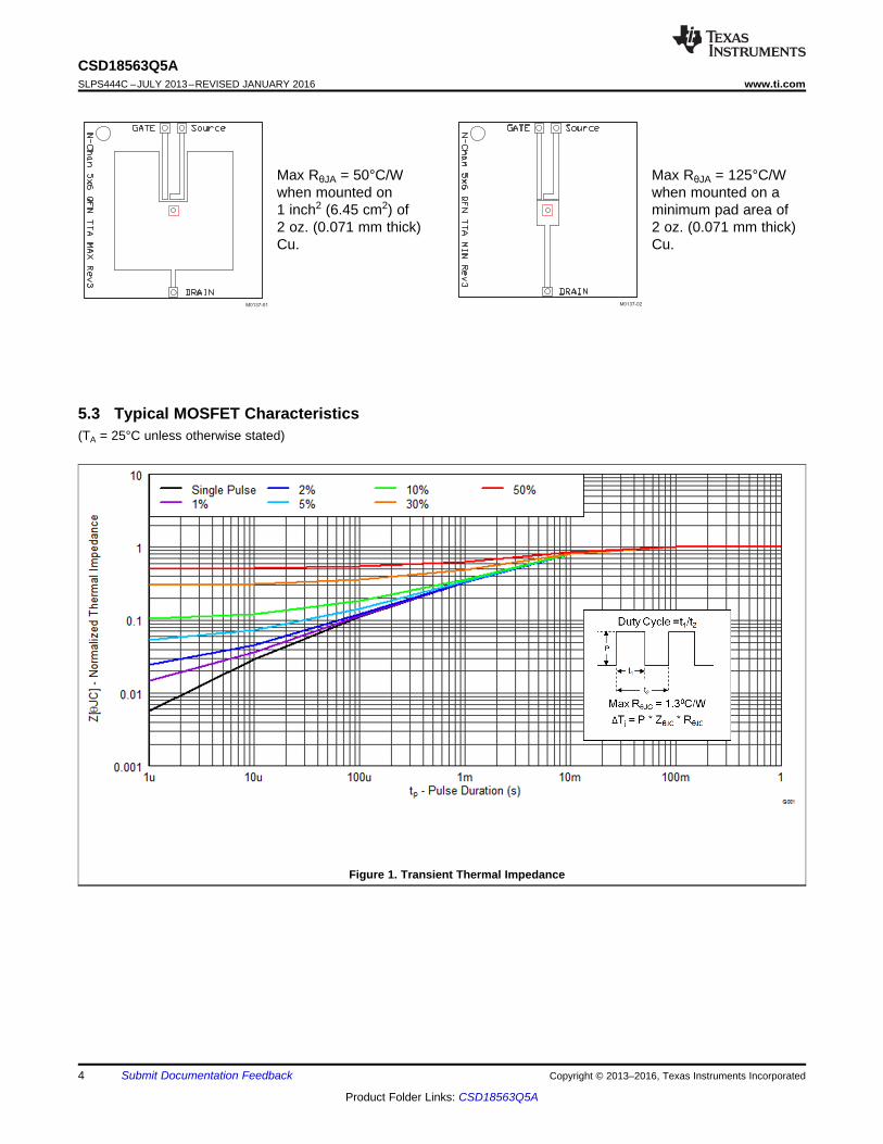
GATE Source
DRAIN
N-Chan 5x6 QFN TTA MAX Rev3
M0137-01
GATE Source
DRAIN
N-Chan 5x6 QFN TTA MIN Rev3
M0137-02
4
CSD18563Q5ASLPS444C –JULY 2013–REVISED JANUARY 2016 www.ti.com
Product Folder Links: CSD18563Q5A
Submit Documentation Feedback Copyright © 2013–2016, Texas Instruments Incorporated
Max RθJA = 50°C/Wwhen mounted on1 inch2 (6.45 cm2) of2 oz. (0.071 mm thick)Cu.
Max RθJA = 125°C/Wwhen mounted on aminimum pad area of2 oz. (0.071 mm thick)Cu.
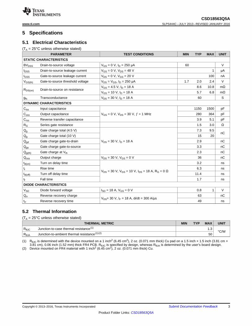
5.3 Typical MOSFET Characteristics(TA = 25°C unless otherwise stated)
Figure 1. Transient Thermal Impedance
1
1.2
1.4
1.6
1.8
2
2.2
2.4
2.6
−75 −25 25 75 125 175TC - Case Temperature (ºC)
VG
S(th
) - T
hres
hold
Vol
tage
(V
)
ID = 250uA
G001
0
3
6
9
12
15
18
21
24
0 2 4 6 8 10 12 14 16 18 20VGS - Gate-to- Source Voltage (V)
RD
S(o
n) -
On-
Sta
te R
esis
tanc
e (
mΩ
) TC = 25°C, I D = 18ATC = 125°C, I D = 18A
G001
0
1
2
3
4
5
6
7
8
9
10
0 2 4 6 8 10 12 14 16Qg - Gate Charge (nC)
VG
S -
Gat
e-to
-Sou
rce
Vol
tage
(V
) ID = 18AVDS = 30V
G001
1
10
100
1000
1000020000
0 10 20 30 40 50 60VDS - Drain-to-Source Voltage (V)
C −
Cap
acita
nce
(pF
)Ciss = Cgd + CgsCoss = Cds + CgdCrss = Cgd
G001
0
20
40
60
80
100
120
140
160
180
200
0 1 2 3 4 5VDS - Drain-to-Source Voltage (V)
I DS -
Dra
in-t
o-S
ourc
e C
urre
nt (
A)
VGS =10VVGS =6VVGS =4.5V
G001
0
10
20
30
40
50
60
70
80
90
100
0 1 2 3 4 5 6VGS - Gate-to-Source Voltage (V)
I DS -
Dra
in-t
o-S
ourc
e C
urre
nt (
A)
TC = 125°CTC = 25°CTC = −55°C
VDS = 5V
G001
5
CSD18563Q5Awww.ti.com SLPS444C –JULY 2013–REVISED JANUARY 2016
Product Folder Links: CSD18563Q5A
Submit Documentation FeedbackCopyright © 2013–2016, Texas Instruments Incorporated
Typical MOSFET Characteristics (continued)(TA = 25°C unless otherwise stated)
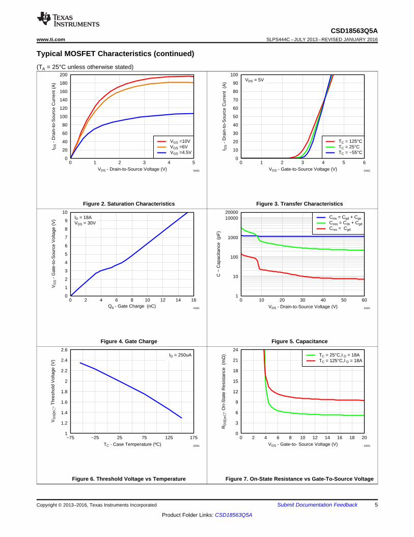
Figure 2. Saturation Characteristics Figure 3. Transfer Characteristics
Figure 4. Gate Charge Figure 5. Capacitance
Figure 6. Threshold Voltage vs Temperature Figure 7. On-State Resistance vs Gate-To-Source Voltage
0
20
40
60
80
100
120
−50 −25 0 25 50 75 100 125 150 175TC - Case Temperature (ºC)
I DS -
Dra
in-
to-
Sou
rce
Cur
rent
(A
)
G001
0.1
1
10
100
1000
5000
0.1 1 10 100VDS - Drain-to-Source Voltage (V)
I DS -
Dra
in-t
o-S
ourc
e C
urre
nt (
A) 10us
100us1ms10ms
DC
Single PulseMax RthetaJC = 1.3ºC/W
G001
10
100
0.01 0.1 1TAV - Time in Avalanche (mS)
I AV -
Pea
k A
vala
nche
Cur
rent
(A
) TC = 25ºCTC = 125ºC
G001
0.3
0.6
0.9
1.2
1.5
1.8
2.1
2.4
−75 −25 25 75 125 175TC - Case Temperature (ºC)
Nor
mal
ized
On-
Sta
te R
esis
tanc
e
VGS = 4.5VVGS = 10V
ID =18A
G001
0.0001
0.001
0.01
0.1
1
10
100
0 0.2 0.4 0.6 0.8 1VSD − Source-to-Drain Voltage (V)
I SD −
Sou
rce-
to-D
rain
Cur
rent
(A
) TC = 25°CTC = 125°C
G001
6
CSD18563Q5ASLPS444C –JULY 2013–REVISED JANUARY 2016 www.ti.com
Product Folder Links: CSD18563Q5A
Submit Documentation Feedback Copyright © 2013–2016, Texas Instruments Incorporated
Typical MOSFET Characteristics (continued)(TA = 25°C unless otherwise stated)
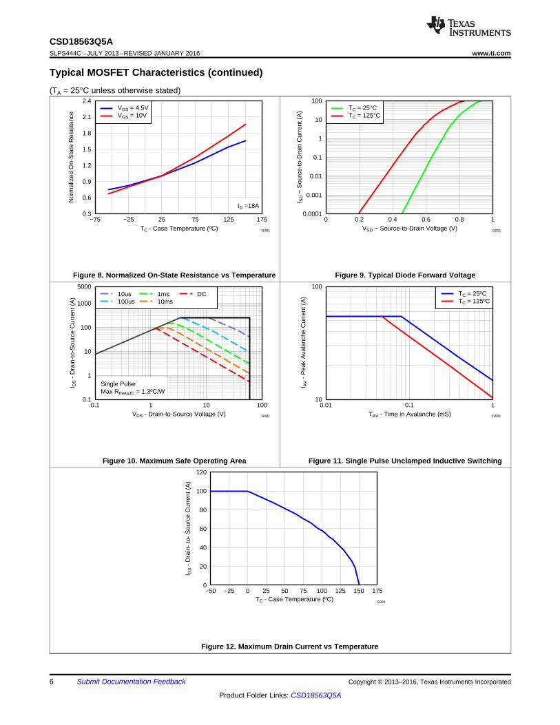
Figure 8. Normalized On-State Resistance vs Temperature Figure 9. Typical Diode Forward Voltage
Figure 10. Maximum Safe Operating Area Figure 11. Single Pulse Unclamped Inductive Switching
Figure 12. Maximum Drain Current vs Temperature
7
CSD18563Q5Awww.ti.com SLPS444C –JULY 2013–REVISED JANUARY 2016
Product Folder Links: CSD18563Q5A
Submit Documentation FeedbackCopyright © 2013–2016, Texas Instruments Incorporated
6 Device and Documentation Support
6.1 Community ResourcesThe following links connect to TI community resources. Linked contents are provided "AS IS" by the respectivecontributors. They do not constitute TI specifications and do not necessarily reflect TI's views; see TI's Terms ofUse.
TI E2E™ Online Community TI's Engineer-to-Engineer (E2E) Community. Created to foster collaborationamong engineers. At e2e.ti.com, you can ask questions, share knowledge, explore ideas and helpsolve problems with fellow engineers.
Design Support TI's Design Support Quickly find helpful E2E forums along with design support tools andcontact information for technical support.
6.2 TrademarksNexFET, E2E are trademarks of Texas Instruments.All other trademarks are the property of their respective owners.
6.3 Electrostatic Discharge CautionThese devices have limited built-in ESD protection. The leads should be shorted together or the device placed in conductive foamduring storage or handling to prevent electrostatic damage to the MOS gates.
6.4 GlossarySLYZ022 — TI Glossary.
This glossary lists and explains terms, acronyms, and definitions.
12
556
781
42
3
34
67
8
8
CSD18563Q5ASLPS444C –JULY 2013–REVISED JANUARY 2016 www.ti.com
Product Folder Links: CSD18563Q5A
Submit Documentation Feedback Copyright © 2013–2016, Texas Instruments Incorporated
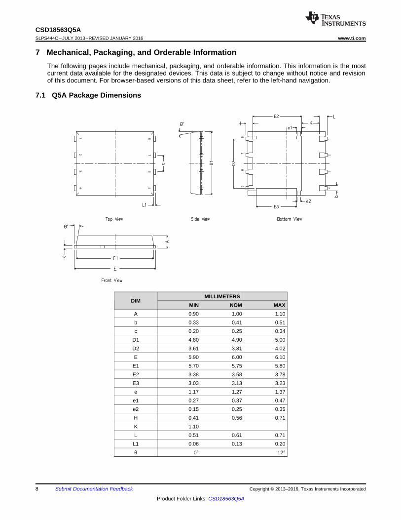
7 Mechanical, Packaging, and Orderable InformationThe following pages include mechanical, packaging, and orderable information. This information is the mostcurrent data available for the designated devices. This data is subject to change without notice and revisionof this document. For browser-based versions of this data sheet, refer to the left-hand navigation.
7.1 Q5A Package Dimensions
DIMMILLIMETERS
MIN NOM MAXA 0.90 1.00 1.10b 0.33 0.41 0.51c 0.20 0.25 0.34
D1 4.80 4.90 5.00D2 3.61 3.81 4.02E 5.90 6.00 6.10E1 5.70 5.75 5.80E2 3.38 3.58 3.78E3 3.03 3.13 3.23e 1.17 1.27 1.37e1 0.27 0.37 0.47e2 0.15 0.25 0.35H 0.41 0.56 0.71K 1.10L 0.51 0.61 0.71L1 0.06 0.13 0.20θ 0° 12°
F10
F11
F6 F7
F5
F9
F4
F8
145
8
M0139-01
F2
F3
F1
9
CSD18563Q5Awww.ti.com SLPS444C –JULY 2013–REVISED JANUARY 2016
Product Folder Links: CSD18563Q5A
Submit Documentation FeedbackCopyright © 2013–2016, Texas Instruments Incorporated
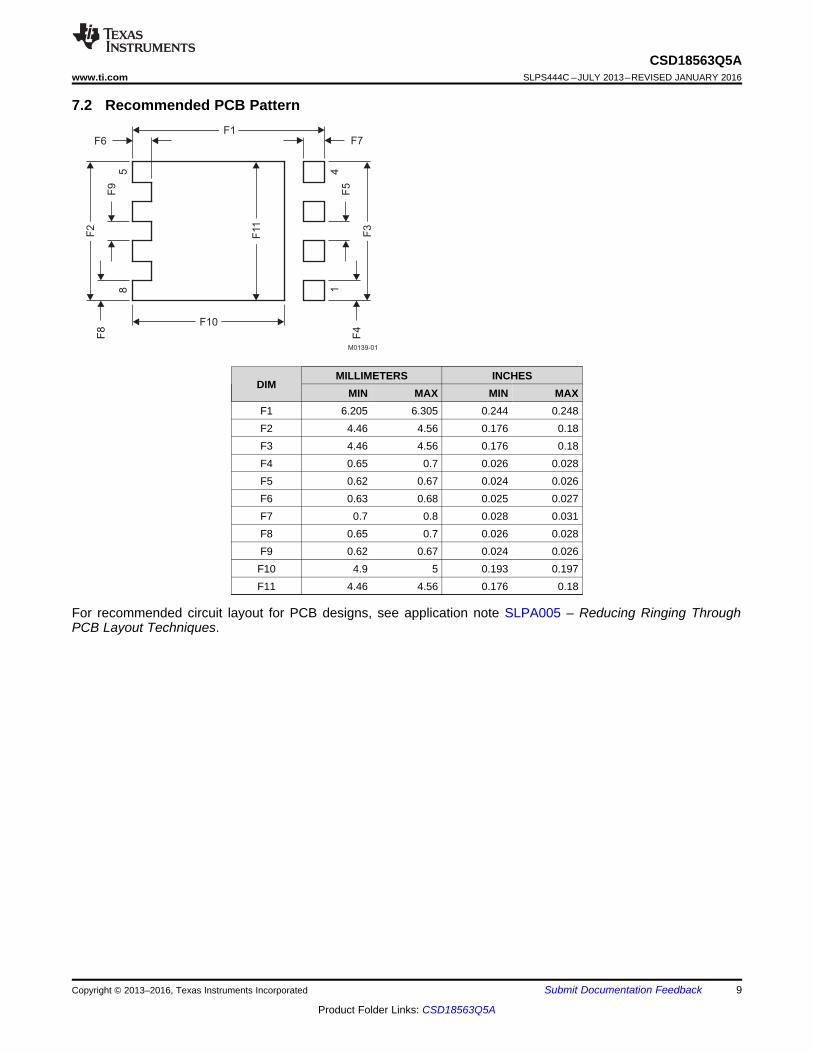
7.2 Recommended PCB Pattern
DIMMILLIMETERS INCHES
MIN MAX MIN MAXF1 6.205 6.305 0.244 0.248F2 4.46 4.56 0.176 0.18F3 4.46 4.56 0.176 0.18F4 0.65 0.7 0.026 0.028F5 0.62 0.67 0.024 0.026F6 0.63 0.68 0.025 0.027F7 0.7 0.8 0.028 0.031F8 0.65 0.7 0.026 0.028F9 0.62 0.67 0.024 0.026F10 4.9 5 0.193 0.197F11 4.46 4.56 0.176 0.18
For recommended circuit layout for PCB designs, see application note SLPA005 – Reducing Ringing ThroughPCB Layout Techniques.
Ø 1.50+0.10–0.00
4.00 ±0.10 (See Note 1)
1.7
5 ±
0.1
0
R 0.30 TYP
Ø 1.50 MIN
A0
K0
0.30 ±0.05
R 0.30 MAX
A0 = 6.50 ±0.10B0 = 5.30 ±0.10K0 = 1.40 ±0.10
M0138-01
2.00 ±0.05
8.00 ±0.10
B012.0
0 ±
0.3
0
5.5
0 ±
0.0
5
4.310
58 1
4
3.020
0.500
1.5701.270
0.615 1.105
0.500
1.585 1.235
0.620
0.500
(0.020) 8x
(0.020)
(0.020) 8x
(0.024)
(0.062)
4x (0.050)
(0.044)(0.024)
(0.119)
(0.062) (0.049)
(0.170)
0.385(0.015)
10
CSD18563Q5ASLPS444C –JULY 2013–REVISED JANUARY 2016 www.ti.com
Product Folder Links: CSD18563Q5A
Submit Documentation Feedback Copyright © 2013–2016, Texas Instruments Incorporated
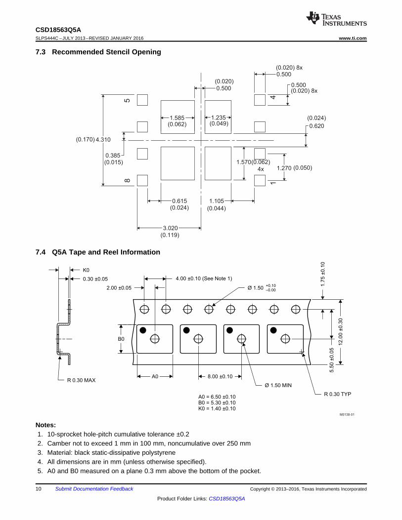
7.3 Recommended Stencil Opening
7.4 Q5A Tape and Reel Information
Notes:1. 10-sprocket hole-pitch cumulative tolerance ±0.22. Camber not to exceed 1 mm in 100 mm, noncumulative over 250 mm3. Material: black static-dissipative polystyrene4. All dimensions are in mm (unless otherwise specified).5. A0 and B0 measured on a plane 0.3 mm above the bottom of the pocket.
PACKAGE OPTION ADDENDUM
www.ti.com 25-Apr-2017
Addendum-Page 1
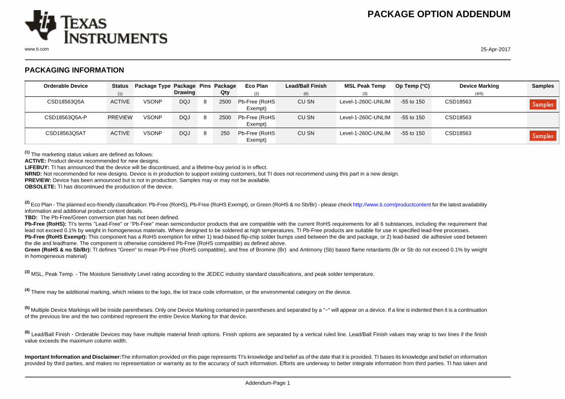
PACKAGING INFORMATION
Orderable Device Status(1)
Package Type PackageDrawing
Pins PackageQty
Eco Plan(2)
Lead/Ball Finish(6)
MSL Peak Temp(3)
Op Temp (°C) Device Marking(4/5)
Samples
CSD18563Q5A ACTIVE VSONP DQJ 8 2500 Pb-Free (RoHSExempt)
CU SN Level-1-260C-UNLIM -55 to 150 CSD18563
CSD18563Q5A-P PREVIEW VSONP DQJ 8 2500 Pb-Free (RoHSExempt)
CU SN Level-1-260C-UNLIM -55 to 150 CSD18563
CSD18563Q5AT ACTIVE VSONP DQJ 8 250 Pb-Free (RoHSExempt)
CU SN Level-1-260C-UNLIM -55 to 150 CSD18563
(1) The marketing status values are defined as follows:ACTIVE: Product device recommended for new designs.LIFEBUY: TI has announced that the device will be discontinued, and a lifetime-buy period is in effect.NRND: Not recommended for new designs. Device is in production to support existing customers, but TI does not recommend using this part in a new design.PREVIEW: Device has been announced but is not in production. Samples may or may not be available.OBSOLETE: TI has discontinued the production of the device.
(2) Eco Plan - The planned eco-friendly classification: Pb-Free (RoHS), Pb-Free (RoHS Exempt), or Green (RoHS & no Sb/Br) - please check http://www.ti.com/productcontent for the latest availabilityinformation and additional product content details.TBD: The Pb-Free/Green conversion plan has not been defined.Pb-Free (RoHS): TI's terms "Lead-Free" or "Pb-Free" mean semiconductor products that are compatible with the current RoHS requirements for all 6 substances, including the requirement thatlead not exceed 0.1% by weight in homogeneous materials. Where designed to be soldered at high temperatures, TI Pb-Free products are suitable for use in specified lead-free processes.Pb-Free (RoHS Exempt): This component has a RoHS exemption for either 1) lead-based flip-chip solder bumps used between the die and package, or 2) lead-based die adhesive used betweenthe die and leadframe. The component is otherwise considered Pb-Free (RoHS compatible) as defined above.Green (RoHS & no Sb/Br): TI defines "Green" to mean Pb-Free (RoHS compatible), and free of Bromine (Br) and Antimony (Sb) based flame retardants (Br or Sb do not exceed 0.1% by weightin homogeneous material)
(3) MSL, Peak Temp. - The Moisture Sensitivity Level rating according to the JEDEC industry standard classifications, and peak solder temperature.
(4) There may be additional marking, which relates to the logo, the lot trace code information, or the environmental category on the device.
(5) Multiple Device Markings will be inside parentheses. Only one Device Marking contained in parentheses and separated by a "~" will appear on a device. If a line is indented then it is a continuationof the previous line and the two combined represent the entire Device Marking for that device.
(6) Lead/Ball Finish - Orderable Devices may have multiple material finish options. Finish options are separated by a vertical ruled line. Lead/Ball Finish values may wrap to two lines if the finishvalue exceeds the maximum column width.
Important Information and Disclaimer:The information provided on this page represents TI's knowledge and belief as of the date that it is provided. TI bases its knowledge and belief on informationprovided by third parties, and makes no representation or warranty as to the accuracy of such information. Efforts are underway to better integrate information from third parties. TI has taken and
PACKAGE OPTION ADDENDUM
www.ti.com 25-Apr-2017
Addendum-Page 2
continues to take reasonable steps to provide representative and accurate information but may not have conducted destructive testing or chemical analysis on incoming materials and chemicals.TI and TI suppliers consider certain information to be proprietary, and thus CAS numbers and other limited information may not be available for release.
In no event shall TI's liability arising out of such information exceed the total purchase price of the TI part(s) at issue in this document sold by TI to Customer on an annual basis.
IMPORTANT NOTICE
Texas Instruments Incorporated (TI) reserves the right to make corrections, enhancements, improvements and other changes to itssemiconductor products and services per JESD46, latest issue, and to discontinue any product or service per JESD48, latest issue. Buyersshould obtain the latest relevant information before placing orders and should verify that such information is current and complete.TI’s published terms of sale for semiconductor products (http://www.ti.com/sc/docs/stdterms.htm) apply to the sale of packaged integratedcircuit products that TI has qualified and released to market. Additional terms may apply to the use or sale of other types of TI products andservices.Reproduction of significant portions of TI information in TI data sheets is permissible only if reproduction is without alteration and isaccompanied by all associated warranties, conditions, limitations, and notices. TI is not responsible or liable for such reproduceddocumentation. Information of third parties may be subject to additional restrictions. Resale of TI products or services with statementsdifferent from or beyond the parameters stated by TI for that product or service voids all express and any implied warranties for theassociated TI product or service and is an unfair and deceptive business practice. TI is not responsible or liable for any such statements.Buyers and others who are developing systems that incorporate TI products (collectively, “Designers”) understand and agree that Designersremain responsible for using their independent analysis, evaluation and judgment in designing their applications and that Designers havefull and exclusive responsibility to assure the safety of Designers' applications and compliance of their applications (and of all TI productsused in or for Designers’ applications) with all applicable regulations, laws and other applicable requirements. Designer represents that, withrespect to their applications, Designer has all the necessary expertise to create and implement safeguards that (1) anticipate dangerousconsequences of failures, (2) monitor failures and their consequences, and (3) lessen the likelihood of failures that might cause harm andtake appropriate actions. Designer agrees that prior to using or distributing any applications that include TI products, Designer willthoroughly test such applications and the functionality of such TI products as used in such applications.TI’s provision of technical, application or other design advice, quality characterization, reliability data or other services or information,including, but not limited to, reference designs and materials relating to evaluation modules, (collectively, “TI Resources”) are intended toassist designers who are developing applications that incorporate TI products; by downloading, accessing or using TI Resources in anyway, Designer (individually or, if Designer is acting on behalf of a company, Designer’s company) agrees to use any particular TI Resourcesolely for this purpose and subject to the terms of this Notice.TI’s provision of TI Resources does not expand or otherwise alter TI’s applicable published warranties or warranty disclaimers for TIproducts, and no additional obligations or liabilities arise from TI providing such TI Resources. TI reserves the right to make corrections,enhancements, improvements and other changes to its TI Resources. TI has not conducted any testing other than that specificallydescribed in the published documentation for a particular TI Resource.Designer is authorized to use, copy and modify any individual TI Resource only in connection with the development of applications thatinclude the TI product(s) identified in such TI Resource. NO OTHER LICENSE, EXPRESS OR IMPLIED, BY ESTOPPEL OR OTHERWISETO ANY OTHER TI INTELLECTUAL PROPERTY RIGHT, AND NO LICENSE TO ANY TECHNOLOGY OR INTELLECTUAL PROPERTYRIGHT OF TI OR ANY THIRD PARTY IS GRANTED HEREIN, including but not limited to any patent right, copyright, mask work right, orother intellectual property right relating to any combination, machine, or process in which TI products or services are used. Informationregarding or referencing third-party products or services does not constitute a license to use such products or services, or a warranty orendorsement thereof. Use of TI Resources may require a license from a third party under the patents or other intellectual property of thethird party, or a license from TI under the patents or other intellectual property of TI.TI RESOURCES ARE PROVIDED “AS IS” AND WITH ALL FAULTS. TI DISCLAIMS ALL OTHER WARRANTIES ORREPRESENTATIONS, EXPRESS OR IMPLIED, REGARDING RESOURCES OR USE THEREOF, INCLUDING BUT NOT LIMITED TOACCURACY OR COMPLETENESS, TITLE, ANY EPIDEMIC FAILURE WARRANTY AND ANY IMPLIED WARRANTIES OFMERCHANTABILITY, FITNESS FOR A PARTICULAR PURPOSE, AND NON-INFRINGEMENT OF ANY THIRD PARTY INTELLECTUALPROPERTY RIGHTS. TI SHALL NOT BE LIABLE FOR AND SHALL NOT DEFEND OR INDEMNIFY DESIGNER AGAINST ANY CLAIM,INCLUDING BUT NOT LIMITED TO ANY INFRINGEMENT CLAIM THAT RELATES TO OR IS BASED ON ANY COMBINATION OFPRODUCTS EVEN IF DESCRIBED IN TI RESOURCES OR OTHERWISE. IN NO EVENT SHALL TI BE LIABLE FOR ANY ACTUAL,DIRECT, SPECIAL, COLLATERAL, INDIRECT, PUNITIVE, INCIDENTAL, CONSEQUENTIAL OR EXEMPLARY DAMAGES INCONNECTION WITH OR ARISING OUT OF TI RESOURCES OR USE THEREOF, AND REGARDLESS OF WHETHER TI HAS BEENADVISED OF THE POSSIBILITY OF SUCH DAMAGES.Unless TI has explicitly designated an individual product as meeting the requirements of a particular industry standard (e.g., ISO/TS 16949and ISO 26262), TI is not responsible for any failure to meet such industry standard requirements.Where TI specifically promotes products as facilitating functional safety or as compliant with industry functional safety standards, suchproducts are intended to help enable customers to design and create their own applications that meet applicable functional safety standardsand requirements. Using products in an application does not by itself establish any safety features in the application. Designers mustensure compliance with safety-related requirements and standards applicable to their applications. Designer may not use any TI products inlife-critical medical equipment unless authorized officers of the parties have executed a special contract specifically governing such use.Life-critical medical equipment is medical equipment where failure of such equipment would cause serious bodily injury or death (e.g., lifesupport, pacemakers, defibrillators, heart pumps, neurostimulators, and implantables). Such equipment includes, without limitation, allmedical devices identified by the U.S. Food and Drug Administration as Class III devices and equivalent classifications outside the U.S.TI may expressly designate certain products as completing a particular qualification (e.g., Q100, Military Grade, or Enhanced Product).Designers agree that it has the necessary expertise to select the product with the appropriate qualification designation for their applicationsand that proper product selection is at Designers’ own risk. Designers are solely responsible for compliance with all legal and regulatoryrequirements in connection with such selection.Designer will fully indemnify TI and its representatives against any damages, costs, losses, and/or liabilities arising out of Designer’s non-compliance with the terms and provisions of this Notice.
Mailing Address: Texas Instruments, Post Office Box 655303, Dallas, Texas 75265Copyright © 2017, Texas Instruments Incorporated