CBM431 OPERATION INSTRUCTION FEATURESonly hope for stabilizing this circuit is to add a zero....
16
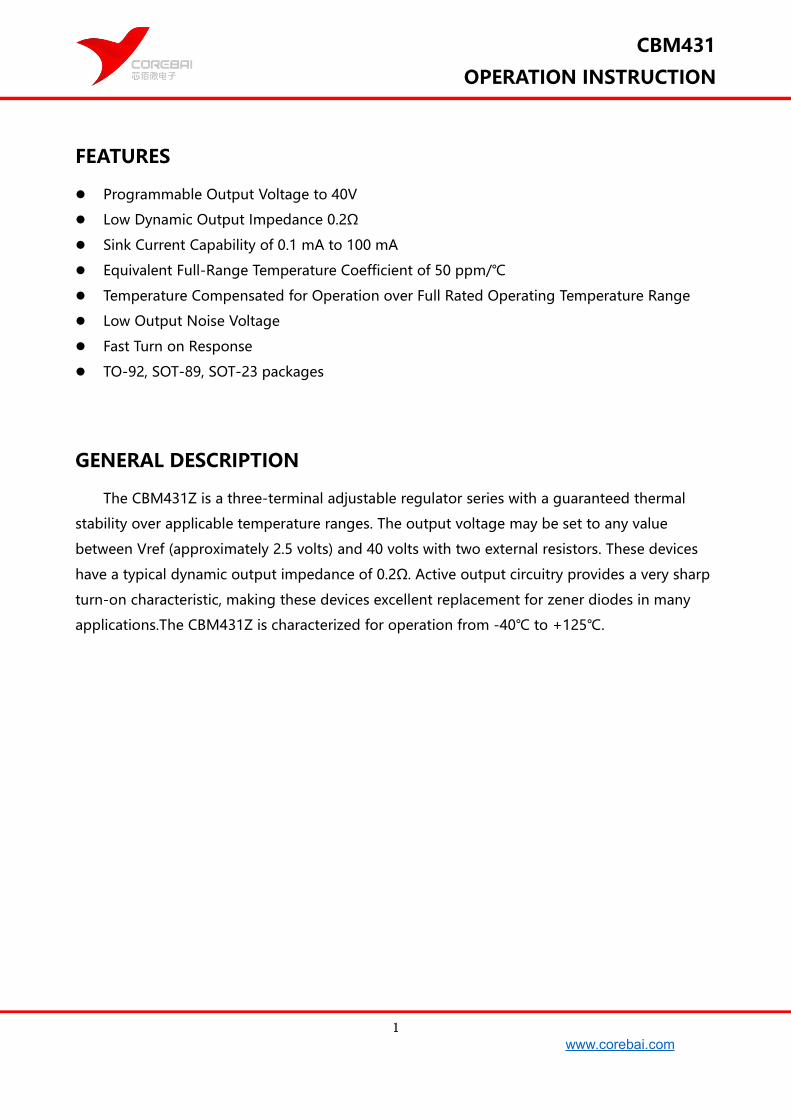
1 www.corebai.com CBM431 OPERATION INSTRUCTION FEATURES Programmable Output Voltage to 40V Low Dynamic Output Impedance 0.2Ω Sink Current Capability of 0.1 mA to 100 mA Equivalent Full-Range Temperature Coefficient of 50 ppm/℃ Temperature Compensated for Operation over Full Rated Operating Temperature Range Low Output Noise Voltage Fast Turn on Response TO-92, SOT-89, SOT-23 packages GENERAL DESCRIPTION The CBM431Z is a three-terminal adjustable regulator series with a guaranteed thermal stability over applicable temperature ranges. The output voltage may be set to any value between Vref (approximately 2.5 volts) and 40 volts with two external resistors. These devices have a typical dynamic output impedance of 0.2Ω. Active output circuitry provides a very sharp turn-on characteristic, making these devices excellent replacement for zener diodes in many applications.The CBM431Z is characterized for operation from -40℃ to +125℃.
Transcript of CBM431 OPERATION INSTRUCTION FEATURESonly hope for stabilizing this circuit is to add a zero....
1
www.corebai.com
CBM431
OPERATION INSTRUCTION
FEATURES
Programmable Output Voltage to 40V
Low Dynamic Output Impedance 0.2Ω
Sink Current Capability of 0.1 mA to 100 mA
Equivalent Full-Range Temperature Coefficient of 50 ppm/
Temperature Compensated for Operation over Full Rated Operating Temperature Range
Low Output Noise Voltage
Fast Turn on Response
TO-92, SOT-89, SOT-23 packages
GENERAL DESCRIPTION
The CBM431Z is a three-terminal adjustable regulator series with a guaranteed thermal
stability over applicable temperature ranges. The output voltage may be set to any value
between Vref (approximately 2.5 volts) and 40 volts with two external resistors. These devices
have a typical dynamic output impedance of 0.2Ω. Active output circuitry provides a very sharp
turn-on characteristic, making these devices excellent replacement for zener diodes in many
applications.The CBM431Z is characterized for operation from -40 to +125.
2
www.corebai.com
CBM431
OPERATION INSTRUCTION
Symbol Functional Block Diagram Equivalent Schematic
ABSOLUTE MAXIMUM RATINGS
(Operating temperature range applies unless otherwise specified)
Characteristic Symbol Value Unit
Cathode Voltage VKA 44 V
Cathode Current Range (Continuous) IK -100 ~ 150 mA
Reference Input Current Range IREF 0.05 ~ 10 mA
Power Dissipation at 25:
TO – 92 Package
(RθJA = 178/W)
SOT Package (RθJA = 625/W)
PD
0.7
0.2
W
W
Junction Temperature Range TJ 0 ~ 150
Operating Temperature Range Tg -40 ~ 125
Storage Temperature Range Tstg -65 ~ 150
* Stresses beyond those listed under “absolute maximum ratings” may cause permanent damage to the device. Theseare stress ratings only, and functional operation of the device at these or any other conditions beyond those indicatedunder “recommended operating conditions” is not implied.Exposure to absolute-maximum-rated conditions for extended periods may affect device reliability.
RECOMMENDED OPERATING CONDITIONS
Characteristic Symbol Min Typ Max Unit
Cathode to Anode Voltage VKA VREF 0.01 40 V
Cathode Current IK 0.5 0.5 100 mA
3
www.corebai.com
CBM431
OPERATION INSTRUCTION
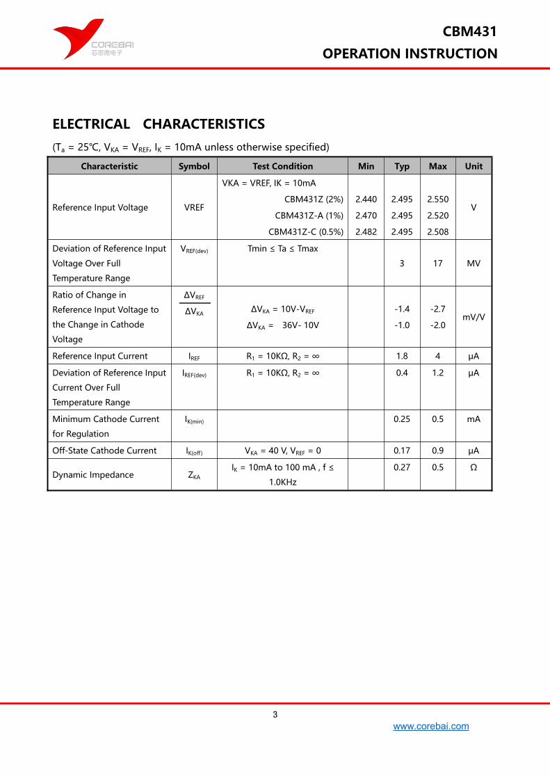
ELECTRICAL CHARACTERISTICS
(Ta = 25, VKA = VREF, IK = 10mA unless otherwise specified)
Characteristic Symbol Test Condition Min Typ Max Unit
Reference Input Voltage VREF
VKA = VREF, IK = 10mA
CBM431Z (2%)
CBM431Z-A (1%)
CBM431Z-C (0.5%)
2.440
2.470
2.482
2.495
2.495
2.495
2.550
2.520
2.508
V
Deviation of Reference Input
Voltage Over Full
Temperature Range
VREF(dev) Tmin ≤ Ta ≤ Tmax
3 17 MV
Ratio of Change in
Reference Input Voltage to
the Change in Cathode
Voltage
∆VREF
∆VKA∆VKA = 10V-VREF
∆VKA = 36V- 10V
-1.4
-1.0
-2.7
-2.0mV/V
Reference Input Current IREF R1 = 10KΩ, R2 = ∞ 1.8 4 μA
Deviation of Reference Input
Current Over Full
Temperature Range
IREF(dev) R1 = 10KΩ, R2 = ∞ 0.4 1.2 μA
Minimum Cathode Current
for Regulation
IK(min) 0.25 0.5 mA
Off-State Cathode Current IK(off) VKA = 40 V, VREF = 0 0.17 0.9 μA
Dynamic Impedance ZKA
IK = 10mA to 100 mA , f ≤
1.0KHz
0.27 0.5 Ω
4
www.corebai.com
CBM431
OPERATION INSTRUCTION
Note :
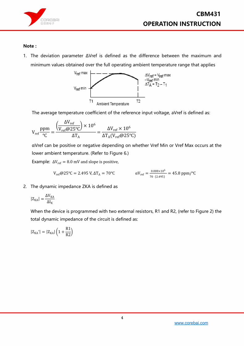
1. The deviation parameter ∆Vref is defined as the difference between the maximum and
minimum values obtained over the full operating ambient temperature range that applies
The average temperature coefficient of the reference input voltage, aVref is defined as:
Vrefppm
=
∆VrefVref@25
× 106
∆TA=
∆Vref × 106
∆TA(Vref@25)
αVref can be positive or negative depending on whether Vref Min or Vref Max occurs at the
lower ambient temperature. (Refer to Figure 6.)
Example: ∆Vref = 8.0 mV and slope is positive,
Vref@25 = 2.495 V, ∆TA = 70 αVref =0.008×10⁶
70(2.495)= 45.8 ppm/
2. The dynamic impedance ZKA is defined as
ZKA =∆VKA∆IK
When the device is programmed with two external resistors, R1 and R2, (refer to Figure 2) the
total dynamic impedance of the circuit is defined as:
ZKA' = ZKA 1 +R1R2
5
www.corebai.com
CBM431
OPERATION INSTRUCTION
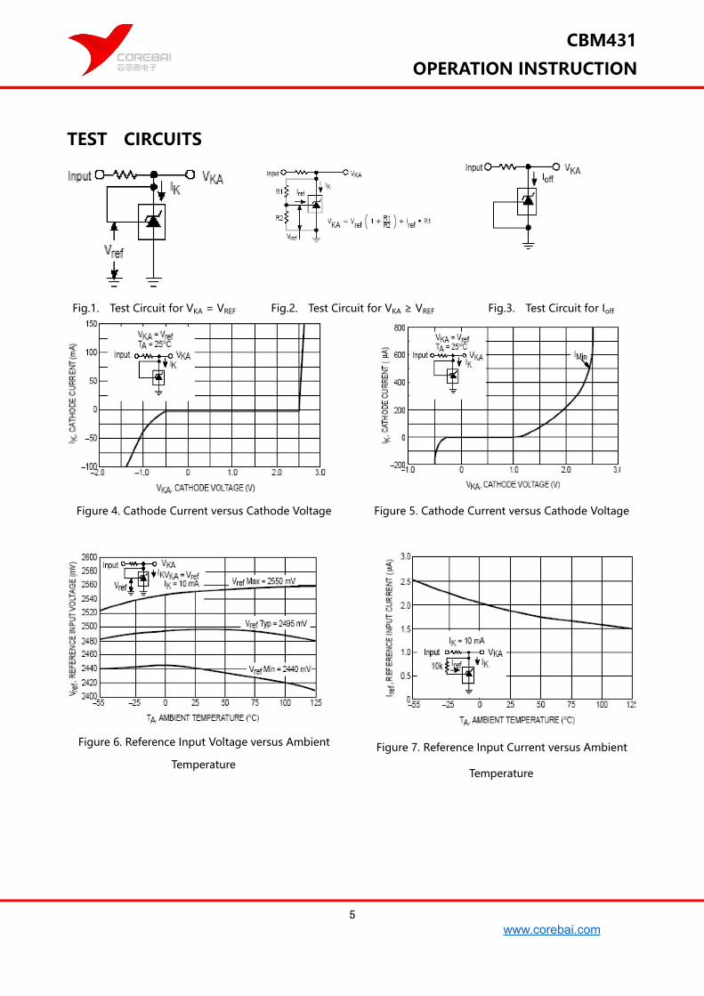
TEST CIRCUITS
Fig.1. Test Circuit for VKA = VREF Fig.2. Test Circuit for VKA ≥ VREF Fig.3. Test Circuit for Ioff
Figure 4. Cathode Current versus Cathode Voltage
Figure 6. Reference Input Voltage versus Ambient
Temperature
Figure 5. Cathode Current versus Cathode Voltage
Figure 7. Reference Input Current versus Ambient
Temperature
6
www.corebai.com
CBM431
OPERATION INSTRUCTION
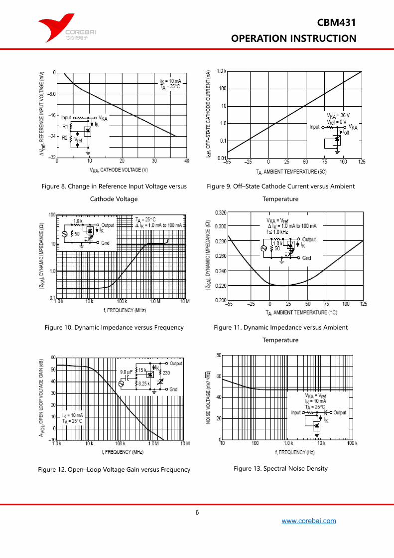
Figure 8. Change in Reference Input Voltage versus
Cathode Voltage
Figure 10. Dynamic Impedance versus Frequency
Figure 12. Open–Loop Voltage Gain versus Frequency
Figure 9. Off–State Cathode Current versus Ambient
Temperature
Figure 11. Dynamic Impedance versus Ambient
Temperature
Figure 13. Spectral Noise Density
7
www.corebai.com
CBM431
OPERATION INSTRUCTION
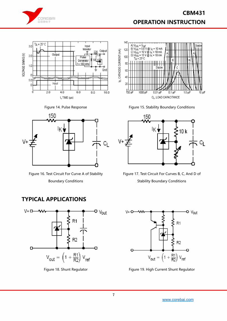
Figure 14. Pulse Response
Figure 16. Test Circuit For Curve A of Stability
Boundary Conditions
Figure 15. Stability Boundary Conditions
Figure 17. Test Circuit For Curves B, C, And D of
Stability Boundary Conditions
TYPICAL APPLICATIONS
Figure 18. Shunt Regulator Figure 19. High Current Shunt Regulator
8
www.corebai.com
CBM431
OPERATION INSTRUCTION
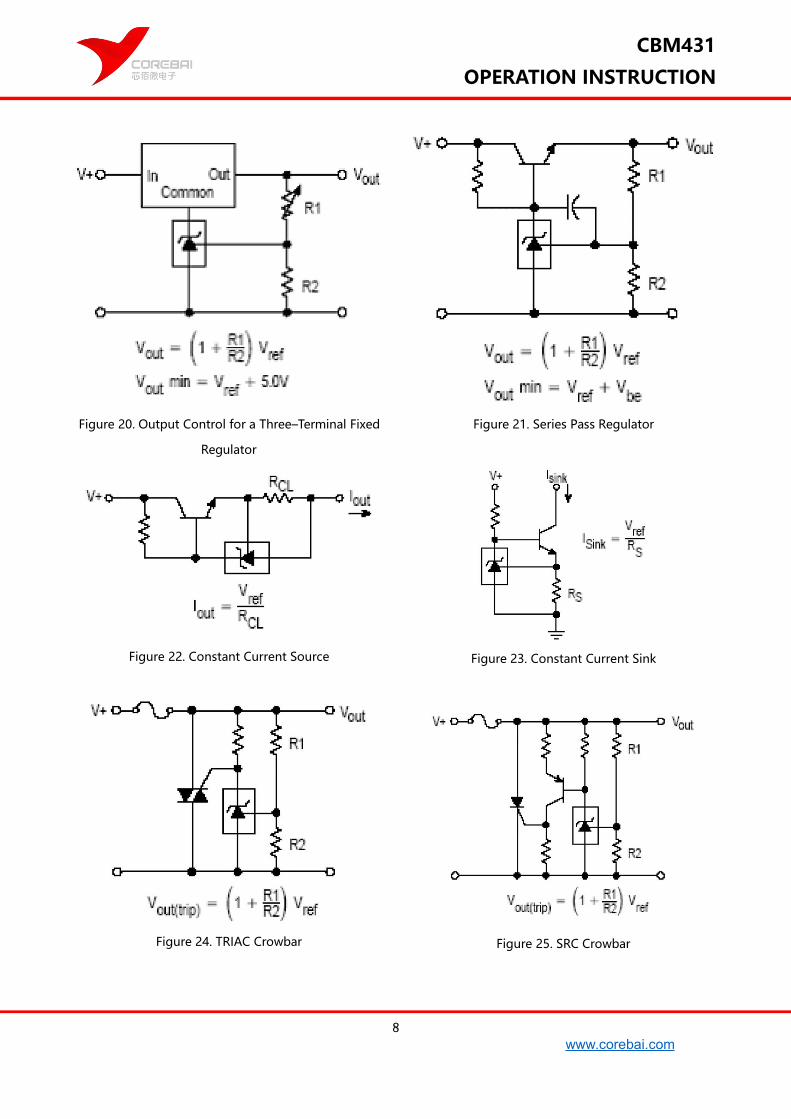
Figure 20. Output Control for a Three–Terminal Fixed
Regulator
Figure 22. Constant Current Source
Figure 24. TRIAC Crowbar
Figure 21. Series Pass Regulator
Figure 23. Constant Current Sink
Figure 25. SRC Crowbar
9
www.corebai.com
CBM431
OPERATION INSTRUCTION
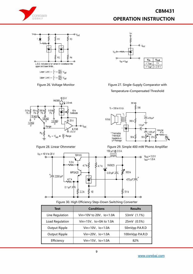
Figure 26. Voltage Monitor
Figure 28. Linear Ohmmeter
Figure 27. Single–Supply Comparator with
Temperature–Compensated Threshold
Figure 29. Simple 400 mW Phono Amplifier
Figure 30. High Efficiency Step–Down Switching Converter
Test Conditions Results
Line Regulation Vin=10V to 20V,Io=1.0A 53mV(1.1%)
Load Regulation Vin=15V,Io=0A to 1.0A 25mV(0.5%)
Output Ripple Vin=10V,Io=1.0A 50mVpp P.A.R.D
Output Ripple Vin=20V,Io=1.0A 100mVpp P.A.R.D
Efficiency Vin=15V,Io=1.0A 82%
10
www.corebai.com
CBM431
OPERATION INSTRUCTION
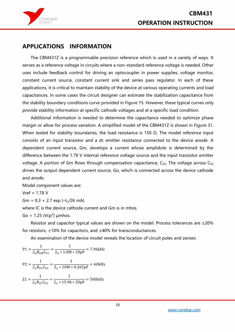
APPLICATIONS INFORMATION
The CBM431Z is a programmable precision reference which is used in a variety of ways. It
serves as a reference voltage in circuits where a non–standard reference voltage is needed. Other
uses include feedback control for driving an optocoupler in power supplies, voltage monitor,
constant current source, constant current sink and series pass regulator. In each of these
applications, it is critical to maintain stability of the device at various operating currents and load
capacitances. In some cases the circuit designer can estimate the stabilization capacitance from
the stability boundary conditions curve provided in Figure 15. However, these typical curves only
provide stability information at specific cathode voltages and at a specific load condition.
Additional information is needed to determine the capacitance needed to optimize phase
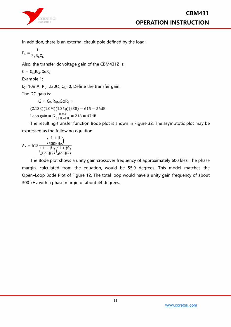
margin or allow for process variation. A simplified model of the CBM431Z is shown in Figure 31.
When tested for stability boundaries, the load resistance is 150 Ω. The model reference input
consists of an input transistor and a dc emitter resistance connected to the device anode. A
dependent current source, Gm, develops a current whose amplidute is determined by the
difference between the 1.78 V internal reference voltage source and the input transistor emitter
voltage. A portion of Gm flows through compensation capacitance, CP2. The voltage across CP2
drives the output dependent current source, Go, which is connected across the device cathode
and anode.
Model component values are:
Vref = 1.78 V
Gm = 0.3 + 2.7 exp (–IC/26 mA)
where IC is the device cathode current and Gm is in mhos
Go = 1.25 (Vcp2) µmhos.
Resistor and capacitor typical values are shown on the model. Process tolerances are ±20%
for resistors, ±10% for capacitors, and ±40% for transconductances.
An examination of the device model reveals the location of circuit poles and zeroes:
P1 =1
2πRGMCP1=
12π ∗ 1.0M ∗ 20pF
= 7.96kHz
P2 =1
2πRP2CP2=
12π ∗ 10M ∗ 0.265pF
= 60kHz
Z1 =1
2πRZ1CP1=
12π ∗ 15.9k ∗ 20pF
= 500kHz
11
www.corebai.com
CBM431
OPERATION INSTRUCTION
In addition, there is an external circuit pole defined by the load:
PL =1
2πRLCL
Also, the transfer dc voltage gain of the CBM431Z is:
G = GMRGMGoRL
Example 1:
IC=10mA, RL=230Ω, CL=0, Define the transfer gain.
The DC gain is:
G = GMRGMGoRL =
(2.138)(1.0M)(1.25μ)(230) = 615 = 56dB
Loop gain = G 8.25k8.25k+15k
= 218 = 47dB
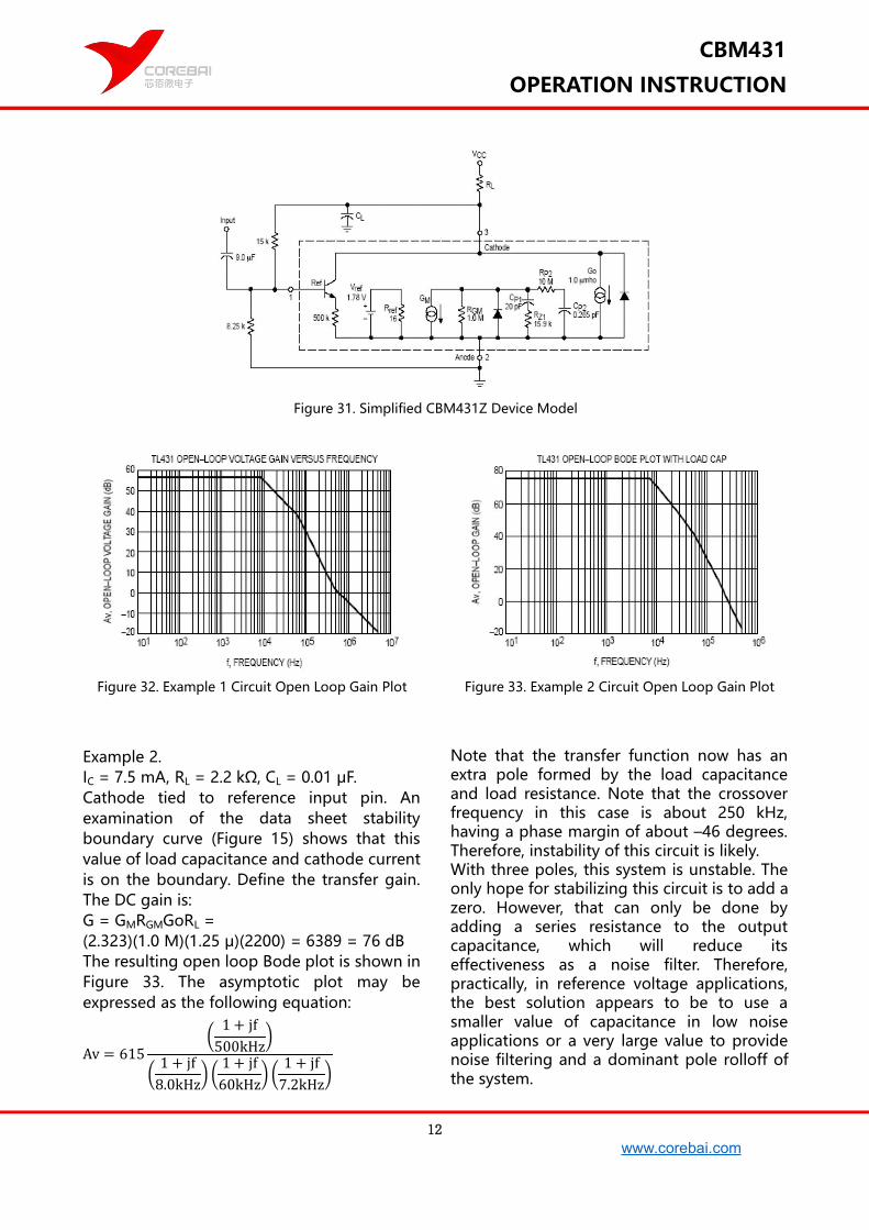
The resulting transfer function Bode plot is shown in Figure 32. The asymptotic plot may be
expressed as the following equation:
Av = 615
1 + jf500kHz
1 + jf8.0kHz
1 + jf60kHz
The Bode plot shows a unity gain crossover frequency of approximately 600 kHz. The phase
margin, calculated from the equation, would be 55.9 degrees. This model matches the
Open–Loop Bode Plot of Figure 12. The total loop would have a unity gain frequency of about
300 kHz with a phase margin of about 44 degrees.
12
www.corebai.com
CBM431
OPERATION INSTRUCTION
Figure 31. Simplified CBM431Z Device Model
Figure 32. Example 1 Circuit Open Loop Gain Plot Figure 33. Example 2 Circuit Open Loop Gain Plot
Example 2.IC = 7.5 mA, RL = 2.2 kΩ, CL = 0.01 μF.Cathode tied to reference input pin. Anexamination of the data sheet stabilityboundary curve (Figure 15) shows that thisvalue of load capacitance and cathode currentis on the boundary. Define the transfer gain.The DC gain is:G = GMRGMGoRL =(2.323)(1.0 M)(1.25 μ)(2200) = 6389 = 76 dBThe resulting open loop Bode plot is shown inFigure 33. The asymptotic plot may beexpressed as the following equation:
Av = 615
1 + jf500kHz
1 + jf8.0kHz
1 + jf60kHz
1 + jf7.2kHz
Note that the transfer function now has anextra pole formed by the load capacitanceand load resistance. Note that the crossoverfrequency in this case is about 250 kHz,having a phase margin of about –46 degrees.Therefore, instability of this circuit is likely.With three poles, this system is unstable. Theonly hope for stabilizing this circuit is to add azero. However, that can only be done byadding a series resistance to the outputcapacitance, which will reduce itseffectiveness as a noise filter. Therefore,practically, in reference voltage applications,the best solution appears to be to use asmaller value of capacitance in low noiseapplications or a very large value to providenoise filtering and a dominant pole rolloff ofthe system.
13
www.corebai.com
CBM431
OPERATION INSTRUCTION
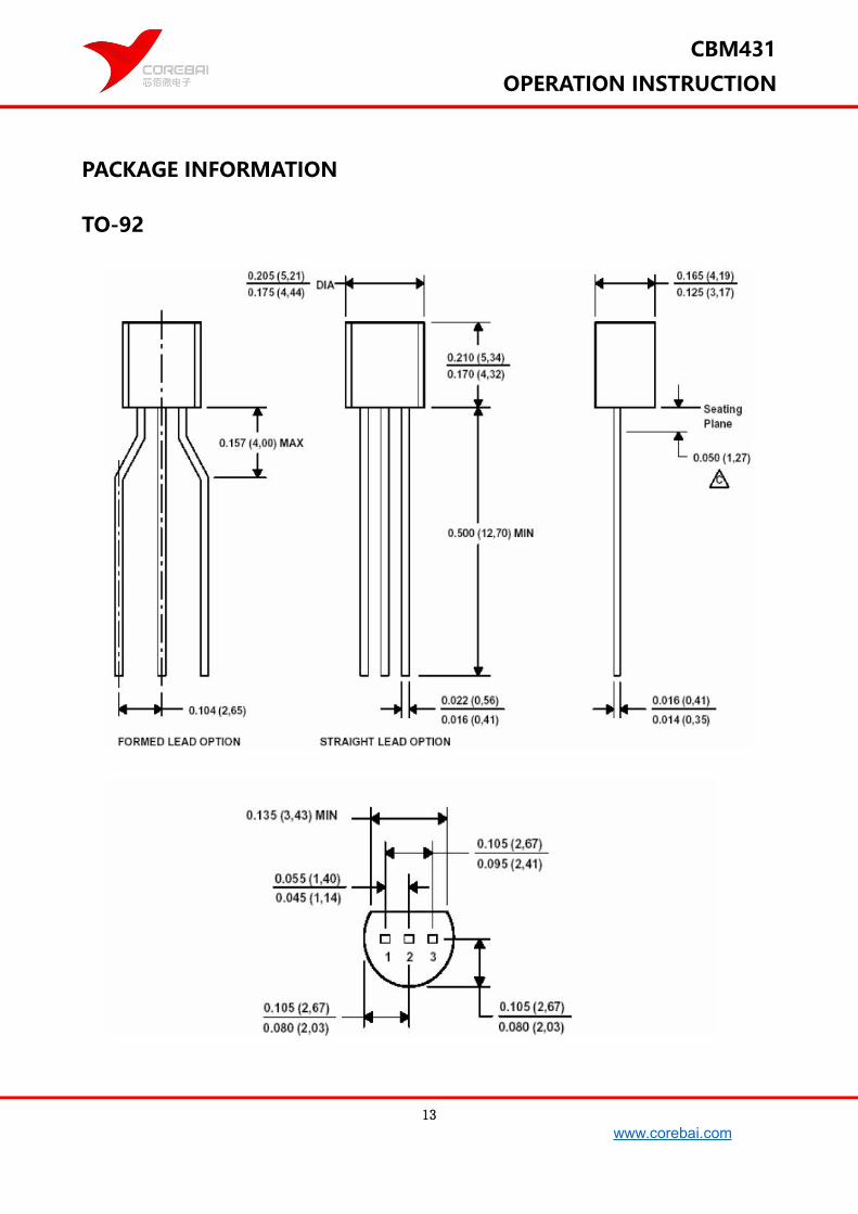
PACKAGE INFORMATION
TO-92
14
www.corebai.com
CBM431
OPERATION INSTRUCTION
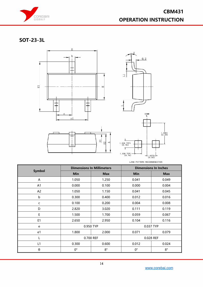
SOT-23-3L
SymbolDimensions In Millimeters Dimensions In Inches
Min Max Min Max
A 1.050 1.250 0.041 0.049
A1 0.000 0.100 0.000 0.004
A2 1.050 1.150 0.041 0.045
b 0.300 0.400 0.012 0.016
c 0.100 0.200 0.004 0.008
D 2.820 3.020 0.111 0.119
E 1.500 1.700 0.059 0.067
E1 2.650 2.950 0.104 0.116
e 0.950 TYP 0.037 TYP
e1 1.800 2.000 0.071 0.079
L 0.700 REF 0.028 REF
L1 0.300 0.600 0.012 0.024
θ 0° 8° 0° 8°
15
www.corebai.com
CBM431
OPERATION INSTRUCTION
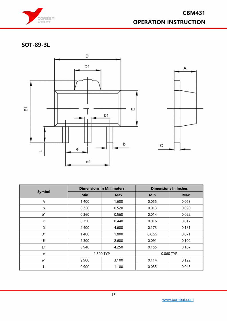
SOT-89-3L
SymbolDimensions In Millimeters Dimensions In Inches
Min Max Min Max
A 1.400 1.600 0.055 0.063
b 0.320 0.520 0.013 0.020
b1 0.360 0.560 0.014 0.022
c 0.350 0.440 0.016 0.017
D 4.400 4.600 0.173 0.181
D1 1.400 1.800 0.0.55 0.071
E 2.300 2.600 0.091 0.102
E1 3.940 4.250 0.155 0.167
e 1.500 TYP 0.060 TYP
e1 2.900 3.100 0.114 0.122
L 0.900 1.100 0.035 0.043
16
www.corebai.com
CBM431
OPERATION INSTRUCTION
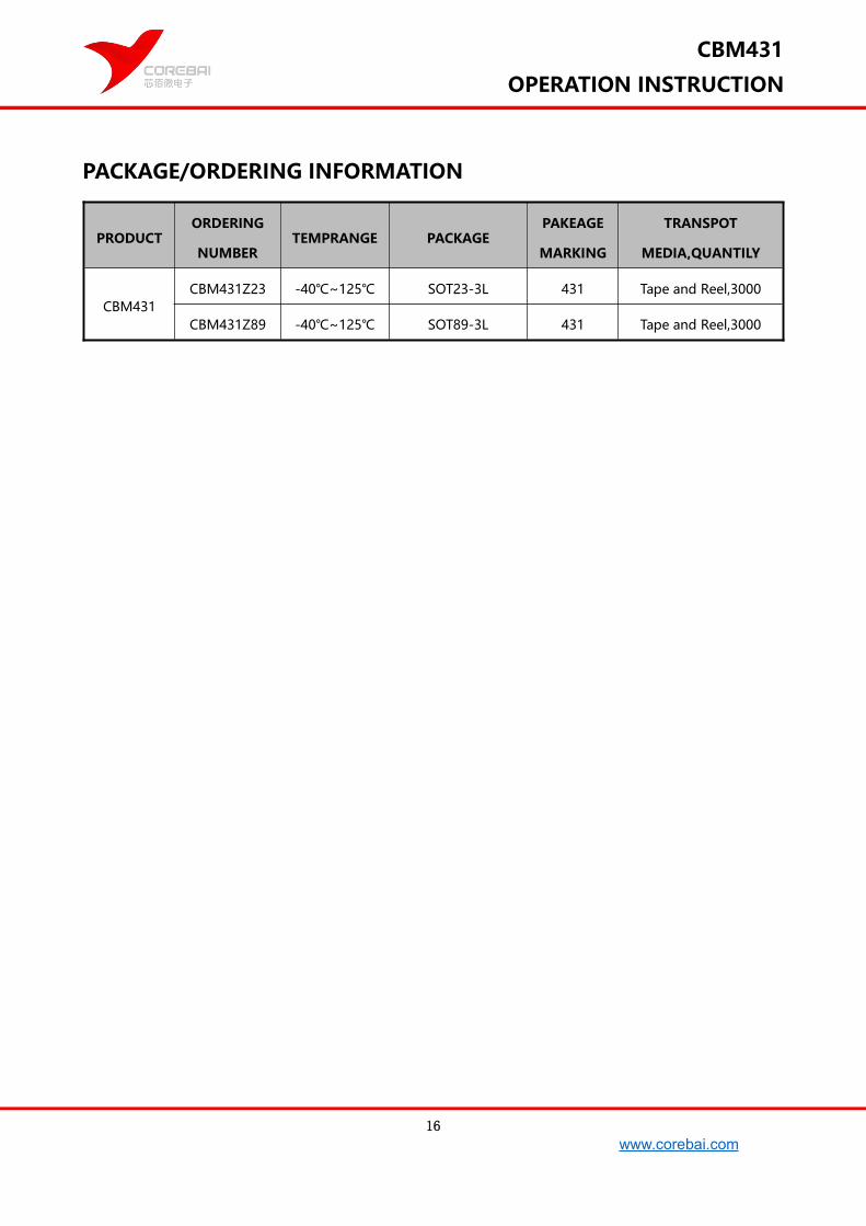
PACKAGE/ORDERING INFORMATION
PRODUCTORDERING
NUMBERTEMPRANGE PACKAGE
PAKEAGE
MARKING
TRANSPOT
MEDIA,QUANTILY
CBM431CBM431Z23 -40~125 SOT23-3L 431 Tape and Reel,3000
CBM431Z89 -40~125 SOT89-3L 431 Tape and Reel,3000