Antoine JUNIQUE, Gabriele FIORENZA, Satoshi YANO 1 Laser soldering test 11/03/2014.
9
Antoine JUNIQUE, Gabriele FIORENZA, Satoshi YANO 1 Laser soldering test 11/03/2014
-
Upload
claud-oneal -
Category
Documents
-
view
216 -
download
1
Transcript of Antoine JUNIQUE, Gabriele FIORENZA, Satoshi YANO 1 Laser soldering test 11/03/2014.
Antoine JUNIQUE, Gabriele FIORENZA, Satoshi YANO 1
Laser soldering test
11/03/2014
Antoine JUNIQUE, Gabriele FIORENZA, Satoshi YANO 211/03/2014
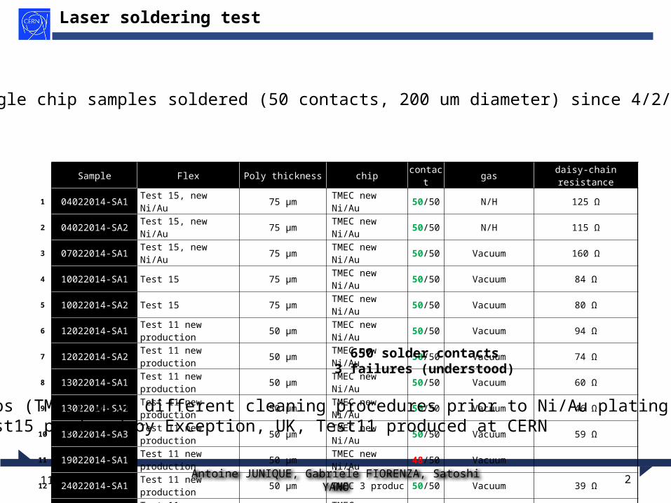
Sample Flex Poly thickness chip contact gas daisy-chain resistance1 04022014-SA1 Test 15, new Ni/Au 75 µm TMEC new Ni/Au 50/50 N/H 125 Ω2 04022014-SA2 Test 15, new Ni/Au 75 µm TMEC new Ni/Au 50/50 N/H 115 Ω3 07022014-SA1 Test 15, new Ni/Au 75 µm TMEC new Ni/Au 50/50 Vacuum 160 Ω4 10022014-SA1 Test 15 75 µm TMEC new Ni/Au 50/50 Vacuum 84 Ω5 10022014-SA2 Test 15 75 µm TMEC new Ni/Au 50/50 Vacuum 80 Ω6 12022014-SA1 Test 11 new production 50 µm TMEC new Ni/Au 50/50 Vacuum 94 Ω7 12022014-SA2 Test 11 new production 50 µm TMEC new Ni/Au 50/50 Vacuum 74 Ω8 13022014-SA1 Test 11 new production 50 µm TMEC new Ni/Au 50/50 Vacuum 60 Ω9 13022014-SA2 Test 11 new production 50 µm TMEC new Ni/Au 50/50 Vacuum 46 Ω10 13022014-SA3 Test 11 new production 50 µm TMEC new Ni/Au 50/50 Vacuum 59 Ω11 19022014-SA1 Test 11 new production 50 µm TMEC new Ni/Au 48/50 Vacuum 12 24022014-SA1 Test 11 new production 50 µm TMEC 3 produc 50/50 Vacuum 39 Ω13 26022014-SA1 Test 11 new production 50 µm TMEC new Ni/Au 49/50 Vacuum
Laser soldering test
Single chip samples soldered (50 contacts, 200 um diameter) since 4/2/2014:
Pad-chips (TMEC) with different cleaning procedures prior to Ni/Au plating at CERNFPC: Test15 produced by Exception, UK, Test11 produced at CERN
650 solder contacts3 failures (understood)
Antoine JUNIQUE, Gabriele FIORENZA, Satoshi YANO 311/03/2014
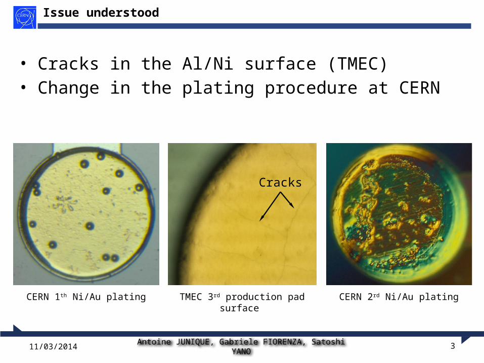
Issue understood
• Cracks in the Al/Ni surface (TMEC)• Change in the plating procedure at CERN
TMEC 3rd production pad surface CERN 1th Ni/Au plating CERN 2rd Ni/Au plating
Cracks
0.025 1.825 3.625 5.425 7.225 9.025 10.8250
100
200
300
400
500
600
0
10
20
30
40
50
60
70
80
90
100
CERN Profile 139
ATempCtrlOut
Time (s)
Tem
pera
ture
(C°)
Antoine JUNIQUE, Gabriele FIORENZA, Satoshi YANO 411/03/2014
10 s @ 250 C°
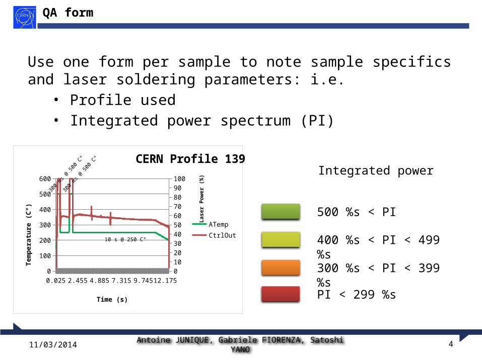
Use one form per sample to note sample specifics and laser soldering parameters: i.e.
• Profile used• Integrated power spectrum (PI)
QA form
500 %s < PI
400 %s < PI < 499 %s
300 %s < PI < 399 %s
PI < 299 %s
Integrated power
300
ms
@ 5
00 C
°
300
ms
@ 5
00 C
°
Las
er P
ow
er (
%)
Antoine JUNIQUE, Gabriele FIORENZA, Satoshi YANO 5
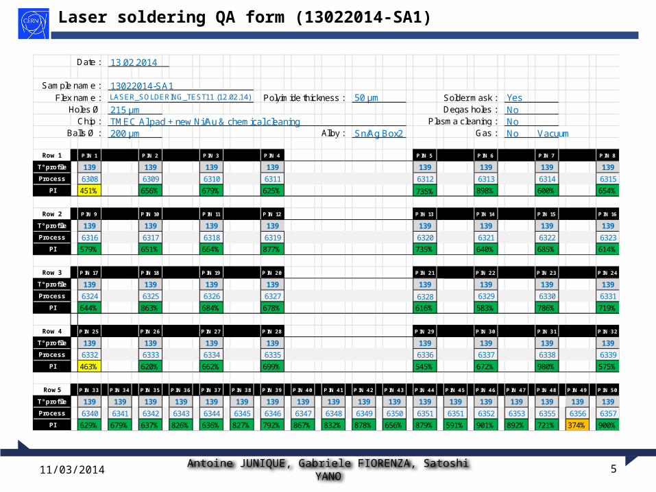
Date : 13.02.2014
Sample name : 13022014-SA1Flex name : LASER_SOLDERING_TEST11 (12.02.14) Polyimide thickness : 50 µm Solder mask : Yes
Holes Ø 215 µm Degas holes : NoChip : TMEC Al pad + new Ni/Au & chemical cleaning Plasma cleaning : No
Balls Ø : 200 µm Alloy : Sn/Ag Box2 Gas : No Vacuum
Row 1 PIN 1 PIN 2 PIN 3 PIN 4 PIN 5 PIN 6 PIN 7 PIN 8
T° profile 139 139 139 139 139 139 139 139
Process 6308 6309 6310 6311 6312 6313 6314 6315
PI 451% 656% 679% 625% 735% 898% 600% 654%
Row 2 PIN 9 PIN 10 PIN 11 PIN 12 PIN 13 PIN 14 PIN 15 PIN 16
T° profile 139 139 139 139 139 139 139 139
Process 6316 6317 6318 6319 6320 6321 6322 6323
PI 579% 651% 664% 877% 735% 640% 685% 614%
Row 3 PIN 17 PIN 18 PIN 19 PIN 20 PIN 21 PIN 22 PIN 23 PIN 24
T° profile 139 139 139 139 139 139 139 139
Process 6324 6325 6326 6327 6328 6329 6330 6331
PI 644% 863% 684% 678% 616% 583% 786% 719%
Row 4 PIN 25 PIN 26 PIN 27 PIN 28 PIN 29 PIN 30 PIN 31 PIN 32
T° profile 139 139 139 139 139 139 139 139
Process 6332 6333 6334 6335 6336 6337 6338 6339
PI 463% 620% 662% 699% 545% 672% 980% 575%
Row5 PIN 33 PIN 34 PIN 35 PIN 36 PIN 37 PIN 38 PIN 39 PIN 40 PIN 41 PIN 42 PIN 43 PIN 44 PIN 45 PIN 46 PIN 47 PIN 48 PIN 49 PIN 50
T° profile 139 139 139 139 139 139 139 139 139 139 139 139 139 139 139 139 139 139
Process 6340 6341 6342 6343 6344 6345 6346 6347 6348 6349 6350 6351 6351 6352 6353 6355 6356 6357
PI 629% 679% 637% 826% 636% 827% 792% 867% 832% 878% 656% 879% 591% 901% 892% 721% 374% 900%
11/03/2014
Laser soldering QA form (13022014-SA1)
Antoine JUNIQUE, Gabriele FIORENZA, Satoshi YANO 6
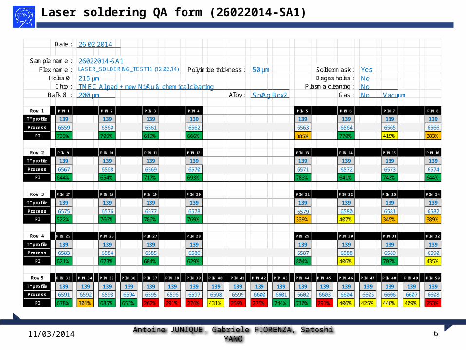
Date : 26.02.2014
Sample name : 26022014-SA1Flex name : LASER_SOLDERING_TEST11 (12.02.14) Polyimide thickness : 50 µm Solder mask : Yes
Holes Ø 215 µm Degas holes : NoChip : TMEC Al pad + new Ni/Au & chemical cleaning Plasma cleaning : No
Balls Ø : 200 µm Alloy : Sn/Ag Box2 Gas : No Vacuum
Row 1 PIN 1 P IN 2 P IN 3 P IN 4 P IN 5 P IN 6 P IN 7 P IN 8
T° profile 139 139 139 139 139 139 139 139
Process 6559 6560 6561 6562 6563 6564 6565 6566
PI 739% 709% 619% 666% 385% 770% 415% 383%
Row 2 PIN 9 P IN 10 PIN 11 PIN 12 PIN 13 PIN 14 PIN 15 PIN 16
T° profile 139 139 139 139 139 139 139 139
Process 6567 6568 6569 6570 6571 6572 6573 6574
PI 644% 654% 717% 693% 783% 641% 743% 644%
Row 3 PIN 17 PIN 18 PIN 19 PIN 20 PIN 21 PIN 22 PIN 23 PIN 24
T° profile 139 139 139 139 139 139 139 139
Process 6575 6576 6577 6578 6579 6580 6581 6582
PI 522% 766% 786% 769% 339% 407% 345% 389%
Row 4 PIN 25 PIN 26 PIN 27 PIN 28 PIN 29 PIN 30 PIN 31 PIN 32
T° profile 139 139 139 139 139 139 139 139
Process 6583 6584 6585 6586 6587 6588 6589 6590
PI 621% 673% 604% 629% 804% 406% 703% 435%
Row5 PIN 33 PIN 34 PIN 35 PIN 36 PIN 37 PIN 38 PIN 39 PIN 40 PIN 41 PIN 42 PIN 43 PIN 44 PIN 45 PIN 46 PIN 47 PIN 48 PIN 49 PIN 50
T° profile 139 139 139 139 139 139 139 139 139 139 139 139 139 139 139 139 139 139
Process 6591 6592 6593 6594 6595 6596 6597 6598 6599 6600 6601 6602 6603 6604 6605 6606 6607 6608
PI 678% 301% 685% 653% 262% 291% 276% 431% 259% 275% 744% 710% 291% 406% 425% 448% 409% 253%
11/03/2014
Laser soldering QA form (26022014-SA1)
Antoine JUNIQUE, Gabriele FIORENZA, Satoshi YANO 7
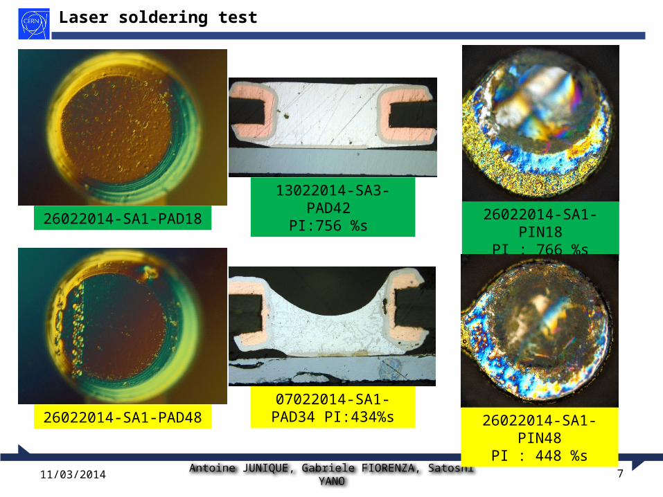
26022014-SA1-PAD18
26022014-SA1-PAD48
13022014-SA3-PAD42 PI:756 %s
07022014-SA1-PAD34 PI:434%s
26022014-SA1-PIN18PI : 766 %s
26022014-SA1-PIN48PI : 448 %s
11/03/2014
Laser soldering test
Antoine JUNIQUE, Gabriele FIORENZA, Satoshi YANO 8
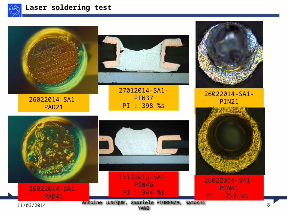
26022014-SA1-PAD2126022014-SA1-PIN21
PI : 339 %s
26022014-SA1-PAD4126022014-SA1-PIN41
PI : 259 %s
27012014-SA1-PIN37PI : 398 %s
13122013-SA1-PIN46PI : 344 %s
11/03/2014
Laser soldering test
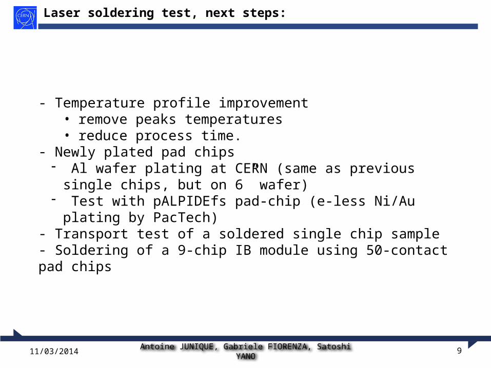
Antoine JUNIQUE, Gabriele FIORENZA, Satoshi YANO 911/03/2014
Laser soldering test, next steps:
- Temperature profile improvement• remove peaks temperatures• reduce process time.
- Newly plated pad chips- Al wafer plating at CERN (same as previous single chips, but
on 6” wafer)- Test with pALPIDEfs pad-chip (e-less Ni/Au plating by
PacTech)- Transport test of a soldered single chip sample- Soldering of a 9-chip IB module using 50-contact pad chips