AD8015 Wideband/Differential Output Transimpedance a Wideband/Differential Output Transimpedance...
8
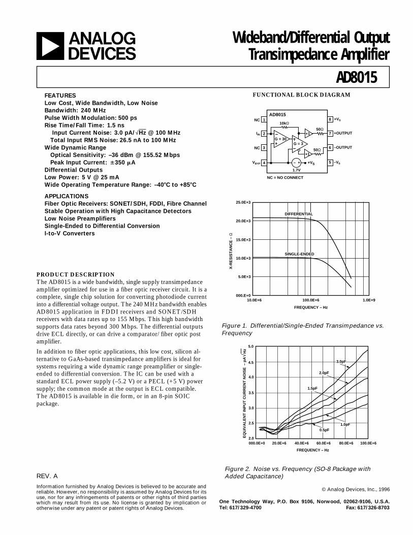
FUNCTIONAL BLOCK DIAGRAM 10kΩ 5 6 7 8 4 3 2 1 AD8015 50Ω +1 NC I IN NC V BYP –V S –OUTPUT +OUTPUT +V S G = 3 G = 30 NC = NO CONNECT 50Ω +1 – + +V S 1.7V 25.0E+3 20.0E+3 000.E+0 10.0E+6 100.0E+6 1.0E+9 15.0E+3 10.0E+3 5.0E+3 FREQUENCY – Hz X-RESISTANCE – Ω DIFFERENTIAL SINGLE-ENDED Figure 1. Differential/Single-Ended Transimpedance vs. Frequency 5.0 4.5 4.0 3.5 3.0 2.5 2.0 100.0E+6 20.0E+6 000.0E+0 80.0E+6 60.0E+6 40.0E+6 FREQUENCY – Hz EQUIVALENT INPUT CURRENT NOISE – pA√ Hz 3.0pF 2.0pF 1.5pF 1.0pF 0.5pF Figure 2. Noise vs. Frequency (SO-8 Package with Added Capacitance) REV. A Information furnished by Analog Devices is believed to be accurate and reliable. However, no responsibility is assumed by Analog Devices for its use, nor for any infringements of patents or other rights of third parties which may result from its use. No license is granted by implication or otherwise under any patent or patent rights of Analog Devices. a Wideband/Differential Output Transimpedance Amplifier AD8015 FEATURES Low Cost, Wide Bandwidth, Low Noise Bandwidth: 240 MHz Pulse Width Modulation: 500 ps Rise Time/Fall Time: 1.5 ns Input Current Noise: 3.0 pA/√ Hz @ 100 MHz Total Input RMS Noise: 26.5 nA to 100 MHz Wide Dynamic Range Optical Sensitivity: –36 dBm @ 155.52 Mbps Peak Input Current: 6350 mA Differential Outputs Low Power: 5 V @ 25 mA Wide Operating Temperature Range: –408C to +858C APPLICATIONS Fiber Optic Receivers: SONET/SDH, FDDI, Fibre Channel Stable Operation with High Capacitance Detectors Low Noise Preamplifiers Single-Ended to Differential Conversion I-to-V Converters PRODUCT DESCRIPTION The AD8015 is a wide bandwidth, single supply transimpedance amplifier optimized for use in a fiber optic receiver circuit. It is a complete, single chip solution for converting photodiode current into a differential voltage output. The 240 MHz bandwidth enables AD8015 application in FDDI receivers and SONET/SDH receivers with data rates up to 155 Mbps. This high bandwidth supports data rates beyond 300 Mbps. The differential outputs drive ECL directly, or can drive a comparator/ fiber optic post amplifier. In addition to fiber optic applications, this low cost, silicon al- ternative to GaAs-based transimpedance amplifiers is ideal for systems requiring a wide dynamic range preamplifier or single- ended to differential conversion. The IC can be used with a standard ECL power supply (–5.2 V) or a PECL (+5 V) power supply; the common mode at the output is ECL compatible. The AD8015 is available in die form, or in an 8-pin SOIC package. © Analog Devices, Inc., 1996 One Technology Way, P.O. Box 9106, Norwood, 02062-9106, U.S.A. Tel: 617/329-4700 Fax: 617/326-8703
Transcript of AD8015 Wideband/Differential Output Transimpedance a Wideband/Differential Output Transimpedance...
FUNCTIONAL BLOCK DIAGRAM
10kΩ
5
6
7
8
4
3
2
1AD8015
50Ω+1
NC
IIN
NC
VBYP –VS
–OUTPUT
+OUTPUT
+VS
G = 3G = 30
NC = NO CONNECT
50Ω+1
– + +VS
1.7V
25.0E+3
20.0E+3
000.E+010.0E+6 100.0E+6 1.0E+9
15.0E+3
10.0E+3
5.0E+3
FREQUENCY – Hz
X-R
ES
IST
AN
CE
– Ω
DIFFERENTIAL
SINGLE-ENDED
Figure 1. Differential/Single-Ended Transimpedance vs.Frequency
5.0
4.5
4.0
3.5
3.0
2.5
2.0100.0E+620.0E+6000.0E+0 80.0E+660.0E+640.0E+6
FREQUENCY – Hz
EQ
UIV
AL
EN
T IN
PU
T C
UR
RE
NT
NO
ISE
– p
A√ H
z
3.0pF
2.0pF
1.5pF
1.0pF0.5pF
Figure 2. Noise vs. Frequency (SO-8 Package withAdded Capacitance)REV. A
Information furnished by Analog Devices is believed to be accurate andreliable. However, no responsibility is assumed by Analog Devices for itsuse, nor for any infringements of patents or other rights of third partieswhich may result from its use. No license is granted by implication orotherwise under any patent or patent rights of Analog Devices.
a Wideband/Differential OutputTransimpedance Amplifier
AD8015FEATURES
Low Cost, Wide Bandwidth, Low Noise
Bandwidth: 240 MHz
Pulse Width Modulation: 500 ps
Rise Time/Fall Time: 1.5 ns
Input Current Noise: 3.0 pA/√Hz @ 100 MHz
Total Input RMS Noise: 26.5 nA to 100 MHz
Wide Dynamic Range
Optical Sensitivity: –36 dBm @ 155.52 Mbps
Peak Input Current: 6350 mA
Differential Outputs
Low Power: 5 V @ 25 mA
Wide Operating Temperature Range: –408C to +858C
APPLICATIONS
Fiber Optic Receivers: SONET/SDH, FDDI, Fibre Channel
Stable Operation with High Capacitance Detectors
Low Noise Preamplifiers
Single-Ended to Differential Conversion
I-to-V Converters
PRODUCT DESCRIPTIONThe AD8015 is a wide bandwidth, single supply transimpedanceamplifier optimized for use in a fiber optic receiver circuit. It is acomplete, single chip solution for converting photodiode currentinto a differential voltage output. The 240 MHz bandwidth enablesAD8015 application in FDDI receivers and SONET/SDHreceivers with data rates up to 155 Mbps. This high bandwidthsupports data rates beyond 300 Mbps. The differential outputsdrive ECL directly, or can drive a comparator/ fiber optic postamplifier.
In addition to fiber optic applications, this low cost, silicon al-ternative to GaAs-based transimpedance amplifiers is ideal forsystems requiring a wide dynamic range preamplifier or single-ended to differential conversion. The IC can be used with astandard ECL power supply (–5.2 V) or a PECL (+5 V) powersupply; the common mode at the output is ECL compatible.The AD8015 is available in die form, or in an 8-pin SOICpackage.
© Analog Devices, Inc., 1996
One Technology Way, P.O. Box 9106, Norwood, 02062-9106, U.S.A.
Tel: 617/329-4700 Fax: 617/326-8703
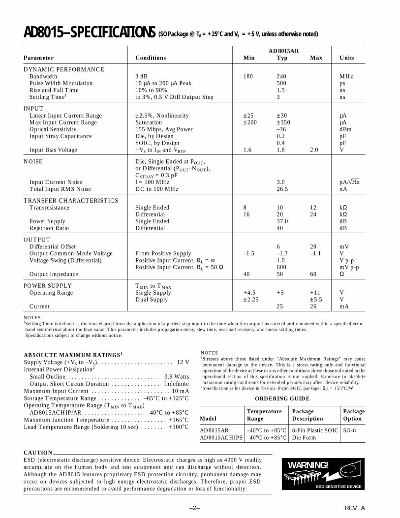
AD8015–SPECIFICATIONS
REV. A–2–
(SO Package @ TA = +258C and VS = +5 V, unless otherwise noted)
AD8015ARParameter Conditions Min Typ Max Units
DYNAMIC PERFORMANCEBandwidth 3 dB 180 240 MHzPulse Width Modulation 10 µA to 200 µA Peak 500 psRise and Fall Time 10% to 90% 1.5 nsSettling Time1 to 3%, 0.5 V Diff Output Step 3 ns
INPUTLinear Input Current Range ±2.5%, Nonlinearity ±25 ±30 µAMax Input Current Range Saturation ±200 ±350 µAOptical Sensitivity 155 Mbps, Avg Power –36 dBmInput Stray Capacitance Die, by Design 0.2 pF
SOIC, by Design 0.4 pFInput Bias Voltage +VS to IIN and VBYP 1.6 1.8 2.0 V
NOISE Die, Single Ended at POUT,or Differential (POUT–NOUT),CSTRAY = 0.3 pF
Input Current Noise f = 100 MHz 3.0 pA/√HzTotal Input RMS Noise DC to 100 MHz 26.5 nA
TRANSFER CHARACTERISTICSTransresistance Single Ended 8 10 12 kΩ
Differential 16 20 24 kΩPower Supply Single Ended 37.0 dBRejection Ratio Differential 40 dB
OUTPUTDifferential Offset 6 20 mVOutput Common-Mode Voltage From Positive Supply –1.5 –1.3 –1.1 VVoltage Swing (Differential) Positive Input Current, RL = ∞ 1.0 V p-p
Positive Input Current, RL = 50 Ω 600 mV p-pOutput Impedance 40 50 60 Ω
POWER SUPPLY TMIN to TMAXOperating Range Single Supply +4.5 +5 +11 V
Dual Supply ±2.25 ±5.5 VCurrent 25 26 mA
NOTES1Settling Time is defined as the time elapsed from the application of a perfect step input to the time when the output has entered and remained within a specified errorband symmetrical about the final value. This parameter includes propagation delay, slew time, overload recovery, and linear settling times.Specifications subject to change without notice.
WARNING!
ESD SENSITIVE DEVICE
CAUTIONESD (electrostatic discharge) sensitive device. Electrostatic charges as high as 4000 V readilyaccumulate on the human body and test equipment and can discharge without detection.Although the AD8015 features proprietary ESD protection circuitry, permanent damage mayoccur on devices subjected to high energy electrostatic discharges. Therefore, proper ESDprecautions are recommended to avoid performance degradation or loss of functionality.
ABSOLUTE MAXIMUM RATINGS1
Supply Voltage (+VS to –VS). . . . . . . . . . . . . . . . . . . . . . . 12 VInternal Power Dissipation2
Small Outline . . . . . . . . . . . . . . . . . . . . . . . . . . . . 0.9 WattsOutput Short Circuit Duration . . . . . . . . . . . . . . . Indefinite
Maximum Input Current . . . . . . . . . . . . . . . . . . . . . . . . 10 mAStorage Temperature Range . . . . . . . . . . . . –65°C to +125°COperating Temperature Range (TMIN to TMAX)
AD8015ACHIP/AR . . . . . . . . . . . . . . . . . . –40°C to +85°CMaximum Junction Temperature . . . . . . . . . . . . . . . . . +165°CLead Temperature Range (Soldering 10 sec) . . . . . . . . +300°C
NOTES1Stresses above those listed under “Absolute Maximum Ratings” may causepermanent damage to the device. This is a stress rating only and functionaloperation of the device at these or any other conditions above those indicated in theoperational section of this specification is not implied. Exposure to absolutemaximum rating conditions for extended periods may affect device reliability.
2Specification is for device in free air: 8-pin SOIC package: θJA = 155°C/W.
ORDERING GUIDE
Temperature Package PackageModel Range Description Option
AD8015AR –40°C to +85°C 8-Pin Plastic SOIC SO-8AD8015ACHIPS –40°C to +85°C Die Form
AD8015
REV. A –3–
.
V1
+VS
CLOCKRECOVERYLPF:
LPF:[email protected] x F
QUANTIZER
R > 40ΩC1 >100pF4.5V < VS < 11V
CLK DATA
RR
C1
10kΩ
5
6
7
8
4
3
2
1AD8015
50Ω+1
G = 3G = 30
50Ω+1
– + +VS
1.7V
1.7V
+VS
Figure 3. Fiber Optic Receiver Application: PhotodiodeReferred to Positive Supply
PHOTODIODE REFERRED TO NEGATIVE SUPPLYFigure 4 shows the AD8015 used in a circuit where the photo-diode is referred to the negative supply. This results in a largerback bias voltage than when referring the photodiode to thepositive supply. The larger back bias voltage on the photodiodedecreases the photodiode’s capacitance thereby increasing itsbandwidth. The R2, C2 network shown in Figure 4 is added todecouple the photodiode to the positive supply. This improvesPSRR.
+VS
1.7V
+VS
R2
C2
R > 40ΩC1 >100pF4.5V < VS < 11VR2 AND C2 OPTIONALFOR IMPROVED PSRR
V1
+VS
CLOCKRECOVERYLPF:
LPF:[email protected] x F
QUANTIZER
CLK DATA
RR
C1
10kΩ
5
6
7
8
4
3
2
1AD8015
50Ω+1
G = 3G = 30
50Ω+1
– + +VS
1.7V
Figure 4. Fiber Optic Receiver Application: PhotodiodeReferred to Negative Supply
FIBER OPTIC SYSTEM NOISE PERFORMANCEThe AD8015 maintains 26.5 nA referred to input (RTI) to 100MHz. Calculations below translate this specification into mini-mum power level and bit error rate specifications for SONETand FDDI systems. The dominant sources of noise are: 10 kΩfeedback resistor current noise, input bipolar transistor basecurrent noise, and input voltage noise.
The AD8015 has dielectrically isolated devices and bond padsthat minimize stray capacitance at the IIN pin. Input voltagenoise is negligible at lower frequencies, but can become thedominant noise source at high frequencies due to IIN pin straycapacitance. Minimizing the stray capacitance at the IIN pin iscritical to maintaining low noise levels at high frequencies. Thepins surrounding the IIN pin (Pins 1 and 3) have no internalconnection and should be left unconnected in an application.This minimizes IIN pin package capacitance. It is best to have noground plane or metal runs near Pins 1, 2, and 3 and to mini-mize capacitance at the IIN pin.
The AD8015AR (8-pin SOIC) IIN pin total stray capacitance is0.4 pF without the photodiode. Photodiodes used for SONETor FDDI systems typically add 0.3 pF, resulting in roughly0.7 pF total stray capacitance.
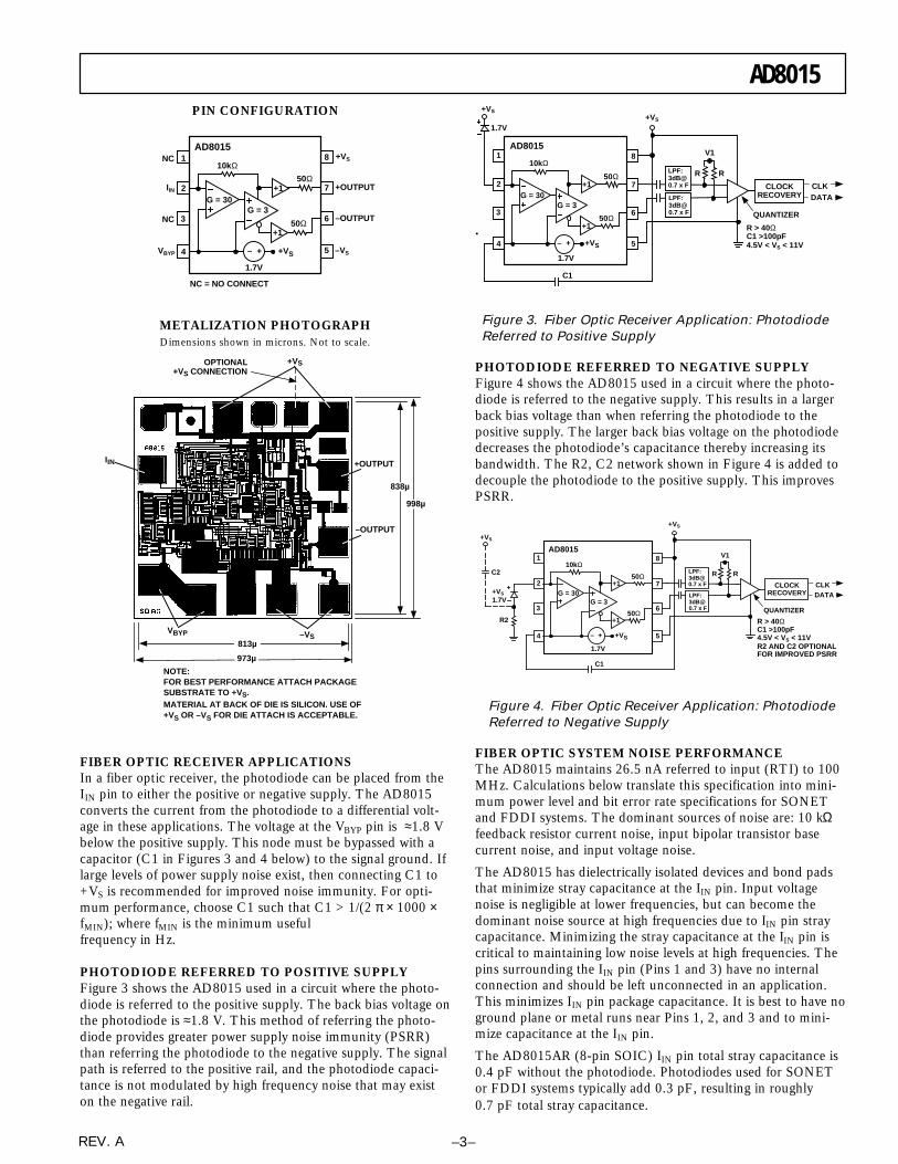
PIN CONFIGURATION
10kΩ
5
6
7
8
4
3
2
1AD8015
50Ω+1
NC
IIN
NC
VBYP –VS
–OUTPUT
+OUTPUT
+VS
G = 3G = 30
NC = NO CONNECT
50Ω+1
– + +VS
1.7V
METALIZATION PHOTOGRAPHDimensions shown in microns. Not to scale.
FIBER OPTIC RECEIVER APPLICATIONSIn a fiber optic receiver, the photodiode can be placed from theIIN pin to either the positive or negative supply. The AD8015converts the current from the photodiode to a differential volt-age in these applications. The voltage at the VBYP pin is ≈1.8 Vbelow the positive supply. This node must be bypassed with acapacitor (C1 in Figures 3 and 4 below) to the signal ground. Iflarge levels of power supply noise exist, then connecting C1 to+VS is recommended for improved noise immunity. For opti-mum performance, choose C1 such that C1 > 1/(2 π × 1000 ×fMIN); where fMIN is the minimum usefulfrequency in Hz.
PHOTODIODE REFERRED TO POSITIVE SUPPLYFigure 3 shows the AD8015 used in a circuit where the photo-diode is referred to the positive supply. The back bias voltage onthe photodiode is ≈1.8 V. This method of referring the photo-diode provides greater power supply noise immunity (PSRR)than referring the photodiode to the negative supply. The signalpath is referred to the positive rail, and the photodiode capaci-tance is not modulated by high frequency noise that may existon the negative rail.
OPTIONAL+VS CONNECTION
+OUTPUT
–OUTPUT
IIN
VBYP
973µ
998µ
+VS
838µ
–VS813µ
NOTE:FOR BEST PERFORMANCE ATTACH PACKAGESUBSTRATE TO +VS.MATERIAL AT BACK OF DIE IS SILICON. USE OF+VS OR –VS FOR DIE ATTACH IS ACCEPTABLE.
REV. A–4–
AD8015
SONET OC-3 SENSITIVITY ANALYSISOC-3 Minimum Bandwidth = 0.7 × 155 MHz ≈ 110 MHz
Total Current Noise = (π/2) × 26.5 nA
= 42 nA (assuming single pole response)
To maintain a BER < 1 × 10⁻¹⁰ (1 error per 10 billion bits):
Minimum current level needs to be > 13 × Total Current Noise= 541 nA (peak)
Assume a typical photodiode current/power conversion ratio = 0.85 A/W
Sensitivity (minimum power level) = 541/0.85 nW
= 637 nW (peak)
= –32.0 dBm (peak)
= –35.0 dBm (average)
The SONET OC-3 specification allows for a minimum powerlevel of –31 dBm peak, or –34 dBm average. Using the AD8015provides 1 dB margin.
FDDI SENSITIVITY ANALYSISFDDI Minimum Bandwidth = 0.7 × 125 MHz ≈ 88 MHz
Total Current Noise = (π / 2) ×88 MHz
100 MHz× 26.5 nA
= 39 nA (assuming single pole response)
To maintain a BER < 2.5 × 10⁻¹⁰ (1 error per 4 billion bits):
Minimum current level needs to be > 12.6 × Total Current Noise= 492 nA (peak)
Assume a typical photodiode current/power conversion ratio= 0.85 A/W
Sensitivity (minimum power level) = 492/0.85 nW
= 579 nW (peak)
= –32.4 dBm (peak)
= –35.4 dBm (average)
The FDDI specification allows for a minimum power level of–28 dBm peak, or –31 dBm average. Using the AD8015 pro-vides 4.4 dB margin.
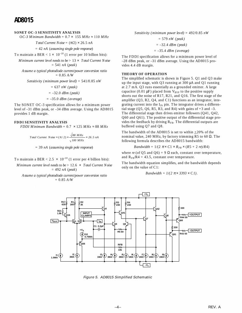
THEORY OF OPERATIONThe simplified schematic is shown in Figure 5. Q1 and Q3 makeup the input stage, with Q3 running at 300 µA and Q1 runningat 2.7 mA. Q3 runs essentially as a grounded emitter. A largecapacitor (0.01 µF) placed from VBYP to the positive supplyshorts out the noise of R17, R21, and Q16. The first stage of theamplifier (Q3, R2, Q4, and C1) functions as an integrator, inte-grating current into the IIN pin. The integrator drives a differen-tial stage (Q5, Q6, R5, R3, and R4) with gains of +3 and –3.The differential stage then drives emitter followers (Q41, Q42,Q60 and Q61). The positive output of the differential stage pro-vides the feedback by driving RFB. The differential outputs arebuffered using Q7 and Q8.
The bandwidth of the AD8015 is set to within +20% of thenominal value, 240 MHz, by factory trimming R5 to 60 Ω. Thefollowing formula describes the AD8015 bandwidth:
Bandwidth = 1/(2 π × C1 × RFB × (R5 + 2 re)/R4)
where re (of Q5 and Q6) = 9 Ω each, constant over temperature,and RFB/R4 = 43.5, constant over temperature.
The bandwidth equation simplifies, and the bandwidth dependsonly on the value of C1:
Bandwidth = 1/(2 π × 3393 × C1).
Q3
INPUTCLAMPS
Q1 IIN
Q16
R17635
R1300
R211.8k
VBYP
R23k
+VS
I100.75MA
C1 0.2pF
Q4
Q5
Q56
I11.5MA
I23MA
R5 60
R3230
Q41
RFB
Q6
R4230
Q7
+VS
Q42
Q8
330
330
–VS
+OUTPUTR44 50
R43 50
I31MA
I43MA
I53MA
I61MA
I71MA
I81MA
I91MA
10k
Q61
Q60
–OUTPUT
Figure 5. AD8015 Simplified Schematiic
AD8015
REV. A –5–
1.5
–1.5100
0
–1.0
–80
–0.5
–100
1.0
0.5
8040200 60–20–40–60
INPUT CURRENT – µA
OU
TP
UT
VO
LT
AG
E –
Vo
lts – 40°C
+ 25°C
+85°C
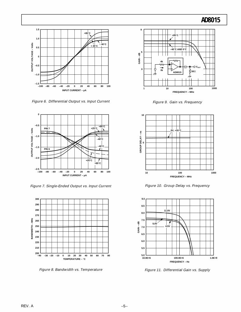
Figure 6. Differential Output vs. Input Current
0
–2.5100
–1.0
–2.0
–80
–1.5
–100
–0.5
806040200–20–40–60
INPUT CURRENT – µA
OU
TP
UT
VO
LT
AG
E –
Vo
lts PIN 7
PIN 6
+85°C+25°C
–40°C
+85°C+25°C
–40°C
Figure 7. Single-Ended Output vs. Input Current
300
20080
230
210
–30
220
–40
260
240
250
270
280
290
706050403020100–10–20
TEMPERATURE – °C
BA
ND
WID
TH
– M
Hz
Figure 8. Bandwidth vs. Temperature
9
1 10 100 1000
5
0
4k
AD8015
VOUT
IN
GA
IN –
dB
FREQUENCY – MHz
+85°C
–40°C AND 0°C
50Ω
Figure 9. Gain vs. Frequency
10
0
10 100 1000
5V, +25°C
FREQUENCY – MHz
GR
OU
P D
EL
AY
– n
s
Figure 10. Group Delay vs. Frequency
9.0
7.0
5.010.0E+6 100.0E+6 1.0E+9
6.5
6.0
5.5
7.5
8.0
8.5
FREQUENCY – Hz
GA
IN –
dB
11.0V
5.0V4.5V
Figure 11. Differential Gain vs. Supply
REV. A–6–
AD8015100
50
1 10 100 1000
FREQUENCY – MHz
0
5V, +25°C
PIN 7
PIN 6
IMP
ED
AN
CE
– Ω
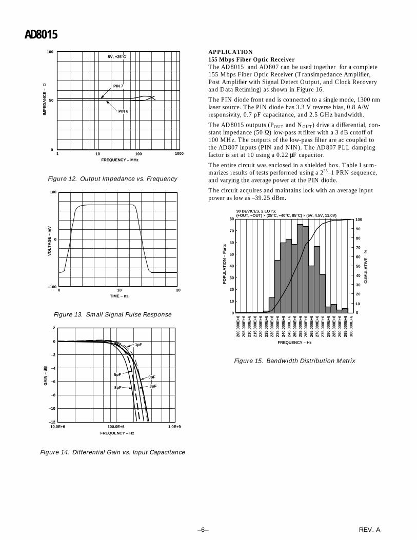
Figure 12. Output Impedance vs. Frequency
100
–100200
0
10
TIME – ns
VO
LT
AG
E –
mV
Figure 13. Small Signal Pulse Response
2
0
–1210.0E+6 100.0E+6 1.0E+9
–2
–4
–6
–8
–10
0pF
1pF
3pF
5pF
8pF
FREQUENCY – Hz
GA
IN –
dB
Figure 14. Differential Gain vs. Input Capacitance
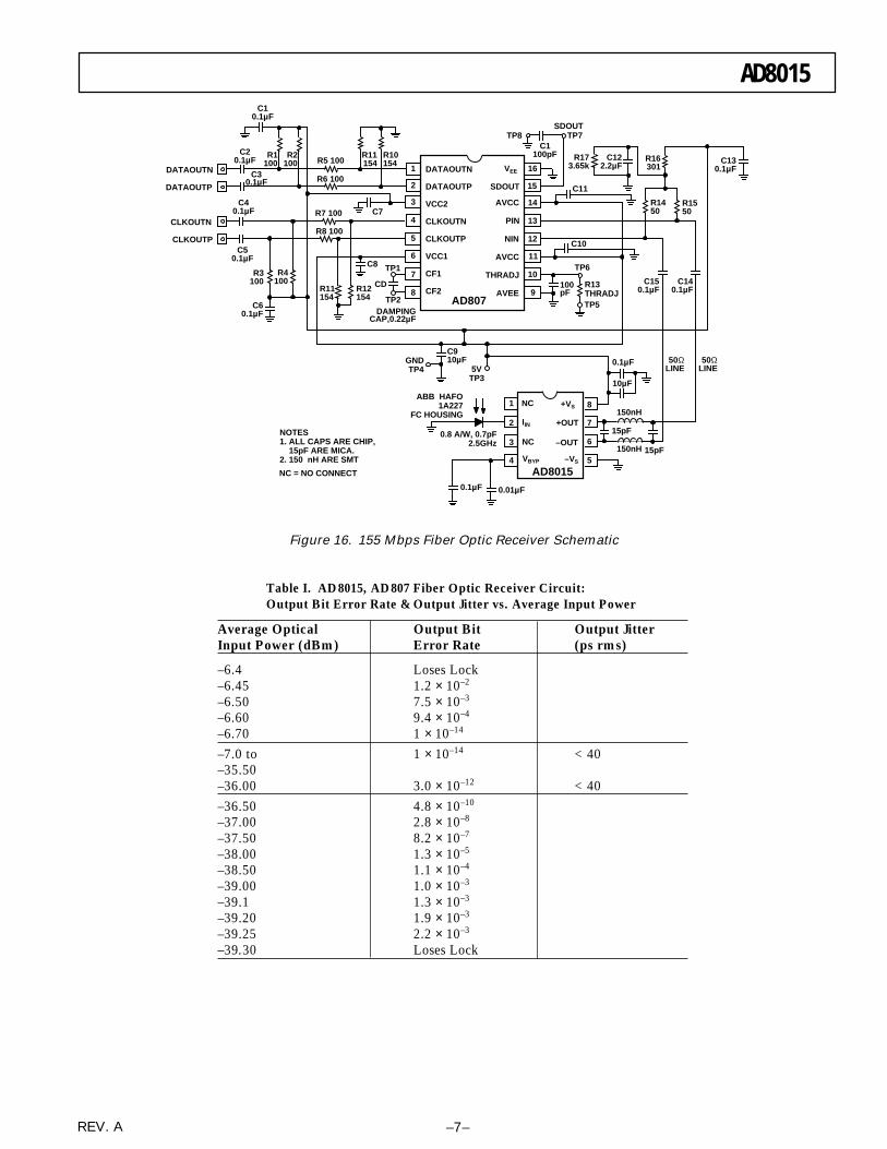
APPLICATION155 Mbps Fiber Optic ReceiverThe AD8015 and AD807 can be used together for a complete155 Mbps Fiber Optic Receiver (Transimpedance Amplifier,Post Amplifier with Signal Detect Output, and Clock Recoveryand Data Retiming) as shown in Figure 16.
The PIN diode front end is connected to a single mode, 1300 nmlaser source. The PIN diode has 3.3 V reverse bias, 0.8 A/Wresponsivity, 0.7 pF capacitance, and 2.5 GHz bandwidth.
The AD8015 outputs (POUT and NOUT) drive a differential, con-stant impedance (50 Ω) low-pass π filter with a 3 dB cutoff of100 MHz. The outputs of the low-pass filter are ac coupled tothe AD807 inputs (PIN and NIN). The AD807 PLL dampingfactor is set at 10 using a 0.22 µF capacitor.
The entire circuit was enclosed in a shielded box. Table I sum-marizes results of tests performed using a 223–1 PRN sequence,and varying the average power at the PIN diode.
The circuit acquires and maintains lock with an average inputpower as low as –39.25 dBm.
80
0
20
10
200.
000E
+6
40
30
50
60
70
80
0
20
10
40
30
50
60
70
90
100
205.
000E
+6
215.
000E
+622
0.00
0E+6
225.
000E
+623
0.00
0E+6
235.
000E
+624
0.00
0E+6
245.
000E
+625
0.00
0E+6
255.
000E
+626
0.00
0E+6
265.
000E
+627
0.00
0E+6
275.
000E
+628
0.00
0E+6
285.
000E
+629
0.00
0E+6
295.
000E
+630
0.00
0E+6
210.
000E
+6
30 DEVICES, 2 LOTS:(+OUT, –OUT) × (25°C, –40°C, 85°C) × (5V, 4.5V, 11.0V)
FREQUENCY – Hz
PO
PU
LA
TIO
N –
Par
ts
CU
MU
LA
TIV
E –
%Figure 15. Bandwidth Distribution Matrix
AD8015
REV. A –7–
NC = NO CONNECT
1
2
3
4
8
7
6
5
1
2
5
6
7
3
4
8
16
15
12
11
10
14
13
9
VEE
SDOUT
AVCC
PIN
NIN
AVCC
THRADJ
AVEEAD807
NC
IIN
NC
VBYP
+VS
+OUT
–VS
–OUT
R10154
R11154
R6 100
C7
R5 100R1
100R2
100
C10.1µF
C20.1µF
C30.1µF
DATAOUTN
DATAOUTP
CLKOUTN
CLKOUTP
C40.1µF
C60.1µF
R4100
R8 100
R7 100
R3100
C8
R12154
TP1
TP2DAMPING
CAP,0.22µF
R11154
C50.1µF
CD
TP8 TP7SDOUT
C1100pF
C11
TP6
TP5
100pF
R13THRADJ
C910µF
C10
GNDTP4
R1450
R1550
R16301
R173.65k
C130.1µF
5VTP3
AD8015
C150.1µF
15pF
10µF
0.1µF
15pF
0.1µF 0.01µF
ABB HAFO1A227
FC HOUSING
0.8 A/W, 0.7pF2.5GHz
NOTES1. ALL CAPS ARE CHIP, 15pF ARE MICA.2. 150 nH ARE SMT
C140.1µF
50ΩLINE
50ΩLINE
C122.2µF
150nH
150nH
DATAOUTN
DATAOUTP
VCC2
CLKOUTN
CLKOUTP
VCC1
CF1
CF2
Figure 16. 155 Mbps Fiber Optic Receiver Schematic
Table I. AD8015, AD807 Fiber Optic Receiver Circuit:Output Bit Error Rate & Output Jitter vs. Average Input Power
Average Optical Output Bit Output JitterInput Power (dBm) Error Rate (ps rms)
–6.4 Loses Lock–6.45 1.2 × 10⁻²
–6.50 7.5 × 10⁻³
–6.60 9.4 × 10⁻⁴
–6.70 1 × 10–14
–7.0 to 1 × 10–14 < 40–35.50–36.00 3.0 × 10⁻¹² < 40
–36.50 4.8 × 10⁻¹⁰
–37.00 2.8 × 10⁻⁸
–37.50 8.2 × 10⁻⁷
–38.00 1.3 × 10⁻⁵
–38.50 1.1 × 10⁻⁴
–39.00 1.0 × 10⁻³
–39.1 1.3 × 10⁻³
–39.20 1.9 × 10⁻³
–39.25 2.2 × 10⁻³
–39.30 Loses Lock
REV. A–8–
AD8015
PR
INT
ED
IN U
.S.A
.C
1973
–6–1
/96
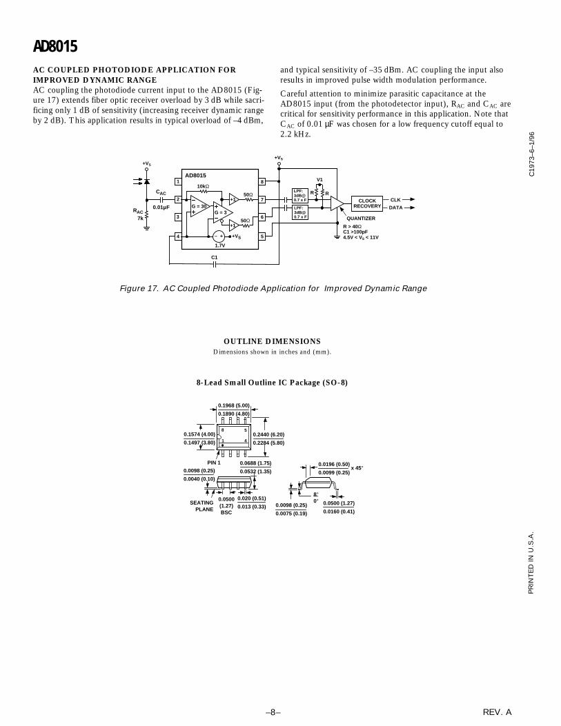
AC COUPLED PHOTODIODE APPLICATION FORIMPROVED DYNAMIC RANGEAC coupling the photodiode current input to the AD8015 (Fig-ure 17) extends fiber optic receiver overload by 3 dB while sacri-ficing only 1 dB of sensitivity (increasing receiver dynamic rangeby 2 dB). This application results in typical overload of –4 dBm,
and typical sensitivity of –35 dBm. AC coupling the input alsoresults in improved pulse width modulation performance.
Careful attention to minimize parasitic capacitance at theAD8015 input (from the photodetector input), RAC and CAC arecritical for sensitivity performance in this application. Note thatCAC of 0.01 µF was chosen for a low frequency cutoff equal to2.2 kHz.
OUTLINE DIMENSIONSDimensions shown in inches and (mm).
8-Lead Small Outline IC Package (SO-8)
0.1968 (5.00)
0.1890 (4.80)
8 5
41
PIN 1
0.1574 (4.00)
0.1497 (3.80)
0.0688 (1.75)
0.0532 (1.35)
SEATINGPLANE
0.0098 (0.25)
0.0040 (0.10)
0.020 (0.51)
0.013 (0.33)0.0500(1.27)BSC
0.0098 (0.25)
0.0075 (0.19)
0.0500 (1.27)
0.0160 (0.41)
8°0°
0.0196 (0.50)
0.0099 (0.25)x 45°
0.2440 (6.20)
0.2284 (5.80)
V1
+VS
CLOCKRECOVERYLPF:
LPF:[email protected] x F
QUANTIZER
R > 40ΩC1 >100pF4.5V < VS < 11V
CLK
DATA
RR
C1
10kΩ
5
6
7
8
4
3
2
1AD8015
50Ω+1
G = 3G = 30
50Ω+1
– + +VS
1.7V
+VS
CAC
0.01µFRAC7k
Figure 17. AC Coupled Photodiode Application for Improved Dynamic Range